


MSA-0311-TR1
Table of contents
 Loading...
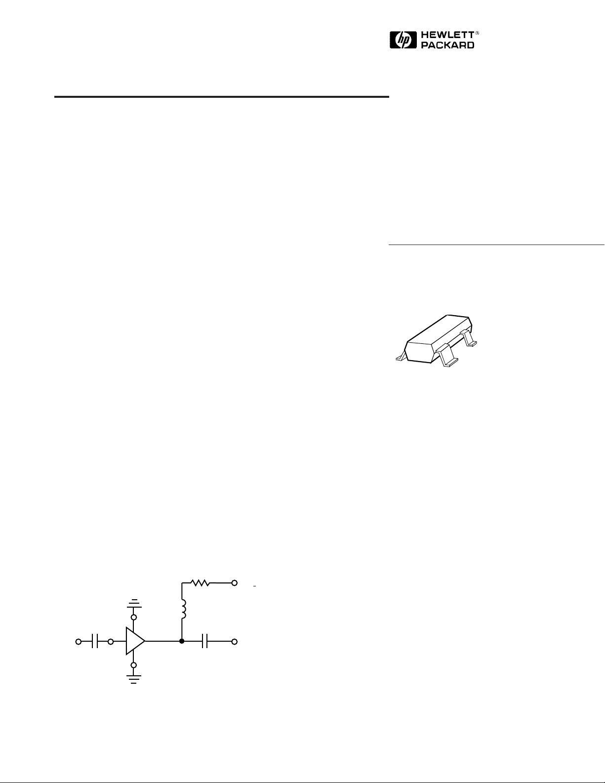
Cascadable Silicon Bipolar
MMIC␣ Amplifier
Technical Data
MSA-0311
Features
• Cascadable 50 Ω Gain Block
• 3 dB Bandwidth:
DC to 2.3 GHz
• 11.0 dB Typical Gain at
1.0␣ GHz
• 9.0 dBm Typical P
1 dB
at
--1.0␣ GHz
• Unconditionally Stable
(k>1)
• Low Cost Surface Mount
Plastic Package
• Tape-and-Reel Packaging
Option Available
Note:
1. Refer to PACKAGING section “Tapeand-Reel Packaging for Semiconductor Devices”.
[1]
The MSA-0311 is a low cost silicon
bipolar Monolithic Microwave
Integrated Circuit (MMIC) housed
in the surface mount plastic
SOT-143 package. This MMIC is
designed for use as a general
purpose 50 Ω gain block. Typical
applications include narrow and
broad band IF and RF amplifiers
in commercial and industrial
applications.
The MSA-series is fabricated using
HP’s 10 GHz fT, 25␣ GHz f
silicon bipolar MMIC process
which uses nitride self-alignment,
ion implantation, and gold metalli-
Typical Biasing Configuration
R
bias
SOT-143 PackageDescription
zation to achieve excellent
performance, uniformity and
,
MAX
V
> 7 V
CC
reliability. The use of an external
bias resistor for temperature and
current stability also allows bias
flexibility.
RFC (Optional)
C
block
IN OUT
MSA
V
= 4.7 V
d
C
block
5965-9567E
6-298
MSA-0311 Absolute Maximum Ratings
Parameter Absolute Maximum
Device Current 60 mA
Power Dissipation
[2,3]
240 mW
RF Input Power +13 dBm
Junction Temperature 150°C
Storage Temperature –65 to 150° C
[1]
Thermal Resistance
θjc = 500°C/W
Notes:
1. Permanent damage may occur if
any of these limits are exceeded.
2. T
3. Derate at 2.0 mW/° C for T
CASE
= 25°C.
4. See MEASUREMENTS section
“Thermal Resistance” for more
Electrical Specifications
[1]
, T
A
= 25° C
Symbol Parameters and Test Conditions: Id = 35 mA, Z
G
P
Power Gain (|S21|2) f = 0.1 GHz dB 11.5
= 50 Ω Units Min. Typ. Max.
O
information.
f = 1.0 GHz 9.0 11.0
∆G
f
3 dB
VSWR
Gain Flatness f = 0.1 to 1.6 GHz dB ±0.7
P
3 dB Bandwidth GHz 2.3
Input VSWR f = 0.1 to 3.0 GHz 1.5:1
Output VSWR f = 0.1 to 3.0 GHz 1.7:1
NF 50 Ω Noise Figure f = 1.0 GHz dB 6.0
P
IP
t
V
1 dB
3
D
d
Output Power at 1 dB Gain Compression f = 1.0 GHz dBm 9.0
Third Order Intercept Point f = 1.0 GHz dBm 22.0
Group Delay f = 1.0 GHz psec 140
Device Voltage T
= 25° C V 3.8 4.7 5.6
C
dV/dT Device Voltage Temperature Coefficient mV/°C –8.0
Notes:
1. The recommended operating current range for this device is 20 to 40 mA. Typical gain performance as a function of
current is on the following page.
[2,4]
> 30° C.
C
:
Part Number Ordering Information
Part Number No. of Devices Container
MSA-0311-TR1 3000 7" Reel
MSA-0311-BLK 100 Antistatic Bag
For more information, see “Tape and Reel Packaging for Semiconductor Devices”.
6-299
Loading...