


HITACHI
SERVICE MANUAL
HCPT
 No.014T-E
MODEL : C29-TF640S C29-TF650S
: " " ""
CAUTION: Before servicing this chassis, it is important that the service technician reads the "Safety Precaution" and " Product Safety Notices" in this Service Manual.
……………………… 4……………………… 4.……...………………………………… 6..………………………………… 6
...…………………………………………………… 7
.…………………………………… 8
…..…………………………………………… 9. …. ……………………………………… 10 - 16
...….…………. …………………… 16 - 21
...………………………………………… 21 - 26...…...…………………………………………… 21 - 38
CONTENTS
SAFETY PRECAUTIONS .…………………………………… 2 PRODUCT SAFETY NOTICE .….…………………………… 2 SPECIFICATIONS .…………………………………………… 6 REMOTE CONTROL UNIT…………………………………… 6 CONTROLS …………..……………………………………… 7 GENERAL OPERATIONS GUIDE ..………………………… 8 BLOCK DIAGRAM ……………………………………………9 CIRCUIT DESCRIPTION . …………………………………… 10 - 16 ADJUSTMENT INSTRUCTIONS ...………………………… 16 - 21 TROUBLESHOOTING .….…………………………………… 21 - 26 REPLACEMENT PARTS LIST ...…………………………… 27 - 38
SPECIFICATIONS AND PARTS ARE SUBJECT TO CHANGE FOR IMPROVEMENT.
COLOR TELEVISION
March 2004 Hitachi Consumer Products (Thailand) Ltd.

TECHNICAL CAUTIONS
SAFETY PRECAUTIONS
WARNING: Since the chassis of this |
receiver |
is connected |
|
to one |
side of the mains Supply during operation. service |
||
should |
not be attempted by anyone |
unfamiliar |
with the |
precautions necessary when working on this type of equipment. The following precautions should be opserved.
1.Do not install , remove, or handel the picture tube in any manner unless shatter-proof goggles are worn. People not so equipped should be kept away while picture tubes are handled. Keep picture tube away from the body while handing.
2.When replacing chassis in the cabinet. All the protective
devices are put back in place , such as ; barriers , nonmetallic knobs , adjustment and compartment cover or shields, isolation resistorscapacitors, etc.
3.When service is required, observe the original lead dress. Extra care should be taken to assure correct lead dress in the high voltage circuitry area.
4.Always use the manufacturer ' s replacement component. Especially critical components as indicated on the circuit diagram should not be replaced by other maker.
Furthermore where a short circuit has occurred, replace those components that indicate evidevce of overheating.
5.Before returning a serviced receiver to the customer, the service technician must thoroughtly test the unit to be
certain that it is completely safe to |
operate without danger |
||||||
of electrical |
shock, |
and |
be |
sure |
that no |
protetive device |
|
built into the instrucment by the manufacturer has became |
|||||||
defactive, |
or |
inadvertenly |
defeated during servicing. |
||||
therefore, the following checks are recommended for the |
|||||||
continued |
protection |
of |
the |
customers |
and service |
||
techninians. |
|
|
|
|
|
|
|
INSULATION
Insulation |
resistance |
between |
the main poles and |
a ny |
||
accessible |
metal parts |
should |
not be less than 7MΩ at 500V |
|||
CD. Also, |
no flashover |
or |
breakdown should occur |
during the |
||
dielectric |
strength |
test, |
to |
apply 4KV AC for one minute |
||
between the mains |
poles |
and |
any accessible metal |
parts. |
||
X-RADIATION
TUBES : The primary source of |
X radiation in |
this receiver |
|||||
is the picture tube. |
The |
tube |
utilized in |
this |
chassis is |
||
specially constructed |
to |
limit X radiation. |
|
|
|||
Fof continued |
X radiation |
protection, the replacement tube must |
|||||
be the same |
type as |
the |
original, |
HITACHI |
approved type. |
||
High |
Voltage |
|
|
|
|
This |
receiver is |
provided with a |
hold down |
circuit |
for |
clearly indicating |
that voltage has |
increased in |
excess |
of |
|
a predetermined value. Comply with all notes described in this Service Manual regarding this hold down circuit when servicing, so that this hold down circuit is operated correctly.
Serviceman Warning
With minimum Black Level and Picture. The operating high voltage in this receiver is lower than 33.0kV. In case any componant having influence on the high voltage is replaced. confirm that high voltage with minimum Brightness and contrast is lower than 35.0kV. To measure H.V. use a high impedance. H.V.meter. Connect (-) to chassis earth and (+) to the CRT anode button. (See the following connection diagram.
NOTE : Turn the power seitch off without fail before the connection to the Anode button is made
( + )
CRT ANODE
( - )
HIGH IMPEDANCE
H.V. METER
CHASSIS GROUND
PRODUCT SAFETY NOTICE
Many electrical and mechanical parts in HITACHI television receiver have special safety related characteristics. These characteristics are often not evident from visual inpection
nor can be protection afforded by them necessarily be obtained by using replacement components rated for higher voltage, wattage, etc. Replacement parts which have these special safety characteristecs are identified in this Service Manual. Electrical components having such features are identfied by marking with
a  mark in the schematics and on the replacement parts list in this Service Manual. The use of a substitute replacement component which does not have the same safety characteristics as the HITACHI recommended replacement one shown in the parts list in this Service Manual, may create electrical shock, fire, X radiation, or other hazards. Product Safety is continuously under review and new instructions are issued from time to time. For the
latest information, always consult the current HITACHI Service Manual. A subscription to, or additional copies of , HITACHI Service Manual may be obtained at a nominal charge from your HITACHI sales offices.
- 2 -
TECHNICAL CAUTIONS
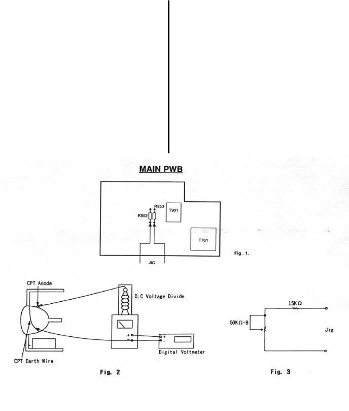
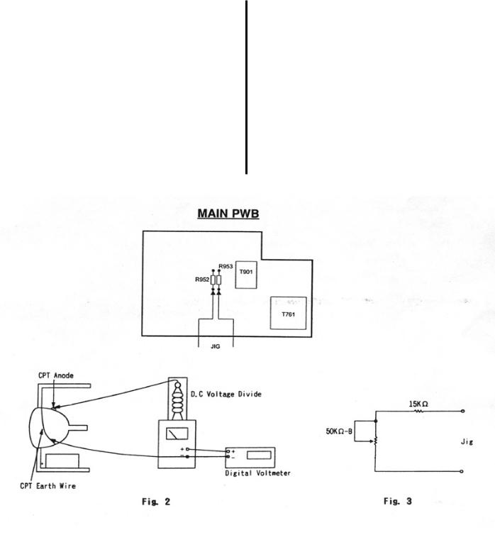
High voltage Iimiter circuit operation check
1.Connect the high voltage voltmeter between the CPT anode (anode cap) and GND (CPT grounding lead).
2.Receive the broadcast signal and set the brightness and contrast VRs to max. Set the beam current to 1.6mA + 10%.
(After cut-off adjustment)
3.Set the AC input voltage to 220 + 3V.
4.Check that the constant high voltage is 30.0 + 1.0kV at
this time.
5.Turn the switch of the set to off and connect the jig shown in Fig.3 at R952, R953 as shown in Fig 1.
6.With the brightness and contrast VRs left as set in item. 2 and with the AC input voltage stabilized at 220 V. turn the picture disapears with a high voltage of 34.0 or less.
7.Turn the switch of the set to off immediately after the check is completed.
8.Remove the adjust jigs and high voltmeter.
NOTE : When connecting disconnecting the high voltage voltmeter to from the anode cap, be sure to turn the switch of the set off and do it after the residual high voltage is discharged to the chassis because the high voltage may remain at the anode cap.
- 3 -
:220
1.,
2.Knob( )
3. มาตรฐานกําหนดทุกชิ้นสวน
|
|
|
|
- |
|||
|
|
|
|||||
|
|
|
|
|
|||
|
|
|
|
||||
5. ลําดับดังนี้
7 500Break Down4 kV DC 1
HOLD DOWN
33.0
Brightness Contrast35H.V. meter CRT anode ( )
: ANODE
( + )
 CRT ANODE ( - )
HIGH IMPEDANCE
H.V. METER
VOLTAGE
- 4 -
1. |
HIGH VOLTAGE VOLTMETER |
|
6. 2 (BRIGHTNESS + CONTRASS = MAX) 220 VAC |
|||||||||
|
ANODE CAP |
|
|
|
H.V. |
34.5 |
||||||
2. |
|
|
BRIGHTNESS |
|
|
|
|
|
|
|||
|
CONTRAST BEAM CURRENT 1.6 |
|
7. POWER SWITCH |
|||||||||
|
+ 10% |
|
|
|
|
|
|
|
|
|
||
3. |
220 + 3 |
|
8. ADJUST JIGS HIGH VOLTAGE VOLTMETER |
|||||||||
4. |
29.5 + 10% |
|
: |
HIGH VOLTAGE VOLTMETER |
||||||||
5. |
|
|
JIG 3 R952, R953 |
|
ANODE CAP POWER SWITHC |
|||||||
|
1 |
|
|
|
|
|
DISCHARGE |
|||||
|
|
|
|
|
|
|
|
|
|
|
||
1
|
|
3 |
|
2 |
|||
|
|
||
|
|
|
- 5 -
SPECIFICATION ( )
|
625-LINES |
B.G/D.K/H PAL |
|
|
B.G/D.K/K1 SECAM |
Recepstemtion system |
525-LINES |
NTSC50 |
M/NTSC |
||
|
|
NTSC3.58-5.5/6.0/6.5 |
|
|
NTSC4.43-5.5/6.0/6.5 |
|
|
PAL 60, SECAM 60 |
|
CCIR |
: E2~12, E21~69, S01~3, |
|
|
S1~41 |
|
Australia |
: AU0~12, AU28~69 |
Channel coverage |
OIRT |
: R1~12, R21~69 |
(Frequencey44MHz-863MHzrange ) |
JAPAN |
: J1~12, J13~69 |
|
U.S.A |
: US2~13, J~W, US14~69 |
|
Hong Kong, U.K. : UK21~69 |
|
|
China |
: C1~12, C13~57, Z1~38 |
* Soecifcations are subject to change wihout notice to improve performance.
Antenna input |
|
75W COAXIAL IEC TYPE |
||
|
||||
Color picture tube |
|
A68QCU770X56L |
|
|
Speaker (cm) |
|
6X12 (X2) |
|
|
Sound output |
|
7W X 2 |
|
: AC 240V 50Hz |
|
|
751 |
|
|
|
|
191A |
|
: AC 127V 50Hz/60Hz |
Power supply |
|
071, 98*, 192 |
} |
: AC 110V - 240V 50Hz/60Hz |
|
|
121, 195 |
||
|
|
|
||
|
|
941, 08*, 051 |
} |
: AC 200V - 240V 50Hz/60Hz |
|
|
433 , 435 |
||
|
|
|
||
Power consumption |
|
138 W |
|
|
Weight (kg) |
|
45.5 KG |
|
|
Dimensions |
|
768 X 593 X 503 (C29-TF640S) |
||
W x H x D (mm) |
|
769 X 593 X 491 (C29-TF650S) |
||
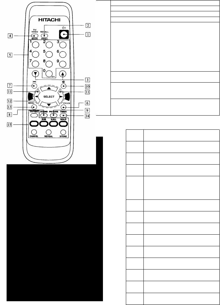
REMOTE CONTROL UNIT ( )
1
2
3
4
5
6
7
8
9
10
11
12
13
14
15
POWER ON/OFFSEITCH
/
RECALL
PROGRAMME UP/DOWN
/
INPUT SELECTION
PROGRAMME SELECTOR
CH I/CH II
2
SURROUND
SOUND (Sub - - for T/TEXT)
( Sub - -) PICTUR (U.N.L. - - for T/TEXT)
( U.N.L. - -) MUTE
VOLUME UP/DOWN
/
CURSOR
MENU
Timer (Hold - - for T/TEXT)
( Hold - -) TELETEXT OPERATING KEYS (081/982only)
( 081/982 )
- 6 -
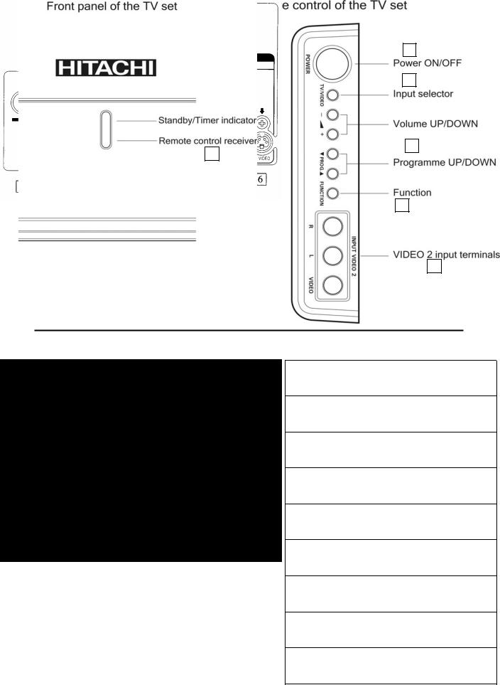
CONTROL ( )
1
7
2 |
|
|
|
8 |
|
|
|
|
9
5
4
6
Rear Panel ( )
1 |
POWER NO/OFF SWITCH |
|
||||
/ |
|
|
|
|||
2 |
STANDBY/TIMER INDICATION |
|||||
|
/ |
|||||
3 |
AERIAL TERMINAL |
|
|
|||
|
|
|
|
|||
4 |
FUNCTION |
|
|
|
||
|
|
|||||
5 |
REMOTE CONTROL RECEIVER |
|||||
|
||||||
6 |
AV IN/OUT TERMINAL |
|
||||
|
AV / |
|
||||
7 |
INPUT SELECT |
|
|
|
||
|
|
|
||||
8 |
VOLUME UP/DOWN |
|
|
|||
/ |
|
|
||||
9 |
PROGRAMME UP/DOWN |
|
||||
|
/ |
|
|
|||
- 7 -
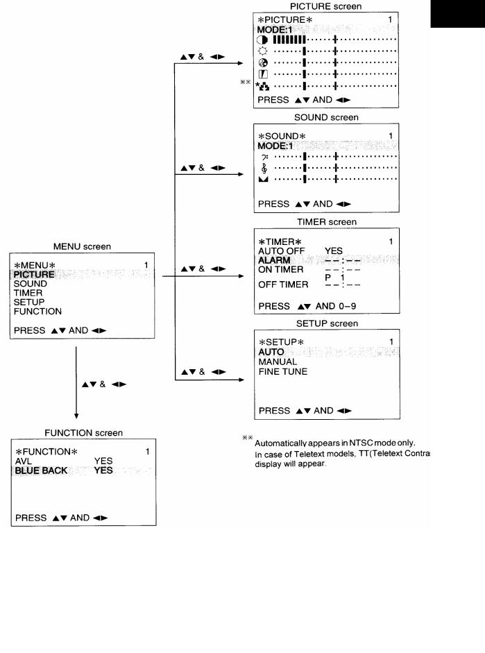
GENERAL ORERATIONS GUIDE ( )
With this TV set, all adjustments/settings are performed by |
selecting from |
menu screens. |
|
|
|||||
Different menu screens and details |
of adjustments/settings |
are shown below. To access the menu |
screen, press |
||||||
the |
|
|
|
button, then select the |
item by pressing the up/down cursor |
buttons and setting it by |
pressing the left/ |
||
|
MENU |
|
|||||||
right |
cursor |
buttons. |
|
|
|
|
|
||
|
|
|
|
|
|
|
|
|
|
|
|
|
|
|
|
|
|
|
|
- 8 -

3
- 9 -

CIRCUIT DESCRIPTION ( )
Selection and CPU circuitry
IC type, TDA9384/86/65, performs functions like IIC controls, channel selection, on-screen displays, search tuning, systems selection amongst others. The pin's functions of TDA9384/86/65 are oresebted in the table shown bellow.
IC |
TDA9384/86/65 |
IIC IC |
, |
||||||
, , , |
|
IC |
|
||||||
TDA9384/86/65 |
|
|
|
|
|
|
|||
|
|
|
|
|
|
|
|
|
|
Pin |
Signal |
|
I/O |
Configuration |
|
|
Function |
|
|
number |
name |
|
|
|
|
|
|||
|
|
|
|
|
|
|
|
||
1 |
Power |
|
Output |
P.P |
3.3V |
O = Stand - by, 1 = on |
|
|
|
2 |
SCL |
|
I/O |
O.D |
5V |
Colck of main I2 C-bus |
|
|
|
3 |
SDA |
|
I/O |
O.D |
5V |
Data of main I2 C-bus |
|
|
|
4 |
Alarm |
|
Output |
O.D |
5V |
PWM output for Beep sound |
|
|
|
5 |
SAW Sw |
|
Output |
O.D |
3.3V |
1 = M, 0 = Others |
|
|
|
6 |
AV S-DET |
|
Input |
H.I. |
5V |
Detect for S-VHS (not mono chassis) |
|
|
|
|
SW FE/AV |
|
Output |
O.D |
5V |
FE/AV switch (mono chassis) |
|
|
|
7 |
Key-In |
|
Input |
H.I. |
3.3V |
Local analogue keyboard |
|
|
|
8 |
V2 / V1 |
|
Output |
O.D |
3.3V |
1=Video:2, 0=Video:1 |
|
|
|
9 |
VSSC / P |
|
- |
- |
|
Digital ground for u-controller core and periphery |
|
|
|
10 |
Led |
|
Output |
O.D |
3.3V |
LED Drive |
|
|
|
11 |
ON/OFF Mute |
|
Output |
O.D |
3.3V |
1=Mute on, 0=Mute off (Under Standby) |
|
|
|
12 |
VSSA |
|
- |
- |
|
Analog ground of Teletext decoder and digital ground |
|
||
|
|
|
|
|
|
of TV-processor |
|
|
|
13 |
SECPLL |
|
- |
- |
|
SECAM PLL decoupling |
|
|
|
14 |
VP2 |
|
- |
- |
|
2nd supply voltage TV-processor (+8V ) |
|
|
|
15 |
DECDIG |
|
- |
- |
|
Decoupling digital supply of TV-processor |
|
|
|
16 |
PH2LF |
|
- |
- |
|
Phase2-filter |
|
|
|
17 |
PH1LF |
|
- |
- |
|
Phase1-filter |
|
|
|
18 |
TV |
|
- |
- |
|
Ground 3 of TV-processor |
|
|
|
19 |
DECBG |
|
- |
- |
|
Bandgap decoupling |
|
|
|
20 |
AVL / EWD |
|
Output |
- |
|
East-West drive output |
|
|
|
21 |
VDRB |
|
Output |
- |
|
Vertical drive B output |
|
|
|
22 |
VDRA |
|
Output |
- |
|
Vertical drive A output |
|
|
|
23 |
IFIN 1 |
|
Input |
- |
|
IF input 1 |
|
|
|
24 |
IFIN 2 |
|
Input |
- |
|
IF input 2 |
|
|
|
25 |
IREF |
|
Input |
- |
|
Reference current input |
|
|
|
26 |
VSC |
|
- |
- |
|
Vertical sawtooth capacitor |
|
|
|
27 |
AGCOUT |
|
Output |
- |
|
Tuner AGC output |
|
|
|
28 |
AUDEEM |
|
Output |
- |
|
Audio deemphasis |
|
|
|
29 |
DECSDEM |
|
- |
- |
|
Decoupling sound demodulator |
|
|
|
- 10 -
Pin |
Signal |
|
I/O |
|
|
Configuration |
|
Function |
number |
name |
|
|
|
|
|||
|
|
|
|
|
|
|
||
30 |
GND2 |
|
- |
|
|
- |
|
Gound 2 for TV processor |
31 |
SNDPLL |
|
- |
|
|
- |
|
Narrow band PLL filter |
32 |
REFO |
|
Output |
|
|
- |
|
Subcarrier reference output |
33 |
HOUT |
|
Output |
|
|
- |
|
Horizontal output |
34 |
FBISO |
|
Input |
|
|
- |
|
Flyback input |
35 |
AUDEXT |
|
Input |
|
|
- |
|
External audio input |
36 |
EHTO |
|
Input |
|
|
- |
|
EHT/overvoltage protection input |
37 |
PLLIF |
|
- |
|
|
- |
|
IF-PLL loop filter |
38 |
IFOut |
|
Output |
|
|
- |
|
IF-video output / selected CVBS output |
39 |
+8v |
|
- |
|
|
- |
|
Main supply voltage TV-processor ( +8V ) |
40 |
CVBSINT |
|
Input |
|
|
- |
|
Internal CVBS input |
41 |
GND1 |
|
- |
|
|
- |
|
Ground 1 for TV-processor |
42 |
CVBS/Yin |
|
Input |
|
|
- |
|
External CVBS input |
43 |
Cin |
|
Input |
|
|
- |
|
Chrominance input ( SVHS ) |
44 |
AUDOUT |
|
Output |
|
|
- |
|
Audio output |
45 |
INSSW2 |
|
- |
|
|
- |
|
No connection |
46 |
R2/VIN |
|
- |
|
|
- |
|
No connection |
47 |
G2/YIN |
|
- |
|
|
- |
|
No connection |
48 |
B2/UIN |
|
- |
|
|
- |
|
No connection |
49 |
BCLIN |
|
Input |
|
|
- |
|
Beam current limiter input/V-guard input |
50 |
BLKIN |
|
Input |
|
|
- |
|
Black current input |
51 |
RO |
|
Output |
|
|
- |
|
Red OSD output |
52 |
GO |
|
Output |
|
|
- |
|
Green OSD output |
53 |
BO |
|
Output |
|
|
- |
|
Blue OSD output |
54 |
VDDA |
|
- |
|
|
- |
|
Analog supply of Teletext decoder and digital supply |
|
|
|
|
|
|
|
|
of TV-processor (3.3V) |
55 |
VPE |
|
- |
|
|
- |
|
OTP Programming Voltage |
56 |
VDDC |
|
- |
|
|
- |
|
Digital supply to core (3.3V) |
57 |
OSDGND |
|
- |
|
|
- |
|
Oscillator ground supply |
58 |
XTA/IN |
|
Input |
|
|
- |
|
Crystal oscillator input |
59 |
XTA/OUT |
|
Output |
|
|
- |
|
Crystal oscillator output |
60 |
RESET |
|
Input |
|
|
- |
|
Reset |
61 |
VDDP |
|
- |
|
|
- |
|
Digital supply to periphery (+3.3 V) |
62 |
SCL(EEP) |
|
I/O |
|
|
O.D |
3.3V |
Clock of secondary I2-bus for EEPROM |
63 |
SDA(EEP) |
|
I/O |
|
|
O.D |
3.3V |
Data of secondary I2-bus for EEPROM |
64 |
RC-In |
|
Input |
|
|
O.D |
3.3V |
Input for Remote control decoding |
Note 1: |
Abbreviation of configuration mode: |
|
|
O.D. |
Open Drain |
|||
|
( comfiguration mode:) |
|
Q.B. |
Quasi-Bidirectional |
||||
|
|
|
|
|
|
|
H.I. |
High-Impedance |
|
|
|
|
|
|
|
P.P |
Push-Pull |
Note 2: |
During reset all pins are in Quasi-Bidirectional mode. |
|
|
|||||
|
( |
|
Quasi Bidirectional) |
|
||||
- 11 -
POWER SUPPLY CIRCUIT
1. Stand-dy mode :
Commutating voltage from AC input is rectified by D931~D934 and produces approximately 300V. This high voltage DC is applied to the primary winding of T931 in series with the integrated high voltage MOSFET inside the I931 (TNY254). The diode D935, capacitor C936, and resistor R930 comprise the clamp circuit that limits the turn-off voltage spike on the drain pin 5 of I931 to a safe value. The secondary winding of T931 is rectified and filtered by D971, C971, L971, and C973 to provide the 5V output. Additional filtering are provided by L972 and C972. The output voltage is determined dy the sum of the opto-coupling I932 forward drop (about 1V) and zener diode D972 voltage.
1. :
D931~D934 300VT931 MOSFET I931(TNY254) D935 , C936 , R930 turn-off voltage spike drain 5 I931T931 D971 , C971 , L971 , C9735 V opto-coupling I932 ( 1 V)D972
2. Turn-on mode :
When TV set turn-on, the on/off signal from MICON become high, so RL901 turns on, commutating voltage from AC input is rectified by D901A and produces approximately 300V to pin 3 of I901. Current flowing through R903, R904, R918, R919 causes I901 pin 4 to initially turn on. Secondary voltage are then induced winding B1-B2 in T901, I901 supply voltage is obtained via R910, D906, C909, C909A and applied to pin 4 of I901, thereby maintaining I902 switching operation. Secondary voltage in S1 - S4 winding is rectified by D952 to produce 24V which is smoothed by C956.
Error amplifier Q951 is set to a pre-determined level by resistor network R950~R953, and reference voltage D953. Should the +B voltage rise, base voltage of transistor Q951 will become more positive, and this difference is amplified by the error amplified by Q951. An output is applied to I901 feedback pin 1 through opto-coupling I902 and controls ON time of I901 internal circuit. In this way, +B voltage is regulated and maintained at a constant level. D959 and D957 offer protection that it should the voltage level rise excessively When standby mode is selected, RL901 turn off. Only+5V still live
2. :
/ MICON HIGH RL901D901A 300V 3 I901 R903 , R904 , R918 , R919 4 I901
B1-B2 T901 R910 , D906 , C909 , C909A 4I901 I902 Switching S1-S2 D961+B 130V C956 S2-S4 D952 24VC956
- 12 -
 Loading...