


®
43
Power Quality Analyzer
Service Manual
4822 872 05377
September 1998, Rev. 3, 07/00
© 1998, 2000 Fluke Corporation, All rights reserved. Printed in the Netherlands All product names are trademarks of their respective companies.
SERVICE CENTERS
To locate an authorized service center, visit us on the World Wide Web:
http://www.fluke.com
or call Fluke using any of the phone numbers listed below: +1-888-993-5853 in U.S.A. and Canada +31-402-678-200 in Europe
+1-425-356-5500 from other countries
Table of Contents
Chapter |
|
Title |
Page |
1 |
Safety Instructions............................................................................. |
1-1 |
|
|
1.1 |
Introduction............................................................................................. |
1-3 |
|
1.2 |
Safety Precautions ................................................................................... |
1-3 |
|
1.3 |
Caution and Warning Statements............................................................. |
1-3 |
|
1.4 |
Symbols .................................................................................................. |
1-3 |
|
1.5 |
Impaired Safety ....................................................................................... |
1-4 |
|
1.6 |
General Safety Information...................................................................... |
1-4 |
2 |
Characteristics................................................................................... |
2-1 |
|
|
2.1 |
Introduction............................................................................................. |
2-3 |
|
2.2 |
Safety Specifications ............................................................................... |
2-3 |
|
2.3 |
Function Specifications ........................................................................... |
2-4 |
|
2.3.1 Electrical functions........................................................................... |
2-4 |
|
|
2.3.2 Scope ............................................................................................... |
2-5 |
|
|
2.3.3 Meter................................................................................................ |
2-7 |
|
|
2.3.4 Record.............................................................................................. |
2-7 |
|
|
2.4 |
Miscellaneous.......................................................................................... |
2-8 |
|
2.5 |
Current Probe .......................................................................................... |
2-8 |
|
2.6 |
Environmental Conditions ....................................................................... |
2-9 |
|
2.7 |
Electromagnetic Immunity....................................................................... |
2-10 |
3 |
Circuit Descriptions........................................................................... |
3-1 |
|
|
3.1 |
Introduction............................................................................................. |
3-3 |
|
3.2 |
Block Diagram ........................................................................................ |
3-3 |
|
3.2.1 Input 1 - Input 2 Measurement Circuits ............................................ |
3-3 |
|
|
3.2.2 Trigger Circuit.................................................................................. |
3-5 |
|
|
3.2.3 Digital Circuit .................................................................................. |
3-5 |
|
|
3.2.4 Power Circuit ................................................................................... |
3-6 |
|
|
3.2.5 Start-up Sequence, Operating Modes ................................................ |
3-7 |
|
|
3.3 |
Detailed Circuit Descriptions................................................................... |
3-9 |
|
3.3.1 Power Circuit ................................................................................... |
3-9 |
|
|
3.3.2 Input 1 - Input 2 Measurement Circuits ............................................ |
3-14 |
|
|
3.3.3 Trigger Circuit.................................................................................. |
3-20 |
|
i

43
Service Manual
|
3.3.4 Digital Circuit .................................................................................. |
3-24 |
|
4 |
Performance Verification .................................................................. |
4-1 |
|
|
4.1 |
Introduction............................................................................................. |
4-3 |
|
4.2 |
Equipment Required For Verification ...................................................... |
4-3 |
|
4.3 |
How To Verify ........................................................................................ |
4-3 |
|
4.4 |
Display and Backlight Test...................................................................... |
4-4 |
|
4.5 |
Input 1 and Input 2 Tests in the SCOPE MODE. ..................................... |
4-5 |
|
4.5.1 Input 1 Trigger Sensitivity Test ........................................................ |
4-6 |
|
|
4.5.2 Input 1 Frequency Response Upper Transition Point Test................. |
4-7 |
|
|
4.5.3 Input 1 Frequency Measurement Accuracy Test................................ |
4-7 |
|
|
4.5.4 Input 2 Frequency Measurement Accuracy Test................................ |
4-9 |
|
|
4.5.5 Input 2 Trigger Level and Trigger Slope Test ................................... |
4-10 |
|
|
4.5.6 Input 2 Trigger sensitivity Test......................................................... |
4-12 |
|
|
4.5.7 Input 1 Trigger Level and Trigger Slope Test ................................... |
4-13 |
|
|
4.5.8 Input 1 and 2 DC Voltage Accuracy Test.......................................... |
4-15 |
|
|
4.5.9 Input 1 and 2 AC Voltage Accuracy Test.......................................... |
4-17 |
|
|
4.5.10 Input 1 and 2 AC Input Coupling Test ............................................ |
4-19 |
|
|
4.5.11 Input 1 and 2 Volts Peak Measurements Test.................................. |
4-20 |
|
|
4.5.12 Input 1 and 2 Phase Measurements Test.......................................... |
4-21 |
|
|
4.5.13 Input 1 and 2 High Voltage AC & DC Accuracy Test..................... |
4-22 |
|
|
4.6 |
Ohms/Continuity/Capacitance. ................................................................ |
4-25 |
|
4.6.1 Resistance Measurements Test. ........................................................ |
4-25 |
|
|
4.6.2 Diode Test Function Test ................................................................. |
4-26 |
|
|
4.6.3 Continuity Function Test.................................................................. |
4-26 |
|
|
4.6.4 Capacitance Measurements Test ....................................................... |
4-27 |
|
|
4.7 |
Inrush Current. ........................................................................................ |
4-28 |
|
4.8 |
Sags & Swells ......................................................................................... |
4-29 |
|
4.9 |
Harmonics............................................................................................... |
4-30 |
|
4.10 VOLT/AMPS/HERTZ........................................................................... |
4-30 |
|
|
4.11 POWER. ............................................................................................... |
4-31 |
|
|
4.12 Transients.............................................................................................. |
4-32 |
|
5 |
Calibration Adjustment...................................................................... |
5-1 |
|
|
5.1 |
General.................................................................................................... |
5-3 |
|
5.1.1 Introduction...................................................................................... |
5-3 |
|
|
5.1.2 Calibration number and date............................................................. |
5-3 |
|
|
5.1.3 General Instructions.......................................................................... |
5-4 |
|
|
5.2 |
Equipment Required For Calibration ....................................................... |
5-4 |
|
5.3 |
Starting Calibration Adjustment .............................................................. |
5-4 |
|
5.4 |
Contrast Calibration Adjustment.............................................................. |
5-6 |
|
5.5 |
Warming Up & Pre-Calibration ............................................................... |
5-7 |
|
5.6 |
Final Calibration...................................................................................... |
5-7 |
|
5.6.1 HF Gain Input 1. .............................................................................. |
5-8 |
|
|
5.6.2 Delta T Gain, Trigger Delay Time & Pulse Adjust Input 1 ............... |
5-9 |
|
|
5.6.3 Gain DMM (Gain Volt).................................................................... |
5-10 |
|
|
5.6.4 Volt Zero.......................................................................................... |
5-12 |
|
|
5.6.5 Gain Ohm......................................................................................... |
5-12 |
|
|
5.6.6 Capacitance Gain Low and High ...................................................... |
5-13 |
|
|
5.6.7 Capacitance Clamp & Zero............................................................... |
5-14 |
|
|
5.6.8 Capacitance Gain.............................................................................. |
5-14 |
|
|
5.7 |
Save Calibration Data and Exit................................................................ |
5-15 |
6 |
Disassembling ................................................................................... |
6-1 |
|
ii
|
|
|
Contents (continued) |
|
6.1. Introduction............................................................................................ |
6-3 |
|
|
6.2. Disassembling Procedures ...................................................................... |
6-3 |
|
|
6.1.1 Required Tools................................................................................. |
6-3 |
|
|
6.2.2 Removing the Battery Pack .............................................................. |
6-3 |
|
|
6.2.3 Removing the Bail............................................................................ |
6-3 |
|
|
6.2.4 Opening the Test Tool...................................................................... |
6-3 |
|
|
6.2.5 Removing the Main PCA Unit.......................................................... |
6-5 |
|
|
6.2.6 Removing the Display Assembly...................................................... |
6-6 |
|
|
6.2.7 Removing the Keypad and Keypad Foil............................................ |
6-6 |
|
|
6.3 |
Disassembling the Main PCA Unit .......................................................... |
6-6 |
|
6.4 |
Reassembling the Main PCA Unit ........................................................... |
6-8 |
|
6.5 |
Reassembling the Test Tool..................................................................... |
6-8 |
7 |
Corrective Maintenance .................................................................... |
7-1 |
|
|
7.1 |
Introduction............................................................................................. |
7-3 |
|
7.2 |
Starting Fault Finding.............................................................................. |
7-4 |
|
7.3 |
Charger Circuit........................................................................................ |
7-4 |
|
7.4 |
Starting with a Dead Test Tool ................................................................ |
7-6 |
|
7.4.1 Test Tool Completely Dead.............................................................. |
7-6 |
|
|
7.4.2 Test Tool Software Does not Run..................................................... |
7-7 |
|
|
7.4.3 Software Runs, Test Tool not Operative ........................................... |
7-7 |
|
|
7.5 |
Miscellaneous Functions ......................................................................... |
7-7 |
|
7.5.1 Display and Back Light .................................................................... |
7-7 |
|
|
7.5.2 Fly Back Converter .......................................................................... |
7-8 |
|
|
7.5.3 Slow ADC........................................................................................ |
7-9 |
|
|
7.5.4 Keyboard.......................................................................................... |
7-10 |
|
|
7.5.5 Optical Port (Serial RS232 Interface)................................................ |
7-11 |
|
|
7.5.6 Input Channel 1 and 2 Voltage Measurements .................................. |
7-11 |
|
|
7.5.7 Ohms and Capacitance Measurements .............................................. |
7-12 |
|
|
7.5.8 Trigger Functions ............................................................................. |
7-13 |
|
|
7.5.9 Reference Voltages........................................................................... |
7-14 |
|
|
7.5.10 Buzzer Circuit ................................................................................ |
7-14 |
|
|
7.5.11 Reset ROM Line (ROMRST) ......................................................... |
7-14 |
|
|
7.5.12 RAM Test ...................................................................................... |
7-14 |
|
|
7.5.13 Power ON/OFF .............................................................................. |
7-15 |
|
|
7.5.14 PWM Circuit.................................................................................. |
7-15 |
|
|
7.5.15 Randomize Circuit.......................................................................... |
7-15 |
|
8 |
List of Replaceable Parts .................................................................. |
8-1 |
|
|
8.1 |
Introduction............................................................................................. |
8-3 |
|
8.2 |
How to Obtain Parts ................................................................................ |
8-3 |
|
8.3 |
Final Assembly Parts............................................................................... |
8-4 |
|
8.4 |
Main PCA Unit Parts............................................................................... |
8-6 |
|
8.5 |
Main PCA Parts ...................................................................................... |
8-7 |
|
8.6 |
Accessory Replacement Parts .................................................................. |
8-23 |
9 |
Circuit Diagrams ................................................................................ |
9-1 |
|
|
9.1 |
Introduction............................................................................................. |
9-3 |
|
9.2 |
Schematic Diagrams................................................................................ |
9-3 |
10 |
Modifications...................................................................................... |
10-1 |
|
|
10.1 Software modifications.......................................................................... |
10-3 |
|
|
10.2 Hardware modifications......................................................................... |
10-3 |
|
iii
List of Tables
Table |
Title |
Page |
1-1. |
Symbols ............................................................................................................ |
1-3 |
2-1. |
No Visible Disturbance...................................................................................... |
2-10 |
2-2. |
Disturbance < 1 % ............................................................................................. |
2-10 |
2-3. |
Disturbance < 10 % ........................................................................................... |
2-10 |
3-1. |
Fluke 43 Main Blocks ....................................................................................... |
3-3 |
3-2. |
Fluke 43 Operating Modes ................................................................................ |
3-8 |
3-3. |
Input 1 Voltage Ranges And Trace Sensitivity................................................... |
3-17 |
3-4. |
Ohms Ranges, Trace Sensitivity, and Current .................................................... |
3-18 |
3-5. |
Capacitance Ranges, Current, and Pulse Width.................................................. |
3-19 |
3-6. |
D-ASIC PWM Signals ...................................................................................... |
3-27 |
4-1. |
Input 1 Frequency Measurement Accuracy Test................................................. |
4-8 |
4-2. |
Volts DC Measurement Verification Points ....................................................... |
4-17 |
4-3. |
Volts AC Measurement Verification Points ....................................................... |
4-19 |
4-4. |
Input 1 and 2 AC Input Coupling Verification Points ........................................ |
4-20 |
4-5. |
Volts Peak Measurement Verification Points ..................................................... |
4-21 |
4-6. |
Phase Measurement Verification Points............................................................. |
4-22 |
4-7. |
V DC and V AC High Voltage Verification Tests.............................................. |
4-25 |
4-8. |
Resistance Measurement Verification Points...................................................... |
4-26 |
4-9. |
Capacitance Measurement Verification Points ................................................... |
4-27 |
4-10. |
Volts/AMPS/HERZ verification points.............................................................. |
4-31 |
4-11. |
Power Measurement Verification points ............................................................ |
4-31 |
5-1. |
HF Gain Calibration Points Fast ........................................................................ |
5-9 |
5-2. |
HF Gain Calibration Points Slow....................................................................... |
5-9 |
5-3. |
Volt Gain Calibration Points <300V.................................................................. |
5-11 |
5-4. |
Ohm Gain Calibration Points............................................................................. |
5-13 |
7-1. |
Starting Fault Finding........................................................................................ |
7-4 |
8-1. |
Final Assembly Parts......................................................................................... |
8-4 |
8-2. |
Main PCA Unit ................................................................................................. |
8-6 |
8-3. |
Main PCA ......................................................................................................... |
8-7 |
9-1. |
Parts Location Main PCA Side 1 ....................................................................... |
9-4 |
9-2. |
Parts Location Main PCA Side 2 ....................................................................... |
9-5 |
v
List of Figures
Figure |
Title |
Page |
2-1. |
Max. Input Voltage vs. Frequency ..................................................................... |
2-4 |
3-1. |
Fluke 43 Block Diagram.................................................................................... |
3-2 |
3-2. |
Fluke 43 Start-up Sequence, Operating Modes................................................... |
3-8 |
3-3. |
Power Supply Block Diagram............................................................................ |
3-9 |
3-4. |
CHAGATE Control Voltage.............................................................................. |
3-11 |
3-5. |
Fly-Back Converter Current and Control Voltage .............................................. |
3-12 |
3-6. |
Fly-Back Converter Block Diagram................................................................... |
3-13 |
3-7. |
Back Light Converter Voltages.......................................................................... |
3-14 |
3-8. |
C-ASIC Block Diagram..................................................................................... |
3-15 |
3-9. |
Capacitance Measurement ................................................................................. |
3-19 |
3-10. |
T-ASIC Trigger Section Block Diagram............................................................ |
3-20 |
3-11. Random Repetitive Sampling Mode .................................................................. |
3-22 |
|
3-12. |
Reference Voltage Section................................................................................. |
3-23 |
3-13. |
LCD Control ..................................................................................................... |
3-26 |
4-1. |
Display Pixel Test Pattern ................................................................................. |
4-4 |
4-2. |
Test Tool Input 1 to 5500A Scope Output 50Ω.................................................. |
4-6 |
4-3. |
Test Tool Input 2 to 5500A NORMAL output ................................................... |
4-9 |
4-4. |
Test Tool Input 1 to 5500A Normal Output ....................................................... |
4-13 |
4-5. |
Test Tool Input 1-2 to 5500A Normal Output .................................................... |
4-15 |
4-6. |
Test Tool Input 1-2 to 5500A Normal Output for >300V................................... |
4-22 |
4-7. |
Test Tool Input 1 to 5500A Normal Output 4-Wire ........................................... |
4-25 |
4-8. |
Test Tool Input 2 to 5500A NORMAL output ................................................... |
4-28 |
4-9. |
Test Tool Input 1 & 2 5500A Normal Output .................................................... |
4-29 |
4-10. |
Bargraph Harmonics Volt.................................................................................. |
4-30 |
4-11. |
Bargraph Harmonics Ampere............................................................................. |
4-30 |
4-12. |
Test Tool Input 1 to 5500A Normal Output ....................................................... |
4-32 |
5-1. |
Version & Calibration Screen ............................................................................ |
5-3 |
5-2. |
Display Test Pattern .......................................................................................... |
5-7 |
5-3. |
HF Gain Calibration Input Connections............................................................. |
5-8 |
5-4. |
5500A Scope Output to Input 1 ......................................................................... |
5-10 |
5-5. |
Volt Gain Calibration Input Connections <300V ............................................... |
5-11 |
5-6. |
Volt Gain Calibration Input Connections 500V ................................................. |
5-12 |
5-7. |
Four-wire Ohms calibration connections............................................................ |
5-13 |
5-8. |
Capacitance Gain Calibration Input Connections ............................................... |
5-14 |
6-1. |
Fluke 43 Main Assembly................................................................................... |
6-4 |
vii

43
Service Manual
6-2. |
Flex Cable Connectors....................................................................................... |
6-5 |
6-3. |
Main PCA Unit Assembly................................................................................. |
6-7 |
6-4. |
Mounting the display shielding bracket.............................................................. |
6-9 |
6-5. |
Battery pack installation .................................................................................... |
6-9 |
7-1. |
Operative Test Tool without Case...................................................................... |
7-3 |
8-1. |
Fluke 43 Final Assembly................................................................................... |
8-5 |
8-2. |
Main PCA Unit ................................................................................................. |
8-7 |
9-1. |
Circuit Diagram 1, Channel 1 Circuit ................................................................ |
9-7 |
9-2. |
Circuit Diagram 2, Channel 2 Circuit ................................................................ |
9-8 |
9-3. |
Circuit Diagram 3, Trigger Circuit..................................................................... |
9-9 |
9-4. |
Circuit Diagram 4, Digital Circuit ..................................................................... |
9-10 |
9-5. |
Circuit Diagram 4 (cont), Digital Circuit Keyboard ........................................... |
9-11 |
9-6. |
Circuit Diagram 5, Power Circuit ...................................................................... |
9-12 |
9-7. |
Main PCA side 1, PCB Version <3.................................................................... |
9-13 |
9-8. |
Main PCA side 2, PCB Version <3.................................................................... |
9-14 |
9-9. |
Main PCA side 1, PCB version 3....................................................................... |
9-15 |
9-10. |
Main PCA side 2, PCB version 3....................................................................... |
9-16 |
viii
Chapter 1
Safety Instructions
|
Title |
Page |
1.1 |
Introduction............................................................................................. |
1-3 |
1.2 |
Safety Precautions ................................................................................... |
1-3 |
1.3 |
Caution and Warning Statements............................................................. |
1-3 |
1.4 |
Symbols .................................................................................................. |
1-3 |
1.5 |
Impaired Safety ....................................................................................... |
1-4 |
1.6 |
General Safety Information...................................................................... |
1-4 |
1-1
Safety Instructions 1
1.1 Introduction
1.1 Introduction
Read these pages carefully before beginning to install and use the instrument.
The following paragraphs contain information, cautions and warnings which must be followed to ensure safe operation and to keep the instrument in a safe condition.
Warning
Servicing described in this manual is to be done only by qualified service personnel. To avoid electrical shock, do not service the instrument unless you are qualified to do so.
1.2 Safety Precautions
For the correct and safe use of this instrument it is essential that both operating and service personnel follow generally accepted safety procedures in addition to the safety precautions specified in this manual. Specific warning and caution statements, where they apply, will be found throughout the manual. Where necessary, the warning and caution statements and/or symbols are marked on the instrument.
1.3 Caution and Warning Statements
Caution
Used to indicate correct operating or maintenance procedures to prevent damage to or destruction of the equipment or other property.
Warning
Calls attention to a potential danger that requires correct procedures or practices to prevent personal injury.
1.4 Symbols
Table 1-1 shows the symbols used on the test tool or in this manual.
Table 1-1. Symbols
Read the safety information in the Users Manual
Equal potential inputs, connected internally
DOUBLE INSULATION (Protection
Class)
Static sensitive components (black/yellow).
Live voltage |
Recycling information |
Earth |
Disposal information |
Conformité Européenne |
|
1-3

43
Service Manual
1.5 Impaired Safety
Whenever it is likely that safety has been impaired, the instrument must be turned off and disconnected from line power. The matter should then be referred to qualified technicians. Safety is likely to be impaired if, for example, the instrument fails to perform the intended measurements or shows visible damage.
1.6 General Safety Information
Warning
Removing the instrument covers or removing parts, except those to which access can be gained by hand, is likely to expose live parts and accessible terminals which can be dangerous to life.
The instrument shall be disconnected from all voltage sources before it is opened.
Capacitors inside the instrument can hold their charge even if the instrument has been separated from all voltage sources.
Components which are important for the safety of the instrument may only be replaced by components obtained through your local FLUKE organization. These parts are indicated with an asterisk (*) in the List of Replaceable Parts, Chapter 8.
1-4
Chapter 2
Characteristics
|
Title |
Page |
2.1 |
Introduction............................................................................................. |
2-3 |
2.2 |
Safety Specifications ............................................................................... |
2-3 |
2.3 |
Function Specifications ........................................................................... |
2-4 |
2.3.1 Electrical functions........................................................................... |
2-4 |
|
2.3.2 Scope ............................................................................................... |
2-5 |
|
2.3.3 Meter................................................................................................ |
2-7 |
|
2.3.4 Record.............................................................................................. |
2-7 |
|
2.4 |
Miscellaneous.......................................................................................... |
2-8 |
2.5 |
Current Probe .......................................................................................... |
2-8 |
2.6 |
Environmental Conditions ....................................................................... |
2-9 |
2.7 |
Electromagnetic Immunity....................................................................... |
2-10 |
2-1

Characteristics 2
2.1 Introduction
2.1 Introduction
Safety Characteristics
The Fluke 43 has been designed and tested in accordance with Standards ANSI/ISA S82.01-1994, EN 61010.1 (1993) (IEC 1010-1), CAN/CSA-C22.2 No.1010.1-92 (including approval), UL3111-1 (including approval) Safety Requirements for Electrical Equipment for Measurement, Control, and Laboratory Use.
This manual contains information and warnings that must be followed by the user to ensure safe operation and to keep the instrument in a safe condition. Use of this equipment in a manner not specified by the manufacturer may impair protection provided by the equipment.
Performance Characteristics
FLUKE guarantees the properties expressed in numerical values with the stated tolerance. Specified non-tolerance numerical values indicate those that could be nominally expected from the mean of a range of identical ScopeMeter test tools.
Environmental Data
The environmental data mentioned in this manual are based on the results of the manufacturer’s verification procedures.
2.2 Safety Specifications
Safety Characteristics
Designed and tested for measurements on 600 Vrms Category III, Pollution Degree 2 in accordance with:
•EN 61010.1 (1993) (IEC 1010-1)
•ANSI/ISA S82.01-1994
•CAN/CSA-C22.2 No.1010.1-92 (including approval)
•UL3111-1 (including approval)
Installation Category III refers to distribution level and fixed installation circuits inside a building.
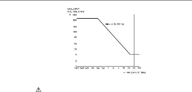
Maximum input voltage Input 1 and 2 |
|
|
Direct on inputs or with test leads TL24............................................. |
(see Figure 2-1) |
|
0 to 66 kHz .............................................................................................. |
600 |
Vrms |
> 66 kHz.................................................................................... |
derating to 5 |
Vrms |
With Shielded Banana-to-BNC Adapter Plug BB120 ......................... |
(see Figure 2-1) |
|
0 to 400 kHz ............................................................................................ |
300 |
Vrms |
> 400 kHz.................................................................................. |
derating to 5 |
Vrms |
2-3
43
Service Manual
|
|
|
|
|
|
|
|
|
|
|
|
|
|
|
|
|
|
|
|
|
|
|
|
|
|
|
|
ST8571 |
|
|
|
|
|
|
|
|
|
|
|
|
|
|
|
|
|
|
|
|
|
|
|
|
|
|
|
|
|
|
|
|
|
|
|
|
|
|
|
|
|
|
|
|
|
|
|
|
|
|
|
|
|
|
|
|
|
|
|
|
|
|
|
|
|
|
|
|
|
|
|
|
|
|
|
|
|
|
|
|
|
|
|
|
|
|
|
|
|
|
|
|
|
|
|
|
|
|
|
|
|
|
|
|
|
|
|
|
|
|
|
|
|
|
|
|
|
|
|
|
|
|
|
|
|
|
|
|
|
|
|
|
|
|
|
|
|
|
|
|
|
|
|
|
|
|
|
|
|
|
|
|
|
|
|
|
|
|
|
|
|
|
|
|
|
|
|
|
|
|
|
|
|
|
|
|
|
|
|
|
|
|
|
|
|
|
|
|
|
|
|
|
|
|
|
|
|
|
|
|
|
|
|
|
|
|
|
|
|
|
|
|
|
|
|
|
|
|
|
|
|
|
|
|
|
|
|
|
|
|
|
|
|
|
|
|
|
|
|
|
|
|
|
|
|
|
|
|
|
|
|
|
|
|
|
|
|
|
|
|
|
|
|
|
|
|
|
|
|
|
|
|
|
|
|
|
|
|
|
|
|
|
|
|
|
|
|
|
|
|
|
|
|
|
|
|
|
|
|
|
|
|
|
|
|
|
|
|
|
|
|
|
|
|
|
|
|
|
|
|
|
|
|
|
|
|
|
|
|
|
|
|
|
|
|
|
|
|
|
|
|
|
|
|
|
|
|
|
|
|
|
|
|
|
|
|
|
|
|
|
|
|
|
|
|
|
|
|
|
|
|
|
|
|
|
|
|
Figure 2-1. Max. Input Voltage vs. Frequency |
|
|||||||||||||||||||||||||||
Maximum floating voltage |
|
|||||||||||||||||||||||||||
From any terminal to ground |
|
|||||||||||||||||||||||||||
0 to 400 Hz ............................................................................................. |
600 Vrms |
|||||||||||||||||||||||||||
2.3 Function Specifications
The accuracy of all measurements is within ± (% of reading + number of counts) from 18 °C to 28 °C. For all specifications, probe specifications must be added.
2.3.1 Electrical functions
Specifications are valid for signals with a fundamental between 40 and 70 Hz.
Minimum input voltage ............................................................................. |
4 V peak-peak |
Minimum input current............................................................ |
10 A peak-peak (1 mV/A) |
Input bandwidth.............................................. |
DC to 15 kHz (unless specified otherwise) |
Volts / Amps / Hertz |
|
Readings ................................................................... |
Vrms (ac+dc), Arms (ac+dc), Hz |
Voltage ranges (auto) ..................................................... |
5 V; 50 V; 500 V; 1250 V |
minimum step........................................................... |
1 mV; 10 mV; 100 mV; 1 V |
|
±(1 % + 10 counts) |
Current ranges (auto)............................................... |
50.00 A to 500.0 kA, 1250 kA |
minimum step.................................................... |
10 mA; 0.1 A; 1 A; 100 A, 1 kA |
|
±(1 % + 10 counts) |
Frequency range...................................................................... |
10.0 Hz to 15.0 kHz |
40.0 to 70.0 Hz ...................................................................... |
±(0.5 % + 2 counts) |
resolution................................................................. |
0.1 Hz; 1 Hz; 10 Hz; 100 Hz |
Power |
|
Readings ....................................................................... |
Watt, VA, VAR, PF, DPF, Hz |
Watt, VA, VAR ranges (auto) .................... |
250 W to 250 MW, 625 MW, 1.56 GW |
when selected: total ( %r): ...................................................... |
±(2 % + 6 counts) |
when selected: fundamental ( %f):.......................................... |
±(4 % + 4 counts) |
DPF ..................................................................................................... |
0.00 to 1.00 |
0.00 to 0.25.................................................................................... |
not specified |
0.25 to 0.90.............................................................................................. |
± 0.04 |
0.90 to 1.00.............................................................................................. |
± 0.03 |
2-4
|
|
|
Characteristics |
2 |
|
|
|
2.3 Function Specifications |
|
PF........................................................................................................ |
|
|
0.00 to 1.00 |
|
|
|
|
± 0.04 |
|
Frequency range....................................................................... |
|
10.0 Hz to 15.0 kHz |
|
|
40.0 to 70.0 Hz ................................................................... |
|
±(0.5 % + 2 counts) |
|
|
Harmonics |
|
|
|
|
Number of harmonics ............................................................ |
|
DC..21, DC..33, DC..51 |
|
|
Readings / Cursor readings |
31st ±(5 % + 3 counts) |
51st ±(15 % + 5 counts) |
|
|
Vrms... |
fund. ±(3 % + 2 counts).... |
|
||
Irms .... |
fund. ±(3 % + 2 counts).... |
31st ±(5 % + 3 counts) ... |
51st ±(15 % + 5 counts) |
|
Watt.... |
fund. ±(5 % + 10 counts) .. |
31st ±(10 % + 10 counts)51st ±(30 % + 5 counts) |
|
|
Frequency of fundamental....................................................................... |
|
± 0.25 Hz |
|
|
Phase .................................................................................... |
|
|
fund. ±3° ... 51st ± 15° |
|
K-factor (in Amp and Watt) ......................................................................... |
|
± 10 % |
|
|
Sags & Swells |
|
|
|
|
Recording times (selectable) ............................. |
4 minutes to 8 days, endless (16 days) |
|
||
Readings / Cursor Readings |
|
|
|
|
Vrms actual, Arms actual (cycle by cycle calculation)............... |
±(2 % + 10 counts) |
|
||
Vrms max, Arms max (idem at cursor)...................................... |
±(2 % + 12 counts) |
|
||
Vrms average, Arms average (only at cursor) ............................ |
±(2 % + 10 counts) |
|
||
Vrms min, Arms min (idem at cursor)....................................... |
±(2 % + 12 counts) |
|
||
Transients |
|
|
|
|
Detection of voltage transients ......................................................................... |
|
> 40 ns |
|
|
Useful input bandwidth input 1 (with test leads TL24)............................ |
DC to 1 MHz |
|
||
Reference signal............................................................................................ |
|
Vrms, Hz |
|
|
After START, the Vrms and frequency of the signal are measured. |
|
|||
From these data a pure sine wave is calculated. |
|
|
||
Detection when transients exceed specified voltage level (selectable) |
|
|||
Voltage levels .................................. |
20 %, 50 %, 100 %, 200 % of reference signal |
|
||
Number of transient memories (temporary).............................................................. |
40 |
|
||
Cursor reading |
|
|
|
|
Vpeak min, Vpeak max at cursor ............................................... |
|
± 5 % of full scale |
|
|
Inrush |
|
|
|
|
Graphic display |
|
|
|
|
Current ranges (selectable) ................. |
1 A, 5 A, 10 A, 50 A, 100 A, 500 A, 1000 A |
|
||
Inrush times (selectable)......................................... |
1 s, 5 s, 10 s, 50 s, 100 s, 5 min |
|
||
Cursor readings |
|
|
|
|
A peak max at cursor 1 ............................................................... |
|
± 5 % of full scale |
|
|
A peak max at cursor 2 ............................................................... |
|
± 5 % of full scale |
|
|
Time between cursors ............................................................... |
|
±(0.2 % + 2 pixels) |
|
|
2.3.2 Scope |
|
|
|
|
Input Impedance |
|
1 MΩ // 12 pF (± 2 pF) |
|
|
Input 1 ..................................................................................... |
|
|
|
|
Input 2 ..................................................................................... |
|
|
1 MΩ // 10 pF (± 2 pF) |
|
Horizontal |
|
|
|
|
Time base modes (selectable)....................................................... |
|
Normal, Single, Roll |
|
|
Ranges (selectable within modes) |
|
|
|
|
In Normal ....................................................................................... |
|
5 s to 20 ns/div |
|
|
In Single shot.................................................................................... |
|
5 s to 1 µs/div |
|
|
In Roll mode..................................................................................... |
|
60 s to 1 s/div |
|
|
Time base error............................................................................ |
|
< ±(0.4 % + 1 pixel) |
|
|
2-5

43
Service Manual
Maximum sampling rate |
|
|
10 ms to 60 s................................................................................................ |
|
5 MS/s |
20 ns to 10 ms............................................................................................ |
|
25 MS/s |
Trigger source (auto)........................................................................ |
|
Input 1 or Input 2 |
Trigger |
|
|
Mode .................................................................................................... |
|
auto triggering |
Sources ...................................... |
Input 1, Input 2, Automatic (not manually selectable) |
|
Error for frequencies < 1 MHz |
|
± 0.5 div |
Voltage Level............................................................................................ |
|
|
at positive slope the top of the trigger symbol and at negative trigger the bottom of |
||
the trigger symbol is the trigger point. |
± 1 sample |
|
Time Delay Real Time sampling ............................................................ |
||
Time Delay Quasi Random sampling. ......................................................... |
± 10 ns |
|
Sensitivity input 1 |
|
≥ 4 div |
@ 40 MHz ................................................................................................... |
|
|
@ 25 MHz ................................................................................................ |
|
≥ 1.5 div |
@ DC - 5 MHz............................................................................ |
|
≥ 0.5 div or 5 mV |
Sensitivity input 2 |
|
≥ 0.5 div |
@ DC – 20 kHz ........................................................................................ |
|
|
Slope Selection ................................................................................ |
|
Positive, negative |
Level Control |
|
> ± 4 div, within dynamic range |
Range Manual control ........................................... |
|
|
Delay ( horizontal move )......... |
-10 div - 0 div, used for horizontal move functionality |
|
Vertical |
|
|
Voltage ranges ..................................................................... |
|
50.0 mV/div to 500 V/div |
Trace accuracy ............................................................................. |
|
±(1 % + 2 pixels) |
Bandwidth input 1 (voltage) |
|
|
excluding test leads or probes.............................................. |
DC to 20 MHz (-3 dB) |
|
with test leads TL24.............................................................. |
|
DC to 1 MHz (-3 dB) |
with 10:1 probe PM8918 (optional)..................................... |
DC to 20 MHz (-3 dB) |
|
with shielded test leads STL120 (optional)........................ |
DC to 12.5 MHz (-3 dB) |
|
|
|
DC to 20 MHz (-6 dB) |
Lower transition point (ac coupling).................................................. |
10 Hz (-3 dB) |
|
Bandwidth input 2 (current) |
|
|
with Banana-to-BNC adapter............................................................. |
DC to 15 kHz |
|
Lower transition point (ac coupling).................................................. |
10 Hz (-3 dB) |
|
Scope readings
The accuracy of all scope readings is valid from 18 °C to 28 °C with relative humidity up to 90 % for a period of one year after calibration. Add 0.1 x (the specified accuracy) for each °C below 18 °C or above 28 °C. More than one waveform period must be visible on the screen.
V dc, A dc..................................................................................... |
±(0.5 % + 5 counts) |
V ac and V ac+dc (True RMS) input 1 |
|
DC to 60 Hz.............................................................................. |
±(1 % + 10 counts) |
60 Hz to 20 kHz..................................................................... |
±(2.5 % + 15 counts) |
20 kHz to 1 MHz ...................................................................... |
±(5 % + 20 counts) |
1 MHz to 5 MHz..................................................................... |
±(10 % + 25 counts) |
5 MHz to 20 MHz................................................................... |
±(30 % + 25 counts) |
A ac and A ac+dc (True RMS) input 2 |
|
DC to 60 Hz.............................................................................. |
±(1 % + 10 counts) |
60 Hz to 15 kHz...................................................................... |
±(30 % + 25 counts) |
2-6
|
Characteristics |
2 |
|
2.3 Function Specifications |
|
Frequency (Hz), Pulse width, Duty cycle (2.0 % to 98.0 %) |
|
|
1 Hz to 1 MHz ......................................................................... |
±(0.5 % + 2 counts) |
|
1 MHz to 10 MHz....................................................................... |
±(1 % + 2 counts) |
|
10 MHz to 30 MHz.................................................................. |
±(2.5 % + 2 counts) |
|
Phase (Input 1 to Input 2) |
±2° |
|
Up to 60 Hz ...................................................................................................... |
|
|
60 Hz to 400 Hz................................................................................................ |
±5° |
|
Peak voltage |
|
|
Peak max, Peak min.................................................................... |
± 5 % of full scale |
|
Peak-peak ................................................................................. |
± 10 % of full scale |
|
Crest |
|
|
Range .................................................................................................... |
1.0 to 10.0 |
|
|
±(5 % + 1 count) |
|
2.3.3 Meter |
|
|
Ohm |
500.0 Ω to 5.000 MΩ, 30.00 MΩ |
|
Ranges..................................................................... |
|
|
|
±(0.6 % + 5 counts) |
|
Max. Measurement Current.............................................................................. |
0.5 mA |
|
Measurement Voltage at open circuit .................................................................. |
< 4 V |
|
Diode |
|
|
Accuracy........................................................................................... |
±(2 % +5 counts) |
|
Max. Measurement Current.............................................................................. |
0.5 mA |
|
Measurement Voltage at open circuit .................................................................. |
< 4 V |
|
Continuity |
< 30 Ω (± 5 Ω) |
|
Beep .................................................................................................... |
|
|
Measurement Current....................................................................................... |
0.5 mA |
|
Detection of shorts............................................................................................ |
> 1 ms |
|
Capacitance |
50.00 nF to 500.0 µF |
|
Ranges........................................................................................ |
|
|
|
±(2 % +10 counts) |
|
Max. Measurement Current.............................................................................. |
0.5 mA |
|
Temperature |
|
|
Ranges (°C or °F) ..................................... |
-100.0 to +400.0 °C or -200.0 to +800.0 °F |
|
|
±(0.5 % + 5 counts) |
|
2.3.4 Record |
|
|
Record times (selectable)............................................. |
4 min to 8 days, endless (16 days) |
|
Number of readings ......................................................................... |
1 or 2 simultaneously |
|
Record is available for the functions:
•volts / amps / hertz
•power
•harmonics
•ohms / continuity / capacitance
•temperature
•scope
2-7

43
Service Manual
2.4 Miscellaneous
Display |
|
|
Useful screen area ............................................................ |
|
72 x 72 mm (2.83 x 2.83 in) |
Resolution.......................................................................................... |
|
240 x 240 pixels |
Backlight ............................................................... |
|
Cold Cathode Fluorescent (CCFL) |
Power |
|
|
External |
|
|
Power Adapter .......................................................................................... |
|
PM8907 |
Input Voltage ..................................................................................... |
|
10 to 21 V dc |
Power.................................................................................................... |
|
5 W typical |
Internal |
|
|
Rechargeable Ni-Cd battery pack ................................................................. |
BP120 |
|
Voltage range........................................................................................ |
|
4 to 6 V dc |
Operating Time ........................................................................................... |
|
4 hours |
Charging Time ................................................................ |
|
4 hours with Fluke 43 off |
|
|
12 hours with Fluke 43 on |
Refresh cycle...................................................................................... |
|
8 to 14 hours |
Memory |
|
|
Number of screen memories..................................................................................... |
|
10 |
Number of transient memories (temporary) .............................................................. |
40 |
|
Mechanical |
|
|
Height x width x depth........................................ |
|
232 x 115 x 50 mm (9.1 x 4.5 x 2 in) |
Weight (including battery pack) ............................................................ |
|
1.1 kg (2.5 lb.) |
Interface ................................................................................... |
|
RS232, optically isolated |
Supported Printers........................ |
HP Deskjet®, Laserjet®, PostScript and Epson FX80 |
|
Serial via PM9080 (optically isolated RS232 Adapter/Cable). |
||
Parallel via PAC91 (optically isolated Print Adapter Cable, optional). |
||
To PC ....................................................................... |
|
Dump and load settings and data |
Serial via PM9080 (optically isolated RS232 adapter/cable), using SW43W (FlukeView® Power Quality Analyzer software).
2.5 Current Probe
 Safety Characteristics
Designed for measurements on 600 Vrms Category III. Protection class II, double or reinforced insulation requirements in accordance with:
•IEC 1010-1
•ANSI/ISA S82
•CSA-C22.2 No.1010.1-92
•UL1244
Electrical Specifications |
|
|
Current range ..................................................................................... |
1 A to 500 |
Arms |
AC current over range limit.......................................................................... |
700 |
Arms |
Maximum 10 minutes, followed by removal from current carrying conductor |
|
|
for 30 minutes. |
|
|
Output Signal......................................................................................... |
1 mV ac/A ac |
|
2-8
|
Characteristics |
2 |
|
2.6 Environmental Conditions |
|
Accuracy |
|
|
5 to 10 Hz |
|
|
1 to 500 A........................................................................................ |
-3 dB typically |
|
10 to 20 Hz |
± 5 % |
|
1 to 300 A...................................................................................................... |
|
|
300 to 400 A................................................................................................ |
± 15 % |
|
400 to 500 A................................................................................................ |
± 25 % |
|
20 to 45 Hz |
± 5 % |
|
1 to 500 A...................................................................................................... |
|
|
45 to 65 Hz |
±5 % of reading + 0.3 A |
|
1 to 20 A........................................................................... |
|
|
20 to 100 A.................................................................................... |
±5 % of reading |
|
|
± 3 ° phase shift |
|
100 to 500 A.................................................................................. |
±2 % of reading |
|
65 Hz to 3 kHz |
± 5 ° phase shift |
|
±(5 % + 0.4 A) |
|
|
1 to 50 A......................................................................................... |
|
|
50 to 500 A.................................................................................................... |
± 5 % |
|
Influence of temperature on accuracy .................................. |
<0.15 % per 10 °C (18 °F) |
|
Altitude |
|
|
During operation............................................................................. |
2.0 km (6560 feet) |
|
While stored ................................................................................. |
12 km (40 000 feet) |
|
2.6 Environmental Conditions |
|
|
Environmental ................................................... |
MIL 28800E, Type 3, Class III, Style B |
|
Temperature |
0 to 50 °C (32 to 122 °F) |
|
During operation................................................................... |
|
|
While stored ....................................................................... |
-20 to 60 °C (-4 to 140 °F) |
|
Humidity |
|
|
During operation: |
|
|
0 to 10 °C (32 to 50 °F) ............................................................... |
non-condensing |
|
10 to 30 °C (50 to 86 °F)...................................................................... |
95 % ± 5 % |
|
30 to 40 °C (86 to 104 °F)..................................................................... |
75 % ± 5 % |
|
40 to 50 °C (104 to 122 °F)................................................................... |
45 % ± 5 % |
|
While stored: |
|
|
-20 to 60 °C (-4 to 140 °F) ............................................................. |
non-condensing |
|
Altitude |
|
|
During operation.......................................................................... |
4.5 km (15 000 feet) |
|
The maximum input and floating voltage is 600 Vrms up to 2 km. |
|
|
Linearly derating from 600 down to 400 Vrms between 2 km to 4.5 km. |
|
|
While stored ................................................................................. |
12 km (40 000 feet) |
|
Vibration........................................................................................................... |
max. 3 g |
|
Shock................................................................................................................ |
max. 30 g |
|
Electromagnetic Compatibility (EMC) |
|
|
Emission.............................................. |
EN 50081-1 (1992): EN55022 and EN60555-2 |
|
Immunity................................................. |
EN 50082-2 (1992): IEC1000-4-2, -3, -4, -5 |
|
|
(See also Tables 2-1 to 2-3) |
|
Enclosure Protection ......................................................................... |
IP51, ref.: IEC529 |
|
2-9

43
Service Manual
2.7 Electromagnetic Immunity
The Fluke 43, including standard accessories, conforms with the EEC directive 89/336 for EMC immunity, as defined by IEC1000-4-3, with the addition of the following tables.
Disturbance with test leads TL24 or Current Clamp 80i-500s
•Volts / amps / hertz
•Resistance, Capacitance
•Power
•Harmonics
|
Table 2-1. No Visible Disturbance |
|
|
|
|
No visible disturbance |
E = 3 V/m |
E = 10 V/m |
|
|
|
Frequency: 10 kHz - 27 MHz |
(-) |
(-) |
Frequency: 27 MHz - 1 GHz |
(-) |
(-) |
|
|
|
(-): no visible disturbance
Disturbance with test leads TL24 in scope mode
•V ac+dc (True RMS)
|
Table 2-2. Disturbance < 1 % |
|
|
|
|
Disturbance less than 1 % |
E = 3 V/m |
E = 10 V/m |
of full scale |
|
|
|
|
|
Frequency: 10 kHz - 27 MHz |
2 V/div - 500 V/div |
10 V/div - 500 V/div |
Frequency: 27 MHz - 200 MHz |
500 mV/div - |
2 V/div - 500 V/div |
Frequency: 200 MHz - 1 GHz |
500V/div |
5 mV/div - 500 V/div |
|
||
|
(-) |
|
|
|
|
(-): no visible disturbance |
|
|
|
Table 2-3. Disturbance < 10 % |
|
|
|
|
Disturbance less than 10 % |
E = 3 V/m |
E = 10 V/m |
of full scale |
|
|
|
|
|
Frequency: 10 kHz - 27 MHz |
1 V/div |
5 V/div |
Frequency: 27 MHz - 200 MHz |
200 mV/div |
1 V/div |
Frequency: 200 MHz - 1 GHz |
(-) |
(-) |
|
|
|
(-): no visible disturbance
Ranges not specified in Tables 2 and 3 may have a disturbance of more than 10 % of full scale.
2-10
Chapter 3
Circuit Descriptions
|
Title |
Page |
3.1 |
Introduction............................................................................................. |
3-3 |
3.2 |
Block Diagram ........................................................................................ |
3-3 |
3.2.1 Input 1 - Input 2 Measurement Circuits ............................................ |
3-3 |
|
3.2.2 Trigger Circuit.................................................................................. |
3-5 |
|
3.2.3 Digital Circuit .................................................................................. |
3-5 |
|
3.2.4 Power Circuit ................................................................................... |
3-6 |
|
3.2.5 Start-up Sequence, Operating Modes ................................................ |
3-7 |
|
3.3 |
Detailed Circuit Descriptions................................................................... |
3-9 |
3.3.1 Power Circuit ................................................................................... |
3-9 |
|
3.3.2 Input 1 - Input 2 Measurement Circuits ............................................ |
3-15 |
|
3.3.3 Trigger Circuit.................................................................................. |
3-20 |
|
3.3.4 Digital Circuit .................................................................................. |
3-24 |
|
3-1

43
Service Manual
ST7965.EPS |
Figure 3-1. Fluke 43 Block Diagram
3-2

Circuit Descriptions 3
3.1 Introduction
3.1 Introduction
Section 3.2 describes the functional block diagram shown in Figure 3-1. It provides a quick way to get familiar with the test tool basic build-up.
Section 3.3 describes the principle of operation of the test tool functions in detail, on the basis of the circuit diagrams shown in Figures 9-1 to 9-5.
For all measurements, input signals are applied to the shielded input banana jackets.
Traces and readings are derived from the same input signal samples.
3.2 Block Diagram
In the block diagram Figure 3-1, the test tool is divided in five main blocks. Each block represents a functional part, build up around an Application Specific Integrated Circuit (ASIC). A detailed circuit diagram of each block is shown in Section 9.
Table 3-1 provides an overview of the blocks in which the test tool is broken down, the main block function, the ASIC name, and the applicable circuit diagram.
Block
INPUT 1
INPUT 2
TRIGGER
DIGITAL
POWER
Table 3-1. Fluke 43 Main Blocks |
|
|
|
|
|
|
|
Main Functions |
|
ASIC |
Circuit |
|
|
|
Diagram |
|
|
|
|
|
|
|
|
Input 1 signal conditioning
Input 2 signal conditioning
Trigger selection and conditioning
Current source for resistance, capacitance, continuity, and diode measurements AC/DC input coupling and Ω/F relay control Voltage reference source
Analog to Digital Conversion
Acquisition of ADC samples
Micro controller (µP-ROM-RAM)
Keyboardand LCD control
Power supply, battery charger LCD back light voltage converter Optical interface input
C(hannel)-ASIC OQ0258
C(hannel)-ASIC OQ0258
T(rigger)-ASIC OQ0257
D(igital)-ASIC MOT0002
P(ower)-ASIC OQ0256
Figure 9-1
Figure 9-2
Figure 9-3
Figure 9-4
Figure 9-5
All circuits, except the LCD unit and the KEYBOARD, are located on one Printed Circuit Board (PCB), called the MAIN PCB.
The ASIC’s are referred to as C-ASIC (Channel ASIC), T-ASIC (Trigger ASIC), P-ASIC (Power ASIC), and D-ASIC (Digital ASIC).
3.2.1 Input 1 - Input 2 Measurement Circuits
The basic input signal for the Input 1 and Input 2 circuits (hardware) is voltage. The reading of Input 1 is in (milli)Volts. The reading of Input 2 is in Amperes. So the voltage on Input 2 is assumed to be supplied by a current clamp. From the measured voltage samples the readings are calculated by the instrument firmware. For example: power readings are calculated from the Input 1 and Input 2 voltage samples.
3-3

43
Service Manual
The Input 1 and Input 2 measurement circuits are partially identical. The differences are:
•Only Input 1 provides facilities for Ohms, Continuity, Diode, and Capacitance measurements.
•The bandwidth of the Input 1 circuit is 20 MHz, the bandwidth of Input 2 is 15 kHz.
•Input 2 has an additional hum rejection circuit.
The circuit description below applies to the Input 1 and Input 2 circuit.
Input 1 and Input 2 measurement principle
An input voltage applied to Input 1 or Input 2 is supplied to the C-ASIC via the HF path (Input 1 only) and the LF path. Depending on the actual measurement function the Input-1 HF path in the C-ASIC is enabled or disabled. The HF DECade ATTenuator and LF DECade ATTenuator are external components for the HF and LF path. The C-ASIC converts (attenuates, amplifies) the input signal to a normalized output voltage ADC-A/ADC-B, which is supplied to the Analog to Digital Converters (ADC-A and ADC-B) on the DIGITAL part. The D-ASIC acquires the digital samples to build the traces, and to calculate readings.
For the electrical functions the current Input 2 circuit is operating in low voltage ranges. For example a current of 10A measured with a 1 mV/A current clamp generates 10 mV (voltage range 10 mV/div). To minimize the influence of interference voltages, Input 2 has no HF path, and has an additional hum reject circuit.
The lowest Input 1 voltage range for electrical measurements is 4V/div, which is high in comparison with the Input 2 range.
Ohms, Continuity, and Diode measurement function (Input 1 only)
The T-ASIC supplies a current via the Ω/F relays to the unknown resistance Rx or diode connected to the Input 1 and the COM input jacket. The voltage drop across Rx or the diode is measured according to the Input 1 measurement principle.
Capacitance measurement function (Input 1 only)
The T-ASIC supplies a current via the Ω/F relays to the unknown capacitance Cx, connected to the Input 1 and the COM input jacket. Cx is charged and discharged by this current. The C-ASIC converts the charging time and the discharging time into a pulse width signal. This signal is supplied to the T-ASIC via the C-ASIC trigger output TRIG-A. The T-ASIC shapes and levels the signal, and supplies the resulting pulse width signal ALLTRIG to the D-ASIC. The D-ASIC counts the pulse width and calculates the capacitance reading.
Scope measurement function
In the Scope measurements function the test tool shows the traces and readings derived from the input signals. The Input 1 HF path is enabled, which results in a 20 MHz bandwidth. The Input 2 bandwidth is 15 kHz.
Other measurement functions
Volts/Amperes/Hertz (LF), Power (LF), Harmonics (LF), Sags & Swells (LF), Transients, Inrush Current (LF), and Temperature measurement results are calculated from acquired input voltage samples. For functions with (LF), the HF path of Input 1 is disabled, which results in a 15 kHz bandwidth for both Input channels.
Miscellaneous
Control of the C-ASIC, e.g. selecting the attenuation factor, is done by the D-ASIC via the SDAT and SCLK serial communication lines.
3-4

Circuit Descriptions 3
3.2 Block Diagram
An offset compensation voltage and a trace position control voltage are provided by the D-ASIC via the APWM bus.
The C-ASIC’s also provide conditioned input voltages on the TRIG-A/TRIG-B line. One of these voltages will automatically be selected as trigger source by the T-ASIC.
3.2.2 Trigger Circuit
The T ASIC selects one of the possible trigger sources TRIG-A (Input 1) or TRIG-B (Input 2). For triggering on transients the selected trigger source signal is processed via the high pass Trigger Filter (TVOUT-TVSYNC lines). Two adjustable trigger levels are supplied by the D-ASIC via the PWM FILTERS (TRIGLEV1 and TRIGLEV2 line). Depending on the selected trigger conditions (- source, - level, - edge, - mode), the T-ASIC generates the final trigger signal TRIGDT, which is supplied to the D-ASIC.
The TRIG-A input is also used for capacitance measurements (see Section 3.2.1).
The T-ASIC includes a constant current source for resistance and capacitance measurements. The current is supplied via the GENOUT output and the Ω/F relays to the unknown resistance Rx or capacitance Cx connected to Input 1. The SENSE signal senses the voltage across Cx and controls a CLAMP circuit in the T-ASIC. This circuit limits the voltage on Input 1 at capacitance measurements. The protection circuit prevents the T-ASIC from being damaged by voltages supplied to the input during resistance or capacitance measurements.
The T-ASIC contains opamps to derive reference voltages from a 1.23 V reference source. The gain factors for these opamps are determined by resistors in the REF GAIN circuit. The reference voltages are supplied to various circuits.
The T-ASIC also controls the Input 1/2 AC/DC input coupling relays, and the Ω/F relay.
Control data for the T-ASIC are provided by the D-ASIC via the SDAT and SCLK serial communication lines.
3.2.3 Digital Circuit
The D-ASIC includes a micro processor, ADC sample acquisition logic, trigger logic, display and keyboard control logic, I/O ports, and various other logic circuits.
The instrument software is stored in the 8M FlashROM; the 4M RAM is used for temporary data storage.
For Voltage and Resistance measurements, the conditioned Input 1/2 voltages are supplied to the ADC-A and ADC-B ADC. The voltages are sampled, and digitized by the ADC’s. The output data of the ADC’s are acquired and processed by the D-ASIC. For capacitance measurements the pulse width of the T-ASIC output signal ALLTRIG, which is proportional to the unknown capacitance, is counted by the D-ASIC.
The DPWM-BUS (Digital Pulse Width Modulation) supplies square wave signals with a variable duty cycle to the PWM FILTERS circuit (RC filters). The outgoing APWM-BUS (Analog PWM) provides analog signals of which the amplitude is controlled by the D-ASIC. These voltages are used to control e.g. the trace positions (C-ASIC), the trigger levels (T-ASIC), and the battery charge current (P-ASIC).
In random sampling mode (Scope mode time base faster than 1 µs/d), a trace is built-up from several acquisition cycles. During each acquisition, a number of trace samples are placed as pixels in the LCD. The RANDOMIZE circuit takes care that the starting moment of each acquisition cycle (trigger release signal HOLDOFF goes low) is random.
3-5

43
Service Manual
This prevents that at each next acquisition the trace is sampled at the same time positions, and that the displayed trace misses samples at some places on the LCD.
The D-ASIC supplies control data and display data to the LCD module. The LCD module is connected to the main board via connector X453. It consists of the LCD, LCD drivers, and a fluorescent back light lamp. As the module is not repairable, no detailed description and diagrams are provided. The back light supply voltage is generated by the back light converter on the POWER part.
The keys of the keyboard are arranged in a matrix. The D-ASIC drives the rows and scans the matrix. The contact pads on the keyboard foil are connected to the main board via connector X452. The ON-OFF key is not included in the matrix, but is sensed by a logic circuit in the D-ASIC, that is active even when the test tool is turned off.
Via the PROBE-A and PROBE-B lines, connected to the Input 1 and Input 2 banana shielding, the D-ASIC can detect if a probe is connected.
The D-ASIC sends commands to the C-ASICs and T-ASIC via the SCLK and SDAT serial control lines, e.g. to select the required trigger source.
Various I/O lines are provided, e.g. to control the BUZZER and the Slow-ADC (via the SADC bus).
3.2.4 Power Circuit
The test tool can be powered via the power adapter, or by the battery pack.
If the power adapter is connected, it powers the test tool and charges the battery via the CHARGER-CONVERTER circuit. The battery charge current is sensed by sense resistor Rs (signal IBAT). It is controlled by changing the output current of the CHARGER-CONVERTER (control signal CHAGATE).
If no power adapter is connected, the battery pack supplies the VBAT voltage. The VBAT voltage powers the P-ASIC, and is also supplied to the FLY BACK CONVERTER (switched mode power supply).
If the test tool is turned on, the FLY BACK CONVERTER generates supply voltages for various test tool circuits.
The +3V3GAR supply voltage powers the D-ASIC, RAM and ROM. If the test tool is turned off, the battery supplies the +3V3GAR voltage via transistor V569. This transistor is controlled by the P-ASIC. So when the test tool is turned off, the D-ASIC can still control the battery charging process (CHARCURR signal), the real time clock, the on/off key, and the serial RS232 interface (to turn the test tool on).
To monitor and control the battery charging process, the P-ASIC senses and buffers battery signals as temperature (TEMP), voltage (BATVOLT), current (IBAT).
Via the SLOW ADC various analog signals can be measured by the D-ASIC. Involved signals are: battery voltage (BATVOLT), battery type (IDENT), battery temperature (TEMP), battery current (BATCUR) LCD temperature (LCDTEMP, from LCD unit), and 3 test output pins of the C-ASIC’s, and the T-ASIC (DACTEST). The signals are used for control and test purposes.
The BACK LIGHT CONVERTER generates the 400V ! supply voltage for the LCD fluorescent back light lamp. If the lamp is defective a 1.5 kV voltage can be present for 0.2 second maximum. The brightness is controlled by the BACKBRIG signal supplied by the D-ASIC.
Serial communication with a PC or printer is possible via the RS232 optically isolated interface. The P-ASIC buffers the received data line (RXDA) and supplies the buffered data (RXD) to the D-ASIC. The transmit data line TXD is directly connected to the D-ASIC.
3-6
 Loading...