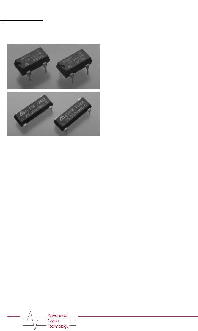
Epson SG531P 16.0000M, SG531P 16.2570M, SG531P 20.0000M, SG531P 20.2752M, SG531P 23.5870M Datasheet
...
Crystal Oscillators - Seiko Epson
H C M O S / T T L D UA L I N L I N E P L A S T I C F U L L S I Z E S G - 5 1 / H A L F S I Z E S G - 5 3 1
SG-51/Half Size SG531
SG531
SG51
Features
•Frequency range 1.025MHz-125.0MHz
•Cylindrical type AT cut crystal quartz built in, thereby assuring high reliability
•Suitable for automatic insertion
•Use of CMOS IC enables reduction of current consumption
•Output load 10LSTTL/30-50pF
•Available with output enable and standby functions - SG51P and SG531P series
•Pin compatible with 8 pin and 14 pin metal can versions
•Packaged in plastic DIP package saves board space
•Extensive stock holding on SG531 series
Specifications
|
|
Item |
Symbol |
|
Specifications |
|
Remarks |
||||
|
|
|
|
SG-51P/531P |
SG-51PTJ/531 PTJ |
SG-51PH/531PH |
|
|
|||
|
|
|
|
|
|
|
|
|
|||
|
|
|
|
|
|
|
|
|
|||
Output frequency range |
fo |
1.0250MHz to |
26.0001MHZ to 66.6667MHZ |
|
|
||||||
|
|
|
|
26.0000MHz |
|
|
|
|
|
|
|
Power source |
|
Max. supply voltage |
Vpp -GND |
|
-0.3V to +7.0V |
|
|
|
|||
|
|
|
|
|
|
|
|
|
|
||
voltage |
|
Operating voltage |
VDD |
|
5.0V±0.5V |
|
|
|
|||
|
|
|
|
|
|
|
|
|
|
||
Temperature |
Storage temp. |
TSTG |
-55°C to +125°C |
-55°C to +100°C |
|
|
|||||
range |
Operating temp. |
TOPR |
|
-10°C to +70°C |
|
|
|
||||
Soldering condition (lead part) |
TSOL |
|
Under 260°C within 10 sec. |
|
Don’t heat up the package more than 150°C |
||||||
|
|
|
|
|
|
|
|
|
|
||
Frequency stability |
|
f/fo |
|
B: ±50ppm |
|
-10°C to +70°C |
|||||
|
|
|
|
|
C: ±100ppm |
|
B Type is possible up to 55.0MHz |
||||
Current consumption |
lop |
23mA MAX. |
35mA MAX. |
|
No load condition |
||||||
|
|
|
|
|
|
|
|
|
|
|
|
Duty |
C-MOS level |
Tw/T |
40% to 60% |
– |
40% to 60% |
1.2VDD |
level |
||||
|
|
TTL level |
|
45% to 55% |
– |
1.4V level |
|||||
Output voltage |
|
VOH |
VDD - 0.4V MIN. |
2.4V MIN. |
|
|
VDD -0.4V MIN. |
|
|
||
|
|
|
(IOH) |
-400µA |
|
|
-4µA |
|
|
||
|
|
|
VOL |
|
0.4V MAX. |
|
|
|
|||
|
|
|
(IOL ) |
16mA |
8mA |
|
|
4mA |
|
|
|
|
|
|
|
|
|
|
|
|
|
|
|
Output load |
C-MOS |
CL |
50pF MAX. |
– |
50pF MAX. |
|
|
||||
condition (fan out) |
TTL |
N |
10TTL MAX. |
5TTL MAX. |
– |
|
|
||||
Output enable/disable input voltage |
VIH |
2.0V MIN |
3.5V MIN. |
|
|
2.0V MIN. |
IIH = 1µ A MAX. (OE=VDD) |
||||
|
|
|
VIL |
0.8V |
1.5V MAX. |
|
|
0.8V MAX. |
IIL =-100µ A MIN. (OE=GND), PTJ: -500µA |
||
Output disable current |
IOE |
12mA MAX. |
28mA MAX. |
20mA MAX. |
OE=GN |
||||||
Output |
|
C-MOS level |
TTLH |
8nsec.MAX |
5nsec. MAX |
|
|
7nsec. MAX. |
C-MOS load : 20% to 80% VDD |
||
rise time |
|
TTL level |
|
|
TTL load : 0.4V to 2.4V |
||||||
|
|
|
|
|
|
|
|||||
|
|
|
|
|
|
|
|
|
|
||
Output |
C-MOS level |
TTHL |
8nsec.MAX |
5nsec. MAX |
7nsec. MAX. |
C-MOS load : 80% to 20% VDD |
|||||
fall time |
TTL level |
TTL load : 2.4V to 0.4V |
|||||||||
|
|
|
|
|
|
||||||
Oscillation start up time |
tOSC |
4msec. MAX. |
10msec. MAX. |
More than for 1ms until VDD =0V to 4.5V |
|||||||
|
|
|
Time at 4.5V to be 0sec. |
||||||||
|
|
|
|
|
|
|
|
|
|||
|
|
|
|
|
|
|
|
|
|
|
|
Aging |
|
fa |
|
±5ppm/year MAX. |
|
Ta = 25°C, VDD |
=5V, first year |
||||
Shock resistance |
|
S.R. |
|
±20ppm MAX. |
|
Drop Test of three times on hard board from |
|||||
|
|
|
|
|
|
|
|
|
75cm height or excitation test with 3000G x |
||
|
|
|
|
|
|
|
|
|
0.3ms x 1/2 sine wave in 3 directions. |
||
|
|
|
|
|
|
|
|
|
|
|
|
Notes |
|
|
|
|
|
|
|
|
|
||
•Unless otherwise stated, characteristics (specifications) shown in the above table are based on the rated operating temperature and voltage condition.
•External by-pass capacitor is recommended.
TEL: +44 1635 528520 FAX: +44 1635 528443
 Loading...