


Voltage
LowOperation
Products
PF110-10
SCI7661COA/MOA
DC-DC Converter
●95% Typical Power Efficiency
●Doubled or Tripled Output Voltage
●Internal Voltage Regulator
■ DESCRIPTION
The SCI7661COA/MOACMOS DC-DC Converter features high operational performance with low power dissipation. It consists of two major parts: the booster circuitry and the regulator circuitry. The booster generates a doubled output voltage(–2.4 to –12V) or tripled output voltage(–3.6 to –18V) from the input (–1.2 to –6V). The regulator is capable of setting the output to any desired voltage. The regulated voltage can be given one of the three threshold temperature gradients.
■FEATURES
●High performance with low power dissipation
●Simple conversion of VIN (–5V) to |VIN| (+5V), 2 |VIN| (+10V), 2VIN (–10V) or 3VIN(–15V)
●On-chip output voltage regulator
●Power conversion efficiency–Typ. 95%
●Temperature gradient for LCD power supply – 0.1% / °C, 0.4%/°C or 0.6%/ °C
●Power off by external signals – Stationary current at power off – Max. 2 μA
●Cascade connection–two device connected: VIN=–5V, VOUT=–20V
●On-chip C'–R oscillator
●Package .................................... SCI7661C0A: DIP-14pin(plastic)
SCI7661M0A: SOP5-14pin(plastic)
SCI7661MAA: SSOP2-16pin(plastic)
■ BLOCK DIAGRAM
VDD |
|
|
|
|
|
|
|
|
OSC1 |
CR |
Reference Voltage |
|
|
Temperature Gradient |
|
|
|
OSC2 |
Oscillator |
Generator |
Voltage Regulator |
Circuit |
TC1 |
|||
|
|
|||||||
VIN |
|
|
||||||
|
T |
TC2 |
||||||
CAP1– |
Voltage |
Select |
||||||
|
||||||||
CAP1+ |
Converter |
|
||||||
(I) |
Poff |
|||||||
CAP2– |
|
|||||||
|
|
RV |
||||||
|
Voltage |
|
|
|
|
|
||
|
|
|
|
|
|
Vreg |
||
CAP2+ |
Converter |
|
|
|
|
|
||
|
(II) |
|
|
|
|
|
|
|
|
|
|
|
|
|
|
Vout |
|
|
Booster |
|
|
Regurator |
|
|
|
SCI7661COA/MOA
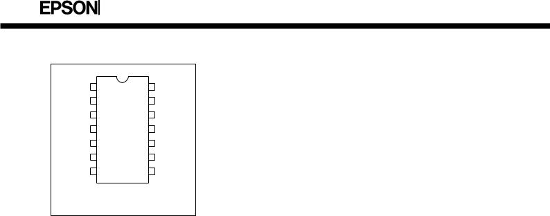
■ PIN CONFIGURATION
CAP1+ |
1 |
14 |
VDD |
|
CAP1- |
2 |
13 |
OSC1 |
|
CAP2+ |
3 |
12 |
OSC2 |
|
CAP2- |
4 |
11 |
|
|
Poff |
|
|||
TC1 |
5 |
10 |
RV |
|
TC2 |
6 |
9 |
Vreg |
|
VIN |
7 |
8 |
Vout |
|
The same pin configuration in DIP and SOP
■ PIN DESCRIPTION
Pin name |
No. |
Function |
|
|
|
|
|
CAP1+, CAP1- |
1, |
2 |
Terminal for connection of capacitor for doubler |
CAP2+, CAP2- |
3, |
4 |
Terminal for connection of capacitor for tripler |
TC1, TC2 |
5, |
6 |
Temperature gradient selection terminal |
VIN |
7 |
|
Power supply terminal(negative, system supply |
|
|
|
GND) |
VOUT |
8 |
|
Output terminal at tripling |
Vreg |
9 |
|
Regulated voltage output terminal |
RV |
10 |
Regulated voltage control terminal |
|
Poff |
11 |
Vreg output ON/OFF control terminal |
|
OSC2, OSC1 |
12, |
13 |
Oscillation resistor connection terminal |
VDD |
14 |
Power supply terminal(positive system supply |
|
|
|
|
VCC) |
■ ABSOLUTE MAXIMUM RATINGS
(VDD=0V)
Rating |
Symbol |
Min. |
Max. |
Unit |
Remark |
|||
|
|
|
|
|
|
|
|
|
Input supply voltage |
VI |
-20/N |
0.5 |
V |
N=2 : Doubler |
|||
N=3 : Tripler |
||||||||
|
|
|
|
|
OSC1, |
|
|
|
Input terminal voltage |
VI |
VIN-0.5 |
0.5 |
V |
Poff |
|||
VOUT-0.5 |
0.5 |
V |
TC1, TC2, RV |
|||||
|
|
|||||||
Output voltage |
VO |
-20.0 |
|
V |
|
|
|
|
Allowable loss |
Pd |
|
300 |
mW |
|
|
|
|
Operating temperature |
Topr |
-30 |
85 |
°C |
Plastic package |
|||
Storage temperature |
Tstg |
-55 |
150 |
°C |
|
|
|
|
Soldering temperature and time |
Tsol |
260°C, 10s(at lead) |
- |
|
|
|
||
Note: When this IC is soldered in the solder-reflow process, be sure to maintain the reflow furnace at the curve shown in "Fig. 1-5 Reflow Furnace Temperature Curve" of this DATA BOOK. And this IC can not be exposed to high temperature of the solder dipping.
■ ELECTRICAL CHARACTERISTICS
|
|
|
|
|
|
|
|
(VDD = 0V, VIN=-5V, Ta=-30 to 85°C) |
|
|
|
|
|
|
|
|
|
|
|
Characteristic |
|
Symbol |
Min. |
Typ. |
Max. |
Unit |
Condition |
|
|
|
|
|
|
|
|
|
|
|
|
Input supply voltage |
|
VI |
-6.0 |
|
-1.2 |
V |
|
|
|
Output voltage |
|
VO |
-18.0 |
|
|
V |
|
|
|
|
Vreg |
-18 |
|
-2.6 |
V |
RL=¥, RRV=1MΩ , |
|
||
|
|
|
VO=-18V |
|
|||||
|
|
|
|
|
|
|
|
|
|
Regulator operating voltage |
|
VOUT |
-18.0 |
|
-3.2 |
V |
|
|
|
Booster current consumption |
|
Iopr1 |
|
60 |
100 |
µA |
RL=¥, ROSC=1MΩ |
|
|
Regulator current |
|
Iopr2 |
|
50 |
12.0 |
µA |
RL=¥, RRV=1MΩ |
|
|
consumption |
|
|
VOUT=-15V |
|
|||||
|
|
|
|
|
|
|
|
||
Stationary current |
|
IQ |
|
|
2.0 |
µA |
TC2=TC1=VOUT, RL=¥ |
|
|
Oscillation frequency |
|
fosc |
16 |
20 |
24 |
kHz |
ROSC=1MΩ |
|
|
Output impedance |
|
ROUT |
|
150 |
200 |
Ω |
IOUT=10mA |
|
|
Booster power conversion |
|
Peff |
90 |
95 |
|
% |
IOUT=5mA |
|
|
efficiency |
|
|
|
||||||
|
|
|
|
|
|
|
|
|
|
|
|
|
|
|
|
|
|
|
|
Regulated output voltage |
|
DVreg |
|
|
0.2 |
|
%/V |
-18V<VOUT<-8V, |
|
fluctuation |
|
DVOUT•Vreg |
|
|
Vreg=-8V, RL=¥, Ta=25°C |
|
|||
|
|
|
|
|
|
||||
2

|
|
|
|
|
|
|
|
|
|
|
|
|
|
|
|
|
|
|
|
SCI7661COA/MOA |
||||
|
|
|
|
|
|
|
|
|
|
|
|
|
|
|
|
|
|
|
|
|
|
|
|
|
|
|
|
|
|
|
|
|
|
|
|
|
|
|
|
|
|
|
|
|
|
|
|
|
|
|
Characteristic |
|
Symbol |
|
|
Min. |
|
Typ. |
|
Max. |
Unit |
|
|
|
|
Condition |
|
|||||||
|
|
|
|
|
|
|
|
|
|
|
|
|
|
|
|
|
|
|
|
|
|
|||
|
Regulated output load |
|
|
DVreg |
|
|
|
|
|
|
|
|
|
|
|
VOUT=-15V, Vreg=-8V, |
|
|||||||
|
|
|
|
|
|
|
5 |
|
|
|
Ω |
Ta=25°C |
|
|
|
|
|
|||||||
|
fluctuation |
|
|
DIOUT |
|
|
|
|
|
|
|
0<IOUT<10mA, TC1=VDD |
|
|||||||||||
|
|
|
|
|
|
|
|
|
|
|
|
|
|
|||||||||||
|
|
|
|
|
|
|
|
|
|
|
|
|
|
|
|
TC2=VOUT |
|
|
|
|||||
|
Regulated output saturation |
|
|
|
|
|
|
|
|
|
|
|
|
Ω |
RSAT=D(Vreg—V OUT)/DIOUT |
|
||||||||
|
|
|
RSAT |
|
|
|
|
5 |
|
|
|
0<IOUT<10mA, RV=VDD, |
|
|||||||||||
|
resistance |
|
|
|
|
|
|
|
|
|
|
|||||||||||||
|
|
|
|
|
|
|
|
|
|
|
|
|
|
|
Ta=25°C |
|
|
|
|
|
||||
|
|
|
|
|
|
|
|
|
|
|
|
|
|
|
|
|
|
|
|
|
||||
|
|
|
|
|
|
|
|
|
|
|
|
|
|
|
|
|
|
|||||||
|
|
|
|
VRV0 |
|
-2.3 |
|
-1.5 |
|
|
-1.0 |
V |
TC2=VOUT, TC1=VDD, Ta=25°C |
|
||||||||||
|
Reference voltage |
|
|
VRV1 |
|
-1.7 |
|
-1.3 |
|
|
-1.1 |
V |
TC2=TC1=VOUT, Ta=25∞ C |
|
||||||||||
|
|
|
|
VRV2 |
|
-1.1 |
|
-0.9 |
|
|
-0.8 |
V |
TC2=VDD, TC1=VOUT, Ta=25°C |
|
||||||||||
|
|
0 |
|
|
|
|
|
|
|
|
|
%/°C |
|
|
|
|
| Vreg(50°C) | - | Vreg(0°C) | |
|
||||||
|
|
|
|
CT |
|
-0.25 |
|
-0.1 |
|
|
-0.06 |
CT = |
|
|
|
|
|
|
|
|||||
|
Temperature Gradient |
|
|
|
|
|
|
50°C-0°C |
|
|||||||||||||||
|
|
|
CT4 |
|
-0.5 |
|
-0.4 |
|
|
-0.3 |
%/°C |
|
|
|
|
|
||||||||
|
|
|
|
CT2 |
|
-0.7 |
|
-0.6 |
|
|
-0.5 |
%/°C |
´ |
|
|
|
1 |
|
´100 |
|
|
|||
|
|
|
|
|
|
|
|
| Vreg(25°C) | |
|
|
||||||||||||||
|
|
|
|
|
|
|
|
|
|
|
|
|
|
|
|
|
|
|
|
|||||
|
Input leakage current |
|
|
IL |
|
|
|
|
|
|
|
2.0 |
µA |
Poff, TC1, TC2, OSC1, RV pins |
|
|||||||||
|
|
|
|
|
|
|
|
|
|
|
|
|
|
|
|
|
|
|
|
|
|
|
||
■ RECOMMENDED OPERATING CONDITIONS |
|
|
|
|
|
|
|
|
|
(Ta=-30 to 85°C) |
||||||||||||||
|
|
|
|
|
|
|
|
|
|
|
|
|
|
|
|
|
|
|
|
|||||
|
Condition |
|
|
Symbol |
|
|
Min. |
|
Max. |
|
|
Unit |
|
|
|
|
|
Remark |
|
|||||
|
|
|
|
VSTA1 |
|
|
|
|
|
|
-1.2 |
|
|
V |
|
|
|
ROSC=1MΩ , C3≥10µF*1 |
|
|||||
|
Booster start voltage |
|
|
|
|
|
|
|
|
|
|
|
|
|
CL/C3≤ 1/20, Ta=-20 to 85°C |
|
||||||||
|
|
|
|
VSTA2 |
|
|
|
|
|
|
-2.2 |
|
|
V |
|
|
|
ROSC=1MΩ |
|
|
|
|||
|
Booster stop voltage |
|
|
VSTP |
|
|
-1.2 |
|
|
|
|
|
V |
|
|
|
ROSC=1MΩ |
|
|
|
||||
|
Output load resistance |
|
|
RL |
|
RL Min.*2 |
|
|
|
|
|
Ω |
|
|
|
|
|
|
|
|
||||
|
Output load current |
|
|
IOUT |
|
|
|
|
|
|
20 |
|
|
mA |
|
|
|
|
|
|
|
|
||
|
Oscillation frequency |
|
|
fOSC |
|
|
10 |
|
|
30 |
|
|
kHz |
|
|
|
|
|
|
|
|
|||
|
Extarnal resistance for |
|
|
ROSC |
|
|
680 |
|
|
2000 |
|
|
kΩ |
|
|
|
|
|
|
|
|
|||
|
oscillation |
|
|
|
|
|
|
|
|
|
|
|
|
|
|
|
|
|||||||
|
|
|
|
|
|
|
|
|
|
|
|
|
|
|
|
|
|
|
|
|
|
|
|
|
|
Capasitor for booster |
|
|
C1, C2, C3 |
|
3.3 |
|
|
|
|
|
µF |
|
|
|
|
|
|
|
|
||||
|
Regulated output adjustable |
|
|
RRV |
|
|
100 |
|
|
1000 |
|
|
kΩ |
|
|
|
|
|
|
|
|
|||
|
resistance |
|
|
|
|
|
|
|
|
|
|
|
|
|
|
|
|
|||||||
|
|
|
|
|
|
|
|
|
|
|
|
|
|
|
|
|
|
|
|
|
|
|
|
|
|
|
|
|
|
|
|
|
|
||||||||||||||||
|
*1: Recommended circuity in low voltage operation is |
*2: RL Min. depends on input voltage as shown below. |
||||||||||||||||||||||
|
shown below. |
|
|
|
|
|
|
|
|
|
|
|
|
|
|
|
|
|
|
|
|
|
|
|
(VIN=-1.2V ~ -2.2V)
=C1=10µF |
1 |
14 |
|
|
|
|
+ |
|
|
|
|
||
|
|
|
|
|||
- |
2 |
13 |
ROSC= |
|
|
|
+ |
3 |
12 |
1MΩ |
RL |
CL |
|
- |
4 |
11 |
|
|
|
|
C2=10µF |
5 |
10 |
|
|
|
|
|
|
|
|
|||
|
6 |
9 |
|
|
|
|
|
7 |
8 |
|
|
|
|
+ -
C3=22µF
D1(VF(IF=1mA)) ≤ 0.6v
RL Min.(kΩ )
5 |
|
|
|
|
|
|
|
|
|
|
|
|
|
|
|
|
|
|
|
|
|
|
|
|
VSTA2 |
|
|
||
|
|
|
|
|
|||||
4 |
|
|
|
|
VSTA1 |
|
|
||
|
|
|
|
|
|
|
|
|
|
3 |
|
|
|
|
|
|
|
|
|
|
|
|
|
|
|
|
|
|
|
2 |
|
|
|
|
|
|
|
|
|
|
|
|
|
|
|
|
|
|
|
1 |
|
|
|
|
|
|
|
|
|
|
|
|
|
Triple |
|
||||
|
|
|
|
||||||
|
|
|
|
|
|
|
|
|
|
Double
0
0 1.5 2 3 4 5 6 VIN(V)
3
 Loading...