


 Loading...
Epson S1D15G00D00*100, S1D15G00D01*100, S1D15G00D03*100, S1D15G00D05*100, S1D15G00D06*100 Schematic [ru]
...MF1387-04
S1D15G00 Series
Rev. 1.0
“Seiko Epson is neither licensed nor authorized to license its customers under one or more patents held by Motif Corporation to use this integrated circuit in the manufacture of liquid crystal display modules. Such license, however, may be obtained directly from MOTIF by writing to: Motif, Inc., c/o In Focus Systems, Inc., 27700A SW Parkway Avenue, Wilsonville, OR 97070-9215, Attention: Vice President Corporate Development.”
Seiko Epson Corporation 2001, All rights reserved.
Rev. 1.0
|
Contents |
|
1. |
DESCRIPTION .................................................................................................................................................. |
1 |
2. |
FEATURES........................................................................................................................................................ |
1 |
3. |
BLOCK DIAGRAM ............................................................................................................................................. |
2 |
4. |
PIN LAYOUT ..................................................................................................................................................... |
3 |
5. |
LIST OF DEVICE MODELS ............................................................................................................................... |
3 |
6. |
PIN COORDINATE ............................................................................................................................................ |
4 |
7. |
PIN DESCRIPTION ........................................................................................................................................... |
6 |
8. |
FUNCTIONAL DESCRIPTION ........................................................................................................................ |
11 |
9. |
COMMANDS ................................................................................................................................................... |
30 |
10. |
ABSOLUTE MAXIMUM RATING ..................................................................................................................... |
42 |
11. |
ELECTRIC CHARACTERISTICS .................................................................................................................... |
43 |
12. |
MPU INTERFACES (EXAMPLES FOR YOUR REFERENCE) ....................................................................... |
53 |
13. |
PERIPHERAL CONNECTION EXAMPLES .................................................................................................... |
58 |
14. |
EEPROM INTERFACE .................................................................................................................................... |
60 |
15. |
CAUTIONS ...................................................................................................................................................... |
61 |
– i – |
Rev. 1.0 |

S1D15G00 Series
1. DESCRIPTION
S1D15G00 series are the LCD drivers equipped with the liquid crystal drive power circuit to realize color display with one chip.
S1D15G00 can be directly connected to the MPU bus to store parallel or serial gray-scale display data from MPU on the built-in RAM and to generate liquid crystal drive signals independent from MPU. S1D15G00 generates 396 segment outputs and 160*1 common outputs for driving liquid crystal. It incorporates the display RAM with capacity of 396 × 168 × 4 (16 grayscale). A single dot of pixel on the liquid crystal panel corresponds to 4 bits of the built-in RAM, enabling to display 132 (RGB) × 160 pixels with one chip.
Read or write operations from MPU to the display RAM can be performed without resorting to external actuating clock signals. S1D15G00 allows you to run the display system of high performance and handy equipment at the minimum power consumption thanks to its low-power liquid crystal drive power circuit and oscillation circuit. *1 : The S1D15G00D10*100 generates 300 segment
outputs and 120 common outputs. It incorporates the display RAM with 300 × 168 × 4 capacity and displays 100 (RGB) × 120 pixels.
2. FEATURES
• Number of liquid crystal-drive outputs:
396 segment outputs and 160 common outputs.
•Low cross talk by frame rate modulation.
•256 color from 4096-color display or full 4096-color display.
When 256 color from 4096-color display is selected: 8 gray-scale for red and green and 4 gray-scale for blue (intermediate tone is selected with the command). When 4096-color display is selected: 16 gray-scale for red, green and blue.
•Direct data display with display RAM
(When the LCD is set to normally black) RAM bit Data “0000” ... OFF (Black)
“1111” ...ON (Maximum RGB display) (Normally black LCD, using "inverse display" command)
•Partial display function: You can save power by limiting the display space. This function is most suited for handy equipment in the standby mode.
•Display RAM : 396 × 168 × 4 = 266,112 bits.*1
*1: The S1D15G00D10*000 has RAM of 300 × 120
×4 = 144,000 bits.
•MPU interface: S1D15G00 can be directly connected to both of the 8/16-bit parallel 80 and 68 series MPU. Two type serial interface are also available.
•3 pins serial : CS, SCL and SI (D/C + 8-bit data)
•4 pins serial : CS, SCL, SI and A0
•Abundant command functions: Area scroll function, automatic page & column increment function, display direction switching function and power circuit control function.
•Built-in liquid crystal drive power circuit: S1D15G00 is equipped the charge pump booster circuit, voltage follower circuit and electric volume control circuit.
•Oscillation circuit with built-in high precision CR (external clock signals acceptable)
•EEPROM interface functions
•Low current consumption
500µ A (Conditions: S1D15G00D01B100, VDD = VDDI = 3.0V, frame frequency 130Hz, V2 = 6.0V, all display RAM data is “0”)
• Supply voltage
Power for input/output system power: VDDI–GND=1.7V to 3.6V
Power for internal circuit operation: VDD–GND=2.6V to 3.6V Reference power for booster circuit: VDD2–GND=2.6V to 3.6V
Power for liquid crystal drive: V3–MV3=12.0V to 21.0V
•Wider operational range: –40° C to 85° C.
•Shipping from: Chip with gold bump. COF.
•Note that the radiation resistant design or light resistance design in strict sense is not employed for S1D15G00.
Rev. 1.0 |
EPSON |
1 |
S1D15G00 Series
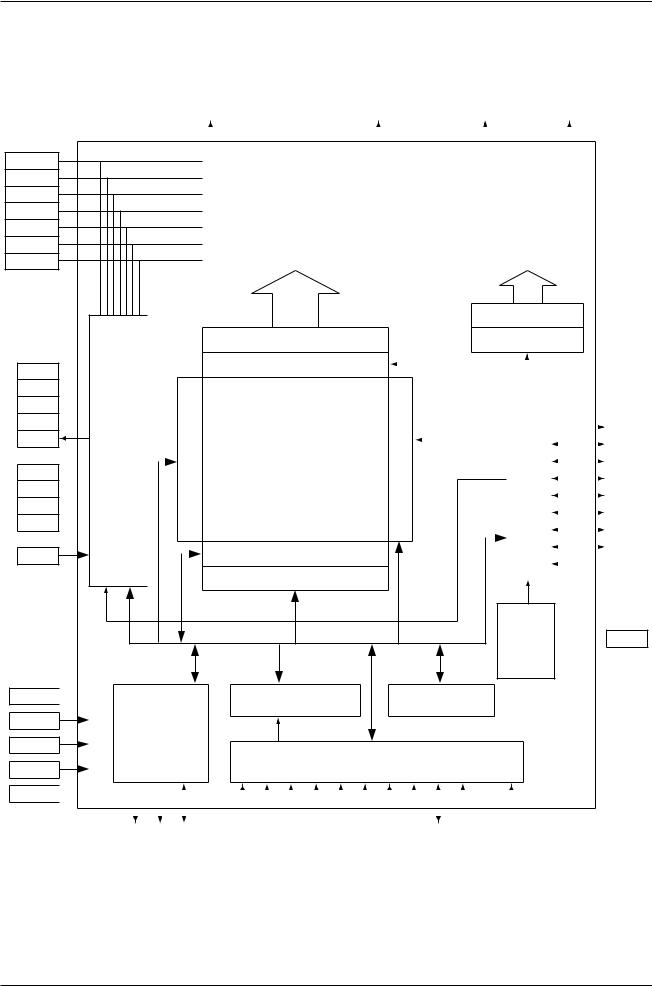
3. BLOCK DIAGRAM
V3
V2
V1
VC
MV1
MV2(GND)
MV3
CAP1+  CAP1–
CAP1–  CAP2+
CAP2+ 
CAP2– 
VCLS
CAP4+  CAP4–
CAP4–  CAP5+
CAP5+  CPP5–
CPP5– 
VDD2
VDD3 to 5 

VDD
VDDI
GND
GND2 to 4 

SEG1 |
• • • • • • • • • • • • • • • • • • • • |
SEG396 |
|
COM1 |
• • • • • • • • |
COM160 |
|
|
|
|
|
||
|
|
|
|
|
|
|
|
|
|
|
|
|
|
|
SEG Drivers |
|
|
COM Drivers |
||
|
|
|
||||
|
||||||
|
|
|
|
|
|
|
|
|
|
|
|
|
|
|
|
|
|
|
|
|
|
COM decoder |
|
|
|
|
|
|||||||
|
|
|
|
|
|
|
|
|
|
|
|
|||||||||
|
|
|
|
|
SEG decoder |
|
|
Shift register |
|
|
|
|
|
|||||||
Power circuit |
|
|
|
Pageaddress |
Display data latch |
|
|
|
|
|
|
|
|
|
|
|
|
|
|
|
|
|
|
|
|
|
|
|
|
|
|
|
|
|
|
|
|
|
|||
|
|
|
Blockaddress |
|
|
|
|
|
|
|
|
|
|
|
|
|
|
|||
|
|
|
|
|
|
|
|
|
|
|
|
|
|
|
|
|
|
|||
|
|
|
|
|
|
|
|
timingDisplaysignal circuitgeneration |
|
|
|
DOFF |
||||||||
|
|
|
|
|
|
|
|
|
|
|
|
|
|
|
|
|
|
SLP |
||
|
|
|
|
|
DDRAM |
|
|
|
|
|
|
|
|
|
|
YSCL |
||||
|
|
|
|
|
396 x 168 x 4 |
|
|
|
|
|
|
|
|
|
|
F1,F2 |
||||
|
|
|
|
|
|
|
|
|
|
|
|
|
|
|
|
|
|
CA |
||
|
|
|
|
|
|
|
|
|
|
|
|
|
|
|
|
|
|
FR |
||
|
|
|
|
|
|
|
|
|
|
|
|
|
|
|
|
|
|
|||
|
|
|
|
|
|
|
|
|
|
|
|
|
|
|
|
SYNC |
||||
|
|
|
|
|
|
|
|
|
|
|
|
|
|
|
|
|||||
|
|
|
|
|
I/O buffer |
|
|
|
|
|
|
|
|
|
|
|
|
CL |
||
|
|
|
|
|
|
|
|
|
|
|
|
|
|
|
|
|
||||
|
|
|
|
|
|
|
|
|
|
|
|
|
|
|
|
|
|
|
|
|
|
|
|
|
|
|
|
|
|
|
|
|
|
|
|
|
|
|
|
|
|
|
|
|
|
|
|
|
|
|
|
|
|
|
|
|
|
|
|
|
|
|
|
|
|
|
|
|
|
|
|
|
|
|
|
|
|
|
|
M/S |
|||
|
|
|
|
|
Column address |
|
|
|
|
|
|
|
|
|
|
|
|
|||
|
|
|
|
|
|
|
|
|
|
|
|
|
|
|
|
|
||||
|
|
|
|
|
|
|
|
|
|
|
|
|
|
|
|
|
|
|
|
|
|
|
|
|
|
|
|
|
|
|
|
|
|
|
|
|
|
|
|
|
|
Oscillation  CLS
CLS
circuit
Command decoder |
Bus holder |
EEPROM interface
MPU interface
|
|
|
|
|
|
|
|
|
|
|
|
|
|
|
|
|
|
|
|
|
|
|
|
|
|
|
|
|
|
|
|
|
|
|
|
|
|
|
|
|
|
|
|
|
|
|
|
|
|
|
|
|
|
|
|
|
|
|
|
|
|
|
|
|
|
|
|
|
|
|
|
|
|
|
|
|
|
|
|
|
|
|
|
|
|
|
|
|
|
|
|
|
|
|
|
|
|
|
|
|
|
|
|
|
|
|
|
|
|
|
|
|
|
|
|
|
|
|
|
|
|
|
|
|
|
|
|
|
|
|
|
RESET |
|
CLOCK |
|
SDA |
|
|
RES |
|
|
RD(E) |
|
|
WR(R/W) |
|
CS |
|
A0 |
|
IF1,IF2,IF3 |
|
SI |
|
SCL |
|
D15 to D0 |
|
TEST |
|
SRCM |
||||||||||||||
|
|
|
|
|
|
|
|
|
|
|
|
|
|||||||||||||||||||||||||||||||
|
|
|
|
|
|
|
|
|
|
||||||||||||||||||||||||||||||||||
|
|
|
|
|
|
|
|
|
|
|
|||||||||||||||||||||||||||||||||
|
|
|
|
|
|
|
|
|
|
|
|
|
|
|
|
|
|
|
|||||||||||||||||||||||||
|
|
|
|
|
|
|
|
|
|
|
|
|
|
|
|
|
|
|
|
|
|
|
|
|
|
|
|
||||||||||||||||
|
|
|
|
|
|
|
|
|
|
|
|
|
|
|
|
|
|
|
|
|
|
|
|
|
|
|
|
|
|
|
|
|
|
|
|
|
|
||||||
|
|
|
|
|
|
|
|
|
|
|
|
|
|
|
|
|
|
|
|
|
|
|
|
|
|
|
|
|
|
|
|
|
|
|
|
|
|
||||||
|
|
|
|
|
|
|
|
|
|
|
|
|
|
|
|
|
|
|
|
|
|
|
|
|
|
|
|
|
|
|
|
|
|
|
|
|
|
|
|
|
|
||
|
|
|
|
|
|
|
|
|
|
|
|
|
|
|
|
|
|
|
|
|
|
|
|
|
|
|
|
|
|
|
|
|
|
|
|
|
|
|
|
|
|
|
|
2 |
EPSON |
Rev. 1.0 |
S1D15G00 Series
4. PIN LAYOUT
792 |
|
205 |
|
Die No. |
Y |
X |
|
(0,0) |
|||
|
|||
1 |
|
204 |
Chip size |
25.04 mm × 2.70 mm |
|
|
|
|
|
Chip thickness |
725 µ m± 25 µ m (for reference) |
|||||
Die No. |
See Section 5 “List of Device Models.” |
|||||
Potential on board |
GND |
|
|
|
|
|
Bump size |
Tolerance: bump of the shorter side ± 3 µ m, bump of the longer side ± 4 µ m (reference) |
|||||
|
Driver output side: |
30 µ m × |
137 µ m |
|||
|
Driver input side: |
82 µ m × |
109 µ m |
|||
Bump pitch |
Driver output side: 42 µ m |
|
|
|
|
|
|
I/O signal line side:100 µ m min. |
|||||
Bump height |
22.5 µ m± 4 µ m (for reference) : S1D15G00D0*B0 |
|||||
Alignment coordinate |
|
|
|
|
|
|
|
1 (–11974.2, –639.2) |
|
|
|
|
|
|
2 (12091.8, –730.4) |
|
|
|
|
|
Mark size |
a = 80 µ m |
|
|
|
|
|
|
b = 20 µ m |
|
|
|
|
|
|
|
|
|
b |
a |
|
|
|
|
|
|
|
|
|
|
|
|
|
|
|
5. LIST OF DEVICE MODELS
|
|
Output |
V2 voltage |
Access |
MPU RAM |
Frame frequency |
|
Model name |
Die No. |
control resistor |
/built-in oscillation |
||||
count |
to EEPROM |
read |
|||||
|
|
External/Internal |
frequency |
||||
|
|
|
|
|
|||
S1D15G00D00*100 |
D15G0D0B |
Segment: 396 |
Internal only |
|
Unable to read |
130 Hz |
|
(#) |
|
Common: 160 |
(voltage electronically |
|
|
/41.6 kHz |
|
S1D15G00D05*100 |
D15G0D5B |
|
controlled via |
|
Read enabled |
|
|
|
|
|
electronic volume) |
|
|
|
|
S1D15G00D01*100 |
D15G0D1B |
|
External only |
× |
Unable to read |
|
|
(#) |
|
|
(voltage controlled |
|
|
|
|
|
|
|
|
|
|
|
|
S1D15G00D06*100 |
D15G0D6B |
|
via VR pin |
|
Read enabled |
|
|
|
|
|
resistance) |
|
|
|
|
S1D15G00D03*100 |
D15G0D3B |
|
External only |
× |
Unable to read |
180 Hz |
|
(#) |
|
|
(voltage controlled |
|
|
/57.6 kHz |
|
S1D15G00D08*100 |
D15G0D8B |
|
via VR pin |
|
Read enabled |
|
|
|
|
|
resistance) |
|
|
|
|
S1D15G00D10*100 |
D15G0DAB |
Segment: 300 |
External only (voltage |
× |
Unable to read |
130 Hz |
|
(#) |
|
Common: 120 |
via VR pin resistance) |
|
|
/31.2 kHz |
(Note)
For “unable to read” models in the above diagram, the MPU cannot read the RAM. If the RAM must be read, use “read enabled” models.
(#) : These models will be discontinued.
Rev. 1.0 |
EPSON |
3 |

S1D15G00 Series
6. PIN COORDINATE |
|
|
|
|
|
|
|
|
|
|
|
|
|
|
|
|
|
Unit: m |
|||||
|
|
|
|
|
|
|
|
|
|
|
|
|
|
|
|
|
|
|
|
|
|
||
|
|
|
|
|
|
|
|
|
|
|
|
|
|
|
|
|
|
|
|
|
|
|
|
PAD |
Pin |
X |
Y |
|
PAD |
|
Pin |
X |
Y |
|
PAD |
|
Pin |
X |
Y |
||||||||
No. |
Name |
|
No. |
|
Name |
|
No. |
Name |
|||||||||||||||
|
|
|
|
|
|
|
|
|
|
|
|
||||||||||||
1 |
NC |
–12331 |
–1188.5 |
|
58 |
CAP1– |
–5671 |
–1188.5 |
|
115 |
GND *6 |
1569 |
–1188.5 |
||||||||||
2 |
NC |
–12211 |
|
|
|
59 |
GND2 |
–5551 |
|
|
|
116 |
VDDI *6 |
1669 |
|
|
|||||||
|
|
|
|
|
|
|
|
||||||||||||||||
3 |
V3L |
–12091 |
|
|
|
60 |
GND2 |
–5446 |
|
|
|
117 |
|
D8 |
1769 |
|
|
||||||
4 |
V3L |
–11971 |
|
|
|
61 |
GND2 |
–5341 |
|
|
|
118 |
|
D9 |
1923 |
|
|
||||||
5 |
V3L |
–11851 |
|
|
|
62 |
GND2 |
–5236.05 |
|
|
|
119 |
|
D10 |
2077 |
|
|
||||||
6 |
V2L |
–11731 |
|
|
|
63 |
GND2 |
–5131.05 |
|
|
|
120 |
|
D11 |
2231 |
|
|
||||||
7 |
V2L |
–11611 |
|
|
|
64 |
GND3 |
–5026.05 |
|
|
|
121 |
|
D12 |
2385 |
|
|
||||||
8 |
V2L |
–11491 |
|
|
|
65 |
GND3 |
–4921 |
|
|
|
122 |
|
D13 |
2539 |
|
|
||||||
9 |
V2L |
–11371 |
|
|
|
66 |
GND3 |
–4816 |
|
|
|
123 |
|
D14 |
2693 |
|
|
||||||
10 |
V1L |
–11251 |
|
|
|
67 |
|
GND |
–4711 |
|
|
|
124 |
|
D15 |
2847 |
|
|
|||||
11 |
V1L |
–11131 |
|
|
|
68 |
|
GND |
–4606 |
|
|
|
125 |
GND *6 |
3001 |
|
|
||||||
12 |
V1L |
–11011 |
|
|
|
69 |
|
GND |
–4501 |
|
|
|
126 |
VDDI *6 |
3101 |
|
|
||||||
13 |
V1L |
–10891 |
|
|
|
70 |
|
VDD3 |
–4396 |
|
|
|
127 |
|
RD |
3201 |
|
|
|||||
14 |
VCL |
–10771 |
|
|
|
71 |
|
VDD3 |
–4291 |
|
|
|
128 |
|
WR |
|
3355 |
|
|
||||
15 |
VCL |
–10651 |
|
|
|
72 |
|
VDD4 |
–4186 |
|
|
|
129 |
GND *6 |
3509 |
|
|
||||||
16 |
VCL |
–10531 |
|
|
|
73 |
|
VDD4 |
–4081 |
|
|
|
130 |
VDDI *6 |
3609 |
|
|
||||||
17 |
VCL |
–10411 |
|
|
|
74 |
TESTG |
–3976 |
|
|
|
131 |
|
IF1 |
3709 |
|
|
||||||
18 |
VCLSL |
–10291 |
|
|
|
75 |
|
VDD |
–3871 |
|
|
|
132 |
|
IF2 |
3863 |
|
|
|||||
19 |
VCLSL |
–10171 |
|
|
|
76 |
|
VDD |
–3766 |
|
|
|
133 |
|
IF3 |
4017 |
|
|
|||||
20 |
VCLSL |
–10051 |
|
|
|
77 |
|
VDDI |
–3661 |
|
|
|
134 |
GND *6 |
4171 |
|
|
||||||
21 |
VCLSL |
–9931 |
|
|
|
78 |
|
VDDI |
–3556 |
|
|
|
135 |
VDDI *6 |
4271 |
|
|
||||||
22 |
MV1L |
–9811 |
|
|
|
79 |
|
VDDI |
–3451 |
|
|
|
136 |
|
RES |
|
4371 |
|
|
||||
23 |
MV1L |
–9691 |
|
|
|
80 |
|
VDDI |
–3346 |
|
|
|
137 |
TESTH |
4525 |
|
|
||||||
24 |
MV1L |
–9571 |
|
|
|
81 |
|
|
FR |
–3235 |
|
|
|
138 |
|
MS |
4679 |
|
|
||||
25 |
MV1L |
–9451 |
|
|
|
82 |
|
YSCL |
–3081 |
|
|
|
139 |
|
VDDI |
4833 |
|
|
|||||
26 |
MV3L |
–9331 |
|
|
|
83 |
|
|
F1 |
–2927 |
|
|
|
140 |
|
VDDI |
4938 |
|
|
||||
27 |
MV3L |
–9211 |
|
|
|
84 |
|
|
F2 |
–2773 |
|
|
|
141 |
GND |
5043 |
|
|
|||||
28 |
MV3L |
–9091 |
|
|
|
85 |
|
DOFF |
|
–2619 |
|
|
|
142 |
GND |
5148 |
|
|
|||||
29 |
TESTA |
–8971 |
|
|
|
86 |
|
|
CA |
–2465 |
|
|
|
143 |
GND |
5253.05 |
|
|
|||||
30 |
TESTB |
–8871 |
|
|
|
87 |
SYNC |
–2311 |
|
|
|
144 |
GND |
5358.05 |
|
|
|||||||
31 |
TESTC |
–8771 |
|
|
|
88 |
|
SLP |
–2157 |
|
|
|
145 |
GND4 |
5463.05 |
|
|
||||||
32 |
TESTD |
–8671 |
|
|
|
89 |
|
SDA |
–2003 |
|
|
|
146 |
GND4 |
5568.05 |
|
|
||||||
33 |
TESTE |
–8571 |
|
|
|
90 |
RESET |
–1849 |
|
|
|
147 |
GND4 |
5673.05 |
|
|
|||||||
34 |
TESTF |
–8451 |
|
|
|
91 |
CLOCK |
–1695 |
|
|
|
148 |
GND4 |
5778.05 |
|
|
|||||||
35 |
TESTF |
–8336 |
|
|
|
92 |
TEST1 |
–1541 |
|
|
|
149 |
GND4 |
5883.05 |
|
|
|||||||
36 |
TESTF |
–8221 |
|
|
|
93 |
GND *6 |
–1387 |
|
|
|
150 |
|
VDD |
5988.05 |
|
|
||||||
37 |
TESTF |
–8106 |
|
|
|
94 |
VDDI *6 |
–1287 |
|
|
|
151 |
|
VDD |
6093.05 |
|
|
||||||
38 |
TESTF |
–7991 |
|
|
|
95 |
|
|
CL |
–1187 |
|
|
|
152 |
VDD5 |
6198.05 |
|
|
|||||
39 |
CAP2+ |
–7871 |
|
|
|
96 |
|
CLS |
–1033 |
|
|
|
153 |
VDD5 |
6303.05 |
|
|
||||||
40 |
CAP2+ |
–7756 |
|
|
|
97 |
GND *6 |
–879 |
|
|
|
154 |
VDD2 |
6446.05 |
|
|
|||||||
41 |
CAP2+ |
–7641 |
|
|
|
98 |
VDDI *6 |
–779 |
|
|
|
155 |
VDD2 |
6551.05 |
|
|
|||||||
42 |
CAP2+ |
–7526 |
|
|
|
99 |
|
|
CS |
|
–679 |
|
|
|
156 |
VDD2 |
6656.05 |
|
|
||||
43 |
CAP2+ |
–7411 |
|
|
|
100 |
|
|
A0 |
–525 |
|
|
|
157 |
VDD2 |
6761.05 |
|
|
|||||
44 |
CAP2– |
–7291 |
|
|
|
101 |
GND *6 |
–371 |
|
|
|
158 |
VDD2 |
6866.05 |
|
|
|||||||
45 |
CAP2– |
–7176 |
|
|
|
102 |
VDDI *6 |
–271 |
|
|
|
159 |
VDD2 |
6971.05 |
|
|
|||||||
46 |
CAP2– |
–7061 |
|
|
|
103 |
|
SCL |
–171 |
|
|
|
160 |
CAP4+ |
7113.05 |
|
|
||||||
47 |
CAP2– |
–6946 |
|
|
|
104 |
|
|
SI |
–17 |
|
|
|
161 |
CAP4+ |
7228.05 |
|
|
|||||
48 |
CAP2– |
–6831 |
|
|
|
105 |
GND *6 |
137 |
|
|
|
162 |
CAP4+ |
7343.05 |
|
|
|||||||
49 |
CAP1+ |
–6711 |
|
|
|
106 |
VDDI *6 |
237 |
|
|
|
163 |
CAP4+ |
7458.05 |
|
|
|||||||
50 |
CAP1+ |
–6596 |
|
|
|
107 |
|
|
D0 |
337 |
|
|
|
164 |
CAP4+ |
7573.05 |
|
|
|||||
51 |
CAP1+ |
–6481 |
|
|
|
108 |
|
|
D1 |
491 |
|
|
|
165 |
CAP4– |
7693.05 |
|
|
|||||
52 |
CAP1+ |
–6366 |
|
|
|
109 |
|
|
D2 |
645 |
|
|
|
166 |
CAP4– |
7808.05 |
|
|
|||||
53 |
CAP1+ |
–6251 |
|
|
|
110 |
|
|
D3 |
799 |
|
|
|
167 |
CAP4– |
7923.05 |
|
|
|||||
54 |
CAP1– |
–6131 |
|
|
|
111 |
|
|
D4 |
953 |
|
|
|
168 |
CAP4– |
8038.05 |
|
|
|||||
55 |
CAP1– |
–6016 |
|
|
|
112 |
|
|
D5 |
1107 |
|
|
|
169 |
CAP4– |
8153.05 |
|
|
|||||
56 |
CAP1– |
–5901 |
|
|
|
113 |
|
|
D6 |
1261 |
|
|
|
170 |
CAP5+ |
8273.05 |
|
|
|||||
57 |
CAP1– |
–5786 |
|
|
|
114 |
|
|
D7 |
1415 |
|
|
|
171 |
CAP5+ |
8388.05 |
|
|
|||||
|
|
|
|
|
|
|
|
|
|
||||||||||||||
4 |
EPSON |
Rev. 1.0 |

S1D15G00 Series
|
|
|
|
|
|
|
|
|
|
|
|
|
|
|
|
|
|
Unit: m |
|
|
PAD |
Pin |
X |
Y |
|
|
PAD |
Pin |
X |
Y |
|
|
PAD |
Pin |
X |
Y |
|||
|
No. |
Name |
|
|
No. |
Name |
|
|
No. |
Name |
|||||||||
|
|
|
|
|
|
|
|
|
|
|
|
|
|
||||||
|
172 |
CAP5+ |
8503.05 |
–1188.5 |
|
182 |
MV3R |
9673 |
–1188.5 |
|
192 |
V1R |
10873 |
–1188.5 |
|||||
|
173 |
CAP5+ |
8618.05 |
|
|
|
183 |
MV1R |
9793 |
|
|
|
193 |
V1R |
10993 |
|
|
||
|
|
|
|
|
|
||||||||||||||
|
174 |
CAP5+ |
8733.05 |
|
|
|
184 |
MV1R |
9913 |
|
|
|
194 |
V1R |
11113 |
|
|
||
|
175 |
CAP5– |
8853 |
|
|
|
185 |
MV1R |
10033 |
|
|
|
195 |
V1R |
11233 |
|
|
||
|
176 |
CAP5– |
8968 |
|
|
|
186 |
MV1R |
10152.9 |
|
|
|
196 |
V2R |
11353 |
|
|
||
|
177 |
CAP5– |
9083 |
|
|
|
187 |
VCLSR/VR*7 |
10273 |
|
|
|
197 |
V2R |
11473 |
|
|
||
|
178 |
CAP5– |
9198 |
|
|
|
188 |
VCR |
10393 |
|
|
|
198 |
V2R |
11593 |
|
|
||
|
179 |
CAP5– |
9313 |
|
|
|
189 |
VCR |
10513 |
|
|
|
199 |
V2R |
11713 |
|
|
||
|
180 |
MV3R |
9433 |
|
|
|
190 |
VCR |
10633 |
|
|
|
200 |
V3R |
11833 |
|
|
||
|
|
|
|
|
|
||||||||||||||
|
181 |
MV3R |
9553 |
|
|
|
191 |
VCR |
10753 |
|
|
|
|
|
|
|
|
|
|
|
|
|
|
|
|
|
|
|
|
|
|||||||||
Models other than the S1D15G00D10*000 |
|
|
|
|
|
|
|
|
|
Unit: m |
|||||||||
|
PAD |
Pin |
X |
Y |
|
|
PAD |
Pin |
X |
Y |
|
|
PAD |
Pin |
X |
Y |
|||
|
No. |
Name |
|
|
No. |
Name |
|
|
No. |
Name |
|||||||||
|
|
|
|
|
|
|
|
|
|
|
|
|
|
||||||
|
201 |
V3R |
11953 |
–1188.5 |
|
287 |
NC |
8883 |
1177 |
|
|
698 to |
NC |
*4 |
1177 |
||||
|
202 |
V3R |
12073 |
|
|
|
|
288 to |
NC |
*2 |
|
|
|
709 |
|
|
|||
|
|
|
|
|
|
|
|
|
|
||||||||||
|
|
|
|
|
|
|
|
|
|
|
|
||||||||
|
203 |
NC |
12193 |
|
|
|
299 |
|
|
|
710 |
NC |
–8883 |
|
|
||||
|
|
|
|
|
|
|
|
|
|
|
|||||||||
|
204 |
NC |
12313 |
|
|
|
300 |
NC |
8337 |
|
|
|
711 |
COM81 |
–8925 |
|
|
||
|
|
|
|
|
|
|
|
|
|||||||||||
|
205 |
NC |
12327 |
1177 |
|
301 |
SEG396 |
8295 |
|
|
|
712 |
COM82 |
–8967 |
|
|
|||
|
206 |
NC |
12285 |
|
|
|
302 |
SEG395 |
8253 |
|
|
|
713 |
COM83 |
*5 |
|
|
||
|
|
|
|
|
|
||||||||||||||
|
207 |
COM1 |
12243 |
|
|
|
303 |
SEG394 |
*3 |
|
|
|
|
to |
to |
|
|
|
|
|
208 |
COM2 |
12201 |
|
|
|
|
to |
to |
|
|
|
|
|
788 |
COM158 |
–12159 |
|
|
|
209 |
COM3 |
*1 |
|
|
|
694 |
SEG3 |
–8211 |
|
|
|
|
789 |
COM159 |
–12201 |
|
|
|
|
to |
to |
|
|
|
|
695 |
SEG2 |
–8253 |
|
|
|
|
790 |
COM160 |
–12243 |
|
|
|
|
284 |
COM78 |
9009 |
|
|
|
696 |
SEG1 |
–8295 |
|
|
|
791 |
NC |
–12285 |
|
|
||
|
285 |
COM79 |
8967 |
|
|
|
697 |
NC |
–8337 |
|
|
|
792 |
NC |
–12327 |
|
|
||
|
|
|
|
|
|
||||||||||||||
|
286 |
COM80 |
8925 |
|
|
|
|
|
|
|
|
|
|
|
|
|
|
|
|
|
|
|
|
|
|
|
|
|
|
|
|
|
|
|
|
||||
S1D15G00D10*000 |
|
|
|
|
|
|
|
|
|
|
|
|
|
|
Unit: m |
||||
|
PAD |
Pin |
X |
Y |
|
|
PAD |
Pin |
X |
Y |
|
|
PAD |
Pin |
X |
Y |
|||
|
No. |
Name |
|
|
No. |
Name |
|
|
No. |
Name |
|||||||||
|
|
|
|
|
|
|
|
|
|
|
|
|
|
||||||
|
201 |
V3R |
11953 |
–1188.5 |
|
287 |
NC |
8883 |
1177 |
|
|
698 to |
NC |
*4 |
1177 |
||||
|
202 |
V3R |
12073 |
|
|
|
|
288 to |
NC |
*2 |
|
|
|
|
709 |
|
|
||
|
|
|
|
|
|
|
|
|
|
|
|||||||||
|
|
|
|
|
|
|
|
|
|
|
|
||||||||
|
203 |
NC |
12193 |
|
|
|
|
299 |
|
|
|
|
710 |
NC |
–8883 |
|
|
||
|
|
|
|
|
|
|
|
|
|
|
|||||||||
|
204 |
NC |
12313 |
|
|
|
300 |
NC |
8337 |
|
|
|
711 |
COM61 |
–8925 |
|
|
||
|
|
|
|
|
|
|
|
|
|
|
|||||||||
|
205 |
NC |
12327 |
1177 |
|
349 |
SEG348 |
6279 |
|
|
|
712 |
COM62 |
–8967 |
|
|
|||
|
206 |
NC |
12285 |
|
|
|
350 |
SEG347 |
6237 |
|
|
|
713 |
COM63 |
*5 |
|
|
||
|
|
|
|
|
|
||||||||||||||
|
207 |
COM1 |
12243 |
|
|
|
351 |
SEG346 |
*8 |
|
|
|
|
to |
to |
|
|
|
|
|
208 |
COM2 |
12201 |
|
|
|
|
to |
to |
|
|
|
|
768 |
COM118 |
–11319 |
|
|
|
|
209 |
COM3 |
*1 |
|
|
|
649 |
SEG51 |
|
|
|
|
|
769 |
COM119 |
–11361 |
|
|
|
|
to |
to |
|
|
|
|
650 |
SEG50 |
|
|
|
|
770 |
COM120 |
–11403 |
|
|
||
|
264 |
COM58 |
9849 |
|
|
|
651 |
SEG49 |
|
|
|
|
791 |
NC |
–12285 |
|
|
||
|
265 |
COM59 |
9807 |
|
|
|
697 |
NC |
–8337 |
|
|
|
792 |
NC |
–12327 |
|
|
||
|
|
|
|
|
|
||||||||||||||
|
266 |
COM60 |
9765 |
|
|
|
|
|
|
|
|
|
|
|
|
|
|
|
|
|
|
|
|
|
|
|
|
|
|
|
|
|
|
|
|
||||
*1: You can determine the position on X coordinate from the formula “12159–42* (n–209)”, where the BUMP No. is “n”. *2: You can determine the position on X coordinate from the formula “8841–42* (n–288)”, where the BUMP No. is “n”. *3: You can determine the position on X coordinate from the formula “8211–42* (n–303)”, where the BUMP No. is “n”. *4: You can determine the position on X coordinate from the formula “-8379–42* (n–698)”, where the BUMP No. is “n”. *5: You can determine the position on X coordinate from the formula “-9009–42* (n–713)”, where the BUMP No. is “n”. *6: This pin is used to pull up or pull down nearby pins. Thus, it can’t be used for feeding power.
*7: The pin function differs among device models.
External resisting device: It functions as the primary boost voltage output pin (VCLSR). Internal resisting device: It functions as the regulator inverse input pin (VR).
*8: You can determine the position on X coordinate from formula “6145-42*(n–351)” where the Bump No. is “n”.
Rev. 1.0 |
EPSON |
5 |

S1D15G00 Series
7. PIN DESCRIPTION
7.1 Power Supply Pins
Pin name |
I/O |
Description |
Number of |
|
pins |
||||
|
|
|
||
VDDI |
Input |
They are used to connect the power for input signals. |
6 |
|
|
power |
|
|
|
VDD |
Power |
They are connected to VCC - the system power. When the system |
4 |
|
|
supply |
power is smaller than 2.6V, they must be connected another 2.6V |
|
|
|
|
or greater power supply. |
|
|
VDD2 |
Step-up |
They are used to connect the power supply for the primary step-up. |
6 |
|
|
power |
The relative magnitude of potential among the pins, namely |
|
|
|
|
VDD2≥ VDD≥ VDD1, must be observed. |
|
|
VDD3,VDD5 |
Power |
They are power supply pins on the power circuit *1. |
4 |
|
|
supply |
|
|
|
VDD4 |
Power |
They are power supply pins on the oscillation circuit *1. |
2 |
|
|
supply |
|
|
|
GND |
Power |
They are connected to the system ground. |
7 |
|
|
supply |
|
|
|
GND2, |
Power |
They are grounding pins on the power circuit *2. |
9 |
|
GND4 |
supply |
|
|
|
GND3 |
Power |
They are grounding pins on the oscillation circuit *2. |
3 |
|
|
supply |
|
|
|
V3L, V3R |
Power |
These pins are provided on the multi-level power supply for liquid |
44 |
|
V2L, V2R |
supply |
crystal drive. Relative magnitude of potential among the pins, |
|
|
V1L, V1R |
|
namely V3L(R)≥ V2L(R)≥ V1L(R)≥ VCL(R)≥ MV1L(R)≥ GND≥ MV3L(R), |
|
|
VCL, VCR |
|
must be observed. |
|
|
MV1L, MV1R |
|
When the master operation is turned on or the internal power supply |
|
|
MV3L, MV3R |
|
is turned on, predetermined voltage is output at respective pins. |
|
|
|
|
When S1D15G00 series are used in the master/slave array, they |
|
|
|
|
connect the pins on both the master and slave drivers. |
|
|
VCLSL |
Power |
They are provided on the common driver operating power supply. |
4 |
|
|
supply |
|
|
|
VCLSR,VR |
Input |
Common driver operating power supply/regulator input pins *3. |
1 |
|
|
power |
|
|
*1: Since VDD, VDD3, VDD4 and VDD5 are not internally connected, they must be externally connected to VCC - the system power.
*2: Since GND, GND2, GND3 and GND4 are not internally connected, they must be externally connected to the system GND (ground).
*3: The pin function differs among device models.
6 |
EPSON |
Rev. 1.0 |

S1D15G00 Series
7.2 Pins on Liquid Crystal Drive Power Circuit
Pin name |
I/O |
Description |
Number of |
|
pins |
||||
|
|
|
||
CAP1+ |
O |
They connect the positive going side of the primary step-up capacitor. |
5 |
|
|
|
|
|
|
CAP1– |
O |
They connect the negative going side of the primary step-up capacitor. |
5 |
|
|
|
|
|
|
CAP2+ |
O |
They connect the positive going side of the secondary step-up capacitor. |
5 |
|
|
|
|
|
|
CAP2– |
O |
They connect the negative going side of the secondary step-up capacitor. |
5 |
|
|
|
|
|
|
CAP4+ |
O |
They connect the positive going side of the tertiary step-up capacitor. |
5 |
|
CAP4– |
O |
They connect the negative going side of the tertiary step-up capacitor. |
5 |
|
CAP5+ |
O |
They connect the positive going side of the tertiary step-up capacitor. |
5 |
|
CAP5– |
O |
They connect the positive going side of the tertiary step-up capacitor. |
5 |
|
|
|
|
|
Rev. 1.0 |
EPSON |
7 |
S1D15G00 Series
7.3 MPU Interface Pins
|
Pin name |
I/O |
|
|
|
|
|
|
|
|
|
Description |
Number of |
||||||||||||||
|
|
|
|
|
|
|
|
|
|
pins |
|||||||||||||||||
|
|
|
|
|
|
|
|
|
|
|
|
|
|
|
|
|
|
|
|
|
|
|
|
|
|
|
|
|
D15 to D0 |
I/O |
They connect to the standard 8-bit or 16-bit MPU bus via the |
16 |
|||||||||||||||||||||||
|
|
|
|
|
|
|
|
|
|
8/16-bit bi-directional bus. |
|
|
|
|
|
|
|
|
|
||||||||
|
|
|
|
|
|
|
|
|
|
When the following interface is selected and the CS pin is high, the |
|
||||||||||||||||
|
|
|
|
|
|
|
|
|
|
impedance of the pin becomes high. |
|
|
|
|
|
|
|
||||||||||
|
|
|
|
|
|
|
|
|
|
1 8-bit parallel: D15-D18 are in the state of high impedance |
|
||||||||||||||||
|
|
|
|
|
|
|
|
|
|
2 Serial interface: D15-D0 are in the state of high impedance |
|
||||||||||||||||
|
SI |
I |
This pin is used to input serial data when the serial interface is selected. |
1 |
|||||||||||||||||||||||
|
SCL |
I |
This pin is used to input serial clock when the serial interface is selected. |
1 |
|||||||||||||||||||||||
|
IF1, IF2 |
I |
These pins are used to select either of the MPU interfaces. |
3 |
|||||||||||||||||||||||
|
IF3 |
|
Depending on status of IF1, IF2 and IF3, following selection is made. |
|
|||||||||||||||||||||||
|
|
|
|
|
|
|
|
|
|
|
|
|
|
|
|
|
|
|
|
|
|
|
|
|
|
|
|
|
|
|
|
|
|
|
|
|
|
|
|
IF1 |
|
IF2 |
|
IF3 |
MPU interface type |
|
|
||||||||
|
|
|
|
|
|
|
|
|
|
|
|
HIGH |
HIGH |
HIGH |
80 series 16-bit parallel |
|
|
||||||||||
|
|
|
|
|
|
|
|
|
|
|
|
HIGH |
HIGH |
|
LOW |
80 series 8-bit parallel |
|
|
|||||||||
|
|
|
|
|
|
|
|
|
|
|
|
HIGH |
LOW |
|
LOW |
68 series 16-bit parallel |
|
|
|||||||||
|
|
|
|
|
|
|
|
|
|
|
|
LOW |
HIGH |
HIGH |
68 series 8-bit parallel |
|
|
||||||||||
|
|
|
|
|
|
|
|
|
|
|
|
LOW |
LOW |
HIGH |
9-bit serial |
|
|
||||||||||
|
|
|
|
|
|
|
|
|
|
|
|
LOW |
LOW |
LOW |
8-bit serial |
|
|
||||||||||
|
|
|
|
|
|
|
|
|
|
|
|
|
|
|
|
|
|
|
|
|
|
|
|
|
|
|
|
|
A0 |
I |
Normally, the least significant bit of the MPU’s address bus is |
1 |
|||||||||||||||||||||||
|
|
|
|
|
|
|
|
|
|
connected to identify a parameter or display data from a command. |
|
||||||||||||||||
|
|
|
|
|
|
|
|
|
|
HIGH: Indicates that data entered to D15 to D0 or SI is a |
|
||||||||||||||||
|
|
|
|
|
|
|
|
|
|
|
|
parameter or display data. |
|
|
|
|
|
|
|
||||||||
|
|
|
|
|
|
|
|
|
|
LOW: Indicates that data entered to D15 to D0 or SI is a command. |
|
||||||||||||||||
|
|
|
|
|
|
|
|
|
|
This function is disabled when the 9-bit serial interface is selected. |
|
||||||||||||||||
|
|
|
|
|
|
|
|
|
I |
This pin is used to enter chip select signal. It is activated when |
1 |
||||||||||||||||
CS |
|||||||||||||||||||||||||||
|
|
|
|
|
|
|
|
|
|
CS = LOW, enabling interface with MPU. |
|
||||||||||||||||
|
|
|
|
(E) |
I |
• It goes active LOW when connected to the 80 series MPU. |
1 |
||||||||||||||||||||
|
RD |
||||||||||||||||||||||||||
|
|
|
|
|
|
|
|
|
|
This pin is used to connect |
RD |
signal from the 80 series MPU. The data |
|
||||||||||||||
|
|
|
|
|
|
|
|
|
|
bus is maintained in the output status as long as this signal is LOW. |
|
||||||||||||||||
|
|
|
|
|
|
|
|
|
|
• It goes active HIGH when connected to the 68 series MPU. |
|
||||||||||||||||
|
|
|
|
|
|
|
|
|
|
In this case, this pin is used to enter the enable clock from 68 series MPU. |
|
||||||||||||||||
|
|
|
|
|
|
|
I |
• It goes active LOW when connected to the 80 series MPU. |
1 |
||||||||||||||||||
|
WR (R/W) |
|
|||||||||||||||||||||||||
|
|
|
|
|
|
|
|
|
|
This pin connects |
WR |
signal from the 80 series MPU. Signal on |
|
||||||||||||||
|
|
|
|
|
|
|
|
|
|
the data bus is latched at the positive going edge of |
WR |
signal. |
|
||||||||||||||
|
|
|
|
|
|
|
|
|
|
• This pin enters the read/write signal when connected to the 68 series MPU. |
|
||||||||||||||||
|
|
|
|
|
|
|
|
|
|
R/W = HIGH: Read |
|
|
|
|
|
|
|
|
|
||||||||
|
|
|
|
|
|
|
|
|
|
|
|
= LOW: Write |
|
|
|
|
|
|
|
|
|
||||||
|
|
|
|
|
|
|
|
|
|
R/W |
|
|
|
|
|
|
|
|
|
||||||||
|
|
|
I |
Causing |
|
to LOW performs initialization. |
1 |
||||||||||||||||||||
|
|
|
RES |
|
|
|
RES |
||||||||||||||||||||
|
|
|
|
|
|
|
|
|
|
Reset operation is performed according the level of |
RES |
signal. |
|
||||||||||||||
8 |
EPSON |
Rev. 1.0 |

S1D15G00 Series
7.4 Liquid Crystal Drive Circuit Signals
Pin name |
I/O |
Description |
Number of |
|||
pins |
||||||
|
|
|
|
|
||
M/S |
I |
This pin is used to select either the master or slave operation. |
1 |
|||
|
|
|
|
M/S = HIGH: Master operation |
|
|
CLS |
I |
It is used to select the display clock. |
1 |
|||
|
|
|
|
CLS = HIGH: Built-in CR oscillation is used. |
|
|
|
|
|
|
CLS = LOW: External clock is used. |
|
|
|
|
|
|
When the external clock is used (CLS = LOW), the signal is |
|
|
|
|
|
|
entered to CL pin. |
|
|
CL |
I/O |
This pin inputs or outputs the display clock. |
1 |
|||
|
|
|
|
It outputs the display clock only when M/S = HIGH and CLS = HIGH. |
|
|
|
|
|
|
Other than the above: External clock input |
|
|
FR |
I/O |
This pin inputs or outputs the liquid crystal frame signal. |
1 |
|||
|
|
|
|
M/S = HIGH: Outputs the signal |
|
|
|
|
|
|
M/S = LOW: Inputs the signal |
|
|
SYNC |
I/O |
This pin inputs or outputs the liquid crystal synchronization signal. |
1 |
|||
|
|
|
|
M/S = HIGH: Outputs the signal |
|
|
|
|
|
|
M/S = LOW: Inputs the signal |
|
|
CA |
I/O |
This pin inputs or outputs the field start signal. |
1 |
|||
|
|
|
|
M/S = HIGH: Outputs the signal |
|
|
|
|
|
|
M/S = LOW: Inputs the signal |
|
|
F1, F2 |
I/O |
This pin inputs or outputs the drive pattern signal. |
1 |
|||
|
|
|
|
M/S = HIGH: Outputs the signal |
|
|
|
|
|
|
M/S = LOW: Inputs the signal |
|
|
|
I/O |
This pin is used to control blanking of liquid crystal display. |
1 |
|||
|
DOFF |
|
||||
|
|
|
|
M/S = HIGH: Outputs the signal |
|
|
|
|
|
|
M/S = LOW: Inputs the signal |
|
|
YSCL |
I/O |
This pin inputs or outputs the line clock. |
|
|||
|
|
|
|
M/S = HIGH: Outputs the signal |
|
|
|
|
|
|
M/S = LOW: Inputs the signal |
|
|
SEGn |
O |
They output the signal for the segment drive of liquid crystal. |
396 |
|||
|
|
|
|
|
|
|
COMn |
O |
They output the signal for common drive of liquid crystal. |
160 |
|||
|
|
|
|
|
|
|
Rev. 1.0 |
EPSON |
9 |

S1D15G00 Series
7.5 EEPROM Interface Pins
Pin name |
I/O |
Description |
Number of |
|
pins |
||||
|
|
|
||
|
|
|
|
|
SDA |
O |
Connected to the SDA pin of S1F65170. *1 |
1 |
|
RESET |
O |
Connected to the XRST pin of S1F65170. *1 |
1 |
|
CLOCK |
O |
Connected to the SCK pin of S1F65170. *1 |
1 |
* Always open if the S1F65170 is not used.
7.6 Control Signals
|
Pin name |
I/O |
Description |
Number of |
|
|
pins |
||||
|
|
|
|
|
|
|
|
|
|
|
|
|
|
|
O |
It is the sleep control pin. It outputs LOW level when the sleep-in |
1 |
|
SLP |
||||
|
|
|
|
command is executed. |
|
|
PO0 |
O |
This pin constantly outputs LOW level. It must be maintained open. |
1 |
|
7.7 Test Signals
Pin name |
I/O |
Description |
Number of |
|
pins |
||||
|
|
|
||
TESTA to |
O |
It is the test pin. |
1 |
|
TESTG |
|
Since it outputs signals, it must be kept open. |
|
|
TESTH |
I |
This pin must be fixed at HIGH or LOW. |
1 |
|
TEST1 |
I |
It is the IC chip test pin. This pin must be fixed at LOW. |
1 |
|
|
|
|
|
10 |
EPSON |
Rev. 1.0 |

S1D15G00 Series
8. FUNCTIONAL DESCRIPTION
8.1 MPU Interfaces
8.1.1 Selecting an MPU Interface Type
S1D15G00 transfers data via the 8/16-bit bi-directional data bus or serial data input.
You can select a desired interface face through the combinations of settings of IF1, IF2 and IF2 as shown in Table 8.1.1.
Table 8.1.1
|
|
|
|
|
|
|
|
|
|
|
|
|
|
|
|
|
|
|
|
|
|
IF1 |
IF2 |
IF3 |
Interface type |
|
|
CS |
A0 |
RD |
|
WR |
D15 to D8 |
D7 to D0 |
SI |
S C L |
|||||||
|
|
|
|
|
|
|
|
|
|
|
E |
|
R/W |
|
|
|
|
||||
|
|
|
|
|
|
|
|
|
|
|
|
|
|
|
|
|
|
|
|
|
|
HIGH |
HIGH |
HIGH |
80 series 16-bit parallel |
|
|
|
|
|
A0 |
|
|
|
|
|
|
D15 to D8 |
D7 to D0 |
– |
– |
||
CS |
|
RD |
|
|
WR |
|
|||||||||||||||
HIGH |
HIGH |
LOW |
80 series 8-bit parallel |
|
|
|
|
|
A0 |
|
|
|
|
|
|
|
|
(HZ) |
D7 to D0 |
– |
– |
CS |
|
RD |
|
|
WR |
|
|||||||||||||||
HIGH |
LOW |
LOW |
68 series 16-bit parallel |
|
|
|
|
|
A0 |
|
E |
|
|
|
D15 to D8 |
D7 to D0 |
– |
– |
|||
CS |
|
R/W |
|
||||||||||||||||||
LOW |
HIGH |
HIGH |
68 series 8-bit parallel |
|
|
|
|
|
A0 |
|
E |
|
|
|
|
|
|
|
|||
CS |
|
R/W |
|
|
(HZ) |
D7 to D0 |
– |
– |
|||||||||||||
LOW |
LOW |
HIGH |
9-bit serial |
|
|
|
|
|
– |
|
– |
|
– |
(HZ) |
(HZ) |
SI |
SCL |
||||
CS |
|
|
|||||||||||||||||||
LOW |
LOW |
LOW |
8-bit serial |
|
|
|
|
|
A0 |
|
– |
|
– |
(HZ) |
(HZ) |
SI |
SCL |
||||
|
|
CS |
|
|
|||||||||||||||||
|
|
|
|
|
|
|
|
|
|
|
|
|
– : Must be fixed to either HIGH or LOW. |
||||||||
|
|
|
|
|
|
|
|
|
|
|
|
|
|
|
HZ is in the state of Hight Impedance. |
||||||
8.1.2 8- or 16-bit Parallel Interface
S1D15G00 identifies type of the data bus signals according to combinations of A0, RD (E) and WR (R/W) signals as shown in Table 8.1.2.
Table 8.1.2
|
|
68 series |
|
|
|
80 series |
|
|||||
|
|
|
|
|
|
|
|
|
|
|
|
|
A0 |
R/W |
|
|
E |
|
RD |
|
WR |
Function |
|||
|
|
|
|
|
|
|
|
|
|
|
|
|
1 |
0 |
|
|
1 |
1 |
|
0 |
|
Parameters or display data write. |
|||
|
|
|
|
|
|
|
|
|
|
|
|
|
1 |
1 |
|
|
1 |
0 |
|
1 |
|
Display data read. |
|||
|
|
|
|
|
|
|
|
|
|
|
|
|
0 |
1 |
|
|
1 |
0 |
|
1 |
|
Status read. |
|||
|
|
|
|
|
|
|
|
|
|
|
|
|
0 |
0 |
|
|
1 |
1 |
|
0 |
|
Control data write (command). |
|||
|
|
|
|
|
|
|
|
|
|
|
|
|
Except when the CS=LOW is taking place, D15 to D0 on S1D15G00 are caused to high impedance, disabling input of A0, RD (E) and WR (R/W).
Relation between Data Bus and Gradation Data
S1D15G00 offers the 256-color display (8 gray-scale) out of 4096 colors as well as the 4096-color display (16 grayscale). When using 256-color display out of 4096 colors, you can specify color for each of R, G and B using the palette function.
(1)256-color display out of 4096 colors
Using RGBSET8 command enables you to set color for each of R, G and B by turning on the palette function prepared to convert 3- or 2-bit data to 4-bit data.
1 8-bit mode
D7, D6, D5, D4, D3, D2, D1, D0: RRRGGGBB (8 bits) data is converted to RRRRGGGGBBBB (12 bits) and then stored on the display RAM.
2 16-bit mode
D15, D14, D13, D12, D11, D10, D9, D8: RRRGGGBB (8 bits) D7, D6, D5, D4, D3, D2, D1, D0: RRRGGGBB (8 bits)
Data of two pixels is respectively converted to RRRRGGGGBBBB (12 bits) data and then simultaneously written to two addresses on the display RAM.
Rev. 1.0 |
EPSON |
11 |
S1D15G00 Series
4096 color display
1 8-bit mode
D7, D6, D5, D4, D3, D2, D1, D0: RRRRGGGG (8 bits) 1st write D7, D6, D5, D4, D3, D2, D1, D0: BBBBRRRR (8 bits) 2nd write D7, D6, D5, D4, D3, D2, D1, D0: GGGGBBBB (8 bits) 3rd write
Data is acquired through write operations as shown above and then that of two pixels is written to the display RAM. 2 16-bit mode
D15, D14, D13, D12, D11, D10, D9, D8, D7, D6, D5, D4, D3, D2, D1, D0: RRRRGGGGBBBBXXXX (12 bits) Data is acquired through single write operation and then written to the display RAM.
“XXXX” are dummy bits, and they are ignored for display.
8.1.3 8- and 9-bit Serial Interface
The 8-bit serial interface uses four pins - CS, SI, SCL and A0 - to enter commands and data. Meanwhile, the 9-bit serial interface uses three pins - CS, SI and SCL - for the same purpose.
Data read is not available with the serial interface. Data entered must be 8 bits. Refer to the following chart for entering commands, parameters or gray-scale data.
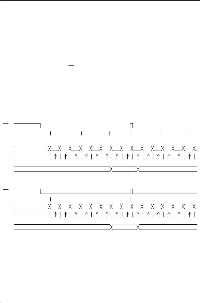
The relation between gray-scale data and data bus in the serial input is the same as that in the 8-bit parallel interface mode (described in the preceding section) at every gradation.
(1) 8-bit serial interface
When entering data (parameters): A0 = HIGH at the rising edge of the 8th SCL.
CS |
|
|
|
|
|
|
|
|
|
|
|
|
|
|
|
|
dot0(R) |
|
|
dot1(G) |
|
dot2(B) |
|
dot3(R) |
|
|
dot4(R) |
|
|
|
R2 |
R1 |
R0 |
G2 |
G1 |
G0 |
B1 |
B0 |
R2 |
R1 |
R0 |
G2 |
G1 |
G0 |
SI |
D7 |
D6 |
D5 |
D4 |
D3 |
D2 |
D1 |
D0 |
D7 |
D6 |
D5 |
D4 |
D3 |
D2 |
SCL |
|
|
|
|
|
|
|
|
|
|
|
|
|
|
|
1 |
2 |
3 |
4 |
5 |
6 |
7 |
8 |
1 |
2 |
3 |
4 |
5 |
6 |
A0 |
|
|
|
|
|
|
|
|
|
|
|
|
|
|
When entering command: A0 = LOW at the rising edge of the 8th SCL.
CS |
|
|
|
|
|
|
|
|
|
|
|
|
|
|
|
|
|
|
command |
|
|
|
|
|
command |
|
|
||
SI |
D7 |
D6 |
D5 |
D4 |
D3 |
D2 |
D1 |
D0 |
D7 |
D6 |
D5 |
D4 |
D3 |
D2 |
SCL |
|
|
|
|
|
|
|
|
|
|
|
|
|
|
|
1 |
2 |
3 |
4 |
5 |
6 |
7 |
8 |
1 |
2 |
3 |
4 |
5 |
6 |
A0 |
|
|
|
|
|
|
|
|
|
|
|
|
|
|
12 |
EPSON |
Rev. 1.0 |
S1D15G00 Series
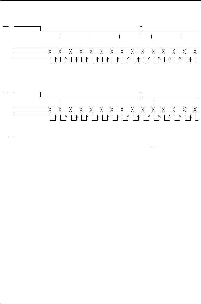
(2) 9-bit serial interface
When entering data (parameters): SI = HIGH at the rising edge of the 1st SCL.
CS |
|
|
|
|
|
|
|
|
|
|
|
|
|
|
|
|
|
dot0(R) |
|
|
dot1(G) |
|
dot2(B) |
|
dot3(R) |
|
|
||
|
|
R2 |
R1 |
R0 |
G2 |
G1 |
G0 |
B1 |
B0 |
|
R2 |
R1 |
R0 |
|
SI |
D/C |
D7 |
D6 |
D5 |
D4 |
D3 |
D2 |
D1 |
D0 |
D/C |
D7 |
D6 |
D5 |
D4 |
SCL |
|
|
|
|
|
|
|
|
|
|
|
|
|
|
|
1 |
2 |
3 |
4 |
5 |
6 |
7 |
8 |
9 |
1 |
2 |
3 |
4 |
5 |
When entering commands: SI = LOW at the rising edge of the 1st SCL.
CS |
|
|
|
|
|
|
|
|
|
|
|
|
|
|
|
|
|
|
command |
|
|
|
|
|
command |
|
|
||
SI |
D/C |
D7 |
D6 |
D5 |
D4 |
D3 |
D2 |
D1 |
D0 |
D/C |
D7 |
D6 |
D5 |
D4 |
SCL |
|
|
|
|
|
|
|
|
|
|
|
|
|
|
|
1 |
2 |
3 |
4 |
5 |
6 |
7 |
8 |
9 |
1 |
2 |
3 |
4 |
5 |
*If CS is caused to HIGH before 8 bits from D7 to D0 are entered, the data concerned is invalidated. Before entering succeeding sets of data, you must correctly input the data concerned again.
*In order to avoid data transfer error due to incoming noise, it is recommended to set CS at HIGH on byte basis to initialize the serial-to-parallel conversion counter and the register.
Rev. 1.0 |
EPSON |
13 |
S1D15G00 Series
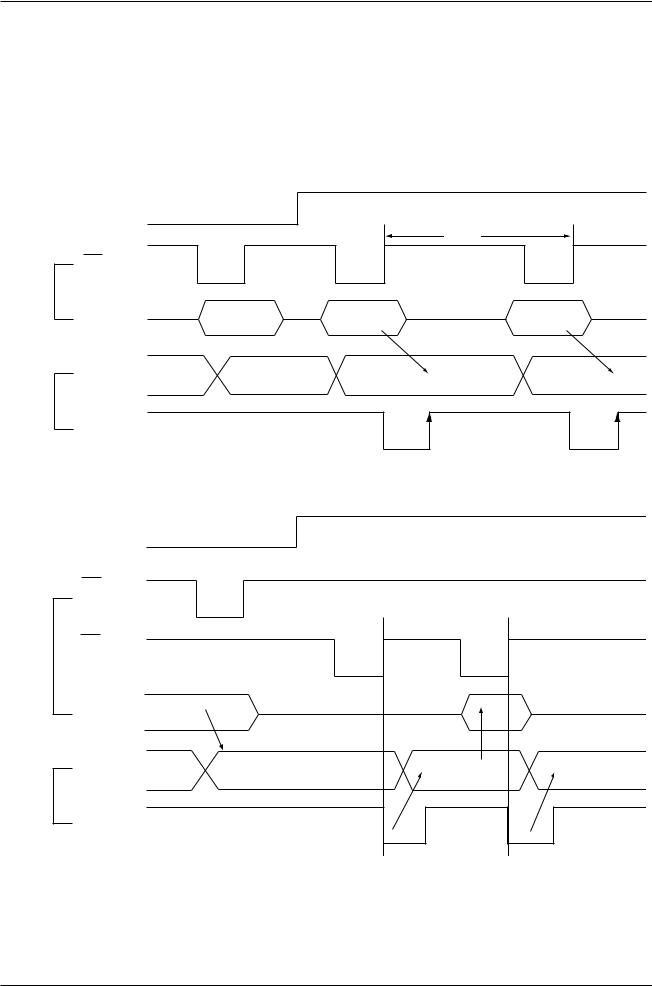
8.2 Access to DDRAM and Internal Registers
S1G15G00 realizes high-speed data transfer because the access from MPU is a sort of pipeline processing done via the bus holder attached to the internal, requiring the cycle time alone without needing the wait time.
For example, when MPU writes data to the DDRAM, the data is once held by the bus holder and then written to the DDRAM before the succeeding write cycle is started. When MPU reads data from the DDRAM, the first read cycle is dummy and the data read in the dummy cycle is held by the bus holder, and then it is read from the bus holder to the system bus in the succeeding read cycle. Fig. 8.2.1 illustrates these relations.
* Write operation
A0
tcyc
WR
MPU |
Command write |
Data write |
Data write |
DATA
Bus holder
Internal
Data write signal
* Read operation
A0 |
|
|
|
|
Command write |
|
|
WR |
|
|
|
|
Dummy read |
Data read |
|
RD |
|
|
|
MPU |
|
|
|
External pulse |
|
|
|
Bus holder |
Command |
RAM data |
RAM data |
Internal |
|
|
|
Data Read |
|
|
|
signal |
|
|
|
Fig. 8.2.1
*There is a restriction in the read sequence of the DDRAM. Namely, the data at the specified address is not output in the first data read conducted immediately after the memory read command (dummy read). It is read in the second data read.
14 |
EPSON |
Rev. 1.0 |
S1D15G00 Series
8.3 DDRAM
8.3.1 DDRAM
It is 396 × 168 × 4 bits capacity RAM prepared for storing dot data. You can access a desired bit by specifying the page address and column address.
Since display data from MPU - D7 to D0 and D1 to D8 - correspond to one or two pixels of RGB, data transfer-related restrictions are reduced, realizing the display flexibly.
The RAM on S1D15G00 is separated to a block per 4 line to allow the display system to process data on the block basis. MPU’s read and write operations to and from the RAM are performed via the I/O buffer circuit. Reading of the RAM for the liquid crystal drive is controlled from another separate circuit.
Refer to the following memory map for the RAM configuration.
1Models other than the S1D15G00D10*100 (models that have 132 RGB × 160 output) Memory Map (When using the 8 gray-scale. 8-bit mode)
|
|
|
|
RGB alignment (Command of data control parameter2=000) |
|
|
|
||||
|
|
|
|
|
|
|
|
Column |
|
|
|
LCD |
P11:0 |
|
|
0 |
|
|
1 |
|
|
131 |
|
read |
P11:1 |
|
|
131 |
|
|
132 |
|
|
0 |
|
direction |
|
|
|
|
|
|
|
||||
|
|
|
|
|
|
|
|
|
|
|
|
|
Color |
|
R |
G |
B |
R |
G |
B |
R |
G |
B |
|
Page |
Data |
D7 |
D4 |
D1 |
D7 |
D4 |
D1 |
D7 |
D4 |
D1 |
|
|
D6 |
D3 |
D0 |
D6 |
D3 |
D0 |
D6 |
D3 |
D0 |
|
|
P10:0 |
P10:1 |
|||||||||
Block |
D5 |
D2 |
|
D5 |
D2 |
|
D5 |
D2 |
|
||
|
|
|
|
|
|
||||||
0 |
0 |
167 |
|
|
|
|
|
|
|
|
|
|
1 |
166 |
|
|
|
|
|
|
|
|
|
|
2 |
165 |
|
|
|
|
|
|
|
|
|
|
3 |
164 |
|
|
|
|
|
|
|
|
|
1 |
4 |
163 |
|
|
|
|
|
|
|
|
|
|
5 |
162 |
|
|
|
|
|
|
|
|
|
|
6 |
161 |
|
|
|
|
|
|
|
|
|
|
7 |
160 |
|
|
|
|
|
|
|
|
|
2 |
8 |
159 |
|
|
|
|
|
|
|
|
|
|
9 |
158 |
|
|
|
|
|
|
|
|
|
40 |
160 |
7 |
|
|
|
|
|
|
|
|
|
|
161 |
6 |
|
|
|
|
|
|
|
|
|
|
162 |
5 |
|
|
|
|
|
|
|
|
|
|
163 |
4 |
|
|
|
|
|
|
|
|
|
41 |
164 |
3 |
|
|
|
|
|
|
|
|
|
|
|
|
|
|
|
|
|
|
|
||
|
165 |
2 |
|
|
|
|
|
|
|
|
|
|
166 |
1 |
|
|
|
|
|
|
|
|
|
|
167 |
0 |
|
|
|
|
|
|
|
|
|
SEGout |
|
|
1 |
2 |
3 |
4 |
5 |
6 |
394 |
395 |
396 |
Each of RGB data entered to D7 to D0 (3 or 2 bits) is converted to 4 bits before written to the RAM. You can change position of R and B with DATCTL command.
Rev. 1.0 |
EPSON |
15 |

S1D15G00 Series
Memory Map (When using the 8 gray-scale, 16-bit mode)
|
|
RGB alignment (Command of data control parameter2=000) |
|
|
|
||||||||||||
|
|
|
|
|
|
|
|
|
|
Column |
|
|
|
|
|
||
LCD |
P11: 0 |
|
|
0 |
|
|
0 |
|
|
1 |
|
|
1 |
|
|
65 |
|
read |
P11: 1 |
|
|
65 |
|
|
65 |
|
|
64 |
|
|
64 |
|
|
0 |
|
direction |
|
|
|
|
|
|
|
|
|
|
|
||||||
|
|
|
|
|
|
|
|
|
|
|
|
|
|
|
|
|
|
|
Color |
|
R |
G |
B |
R |
G |
B |
R |
G |
B |
R |
G |
B |
R |
G |
B |
|
|
Data |
D15 D12 D9 |
D7 |
D4 |
D1 D15 D12 D9 |
D7 |
D4 |
D1 |
D7 |
D4 |
D1 |
|||||
|
Page |
|
D14 D11 D8 |
D6 |
D3 |
D0 D14 D11 D8 |
D6 |
D3 |
D0 |
D6 |
D3 |
D0 |
|||||
|
|
|
|||||||||||||||
Block |
P10:0 |
P10:1 D13 D10 |
|
D5 |
D2 |
|
D13 D10 |
|
D5 |
D2 |
|
D5 |
D2 |
|
|||
0 |
0 |
167 |
|
|
|
|
|
|
|
|
|
|
|
|
|
|
|
|
1 |
166 |
|
|
|
|
|
|
|
|
|
|
|
|
|
|
|
|
2 |
165 |
|
|
|
|
|
|
|
|
|
|
|
|
|
|
|
|
3 |
164 |
|
|
|
|
|
|
|
|
|
|
|
|
|
|
|
1 |
4 |
163 |
|
|
|
|
|
|
|
|
|
|
|
|
|
|
|
|
5 |
162 |
|
|
|
|
|
|
|
|
|
|
|
|
|
|
|
|
6 |
161 |
|
|
|
|
|
|
|
|
|
|
|
|
|
|
|
|
7 |
160 |
|
|
|
|
|
|
|
|
|
|
|
|
|
|
|
2 |
8 |
159 |
|
|
|
|
|
|
|
|
|
|
|
|
|
|
|
|
9 |
158 |
|
|
|
|
|
|
|
|
|
|
|
|
|
|
|
40 |
160 |
7 |
|
|
|
|
|
|
|
|
|
|
|
|
|
|
|
|
161 |
6 |
|
|
|
|
|
|
|
|
|
|
|
|
|
|
|
|
162 |
5 |
|
|
|
|
|
|
|
|
|
|
|
|
|
|
|
|
163 |
4 |
|
|
|
|
|
|
|
|
|
|
|
|
|
|
|
41 |
164 |
3 |
|
|
|
|
|
|
|
|
|
|
|
|
|
|
|
|
|
|
|
|
|
|
|
|
|
|
|
|
|
|
|
||
|
165 |
2 |
|
|
|
|
|
|
|
|
|
|
|
|
|
|
|
|
166 |
1 |
|
|
|
|
|
|
|
|
|
|
|
|
|
|
|
|
167 |
0 |
|
|
|
|
|
|
|
|
|
|
|
|
|
|
|
SEGout |
|
|
1 |
2 |
3 |
4 |
5 |
6 |
7 |
8 |
9 |
10 |
11 |
12 |
394 395 396 |
||
Each of RGB data entered to D7 to D0 (3 or 2 bits) is converted to 4 bits before written to the RAM. You can change position of R and B with DATCTL command.
16 |
EPSON |
Rev. 1.0 |

S1D15G00 Series
Memory Map (When using the 16 gray-scale 8-bit mode)
RGB alignment (Command of data control parameter2=000)
|
|
|
|
|
|
|
|
|
|
Column |
|
|
|
|
|
||
LCD |
P11: 0 |
|
|
0 |
|
|
0 |
|
|
1 |
|
|
1 |
|
|
65 |
|
read |
P11: 1 |
|
|
65 |
|
|
65 |
|
|
64 |
|
|
64 |
|
|
0 |
|
direction |
|
|
|
|
|
|
|
|
|
|
|
||||||
|
|
|
|
|
|
|
|
|
|
|
|
|
|
|
|
|
|
|
Color |
|
R1 |
G1 B1 |
R2 G2 |
B2 |
R1 G1 |
B1 |
R |
G2 |
B2 |
R2 G2 |
B2 |
||||
|
|
Data |
D7 |
D3 |
D7 |
D3 |
D7 |
D3 |
D7 |
D3 |
D7 |
D3 D7 |
D3 |
D3 |
D7 |
D3 |
|
|
Page |
|
D6 |
D2 |
D6 |
D2 |
D6 |
D2 |
D6 |
D2 |
D6 |
D2 D6 |
D2 |
D2 |
D6 |
D2 |
|
Block |
P10:0 |
P10:1 |
D5 |
D1 |
D5 |
D1 |
D5 |
D1 |
D5 |
D1 |
D5 |
D1 |
D5 |
D1 |
D1 |
D5 |
D1 |
|
|
|
D4 |
D0 |
D4 |
D0 |
D4 |
D0 |
D4 |
D0 |
D4 |
D0 D4 |
D0 |
D0 |
D4 |
D0 |
|
0 |
0 |
167 |
|
|
|
|
|
|
|
|
|
|
|
|
|
|
|
|
1 |
166 |
|
|
|
|
|
|
|
|
|
|
|
|
|
|
|
|
2 |
165 |
|
|
|
|
|
|
|
|
|
|
|
|
|
|
|
|
3 |
164 |
|
|
|
|
|
|
|
|
|
|
|
|
|
|
|
1 |
4 |
163 |
|
|
|
|
|
|
|
|
|
|
|
|
|
|
|
|
5 |
162 |
|
|
|
|
|
|
|
|
|
|
|
|
|
|
|
|
6 |
161 |
|
|
|
|
|
|
|
|
|
|
|
|
|
|
|
|
7 |
160 |
|
|
|
|
|
|
|
|
|
|
|
|
|
|
|
2 |
8 |
159 |
|
|
|
|
|
|
|
|
|
|
|
|
|
|
|
|
9 |
158 |
|
|
|
|
|
|
|
|
|
|
|
|
|
|
|
40 |
160 |
7 |
|
|
|
|
|
|
|
|
|
|
|
|
|
|
|
|
161 |
6 |
|
|
|
|
|
|
|
|
|
|
|
|
|
|
|
|
162 |
5 |
|
|
|
|
|
|
|
|
|
|
|
|
|
|
|
|
163 |
4 |
|
|
|
|
|
|
|
|
|
|
|
|
|
|
|
41 |
164 |
3 |
|
|
|
|
|
|
|
|
|
|
|
|
|
|
|
|
|
|
|
|
|
|
|
|
|
|
|
|
|
|
|
||
|
165 |
2 |
|
|
|
|
|
|
|
|
|
|
|
|
|
|
|
|
166 |
1 |
|
|
|
|
|
|
|
|
|
|
|
|
|
|
|
|
167 |
0 |
|
|
|
|
|
|
|
|
|
|
|
|
|
|
|
SEGout |
|
|
1 |
2 |
3 |
4 |
5 |
6 |
7 |
8 |
9 |
10 |
11 |
12 |
394 395 396 |
||
You can change position of R and B with DATCTL command.
Rev. 1.0 |
EPSON |
17 |
Loading...