


SCI7654 |
PF754-03 |
SCI7654M0A/C0A
DC/DC Converter
 Double/Triple/Quadruple Boosting
 95% Excellent Power Conversion Efficiency
 Built-in Voltage Regulator
 DESCRIPTION
The SCI7654 is a highly efficient, but low power-consumption DC-to-DC converter based on the advanced CMOS technologies. It can generate an output voltage double/triple/quadruple times higher than the input (in negative direction) if 4/3/2 external capacitors are attached.
With a built-in voltage regulator, the SCI7654 can provide a stable output by setting the DC/DC output to any voltage via two external resistors. This is optimum to the LCD panel power supply as the stable output can have the negative temperature gradient required for an LCD panel.
 FEATURES
 An input voltage can be boosted double/triple/quadruple to negative potential.
 Input voltages: –2.4 to –5.5V (quadruple boosting), –2.4 to –7.3V (triple boosting), –2.4 to –11.0V (double boosting)
 Excellent vol tage conversion efficiency: 95% (Typ.)
 Large output current: 20 mA (Max.) during quadruple boosting
 Built-in voltage regulator (for stable voltage output)
 Built-in reference voltage source for accurate regulation: –1.5 ± 0.05V (CT0)
 Regulator output voltage temperature gradient function: –0.04, –0.15, –0.35, –0.55%/˚C
 Low current consumption: 130 A (Typ.)
 Low standby current: 5.0 A (Max.)
 Built-in oscillator circuit
 5/6-time voltage boosting in negative potential by serial connection
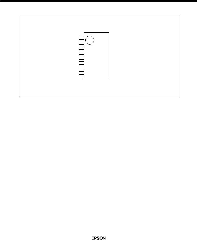
 Package: SCI7654M0A SSOP2-16pin (plastic), SCI7654C0A DIP-16pin (plastic)
 BLOCK DIAGRAM
VDD |
|
|
|
|
|
|
POFF1 |
Power-Off |
|
|
Ref. Voltage |
TC1 |
|
|
|
Circuit |
|
|||
|
Control |
|
|
TC2 |
||
POFF2 |
|
|
|
|||
|
|
|
|
|
|
|
FC |
Clock |
|
Booster Control |
RV |
||
Generator |
|
|
||||
|
|
|
Voltage Regulator |
VREG |
||
|
|
|
|
|
||
|
|
|
|
|
|
VRI |
VIN |
|
Voltage Converter |
|
VOUT |
||
|
C1P |
C1N |
C3N |
C2P |
C2N |
|
SCI7654M0A/C0A
 PIN CONFIGURATION
SSOP2-16pin/DIP-16pin
VOUT |
1 |
16 |
C2P |
VRI |
2 |
|
C2N |
15 |
|||
VREG |
3 |
|
C3N |
14 |
|||
RV |
4 |
|
C1N |
13 |
|||
VDD |
5 |
|
C1P |
12 |
|||
FC |
6 |
|
VIN |
11 |
|||
TC1 |
7 |
|
POFF1 |
10 |
|||
TC2 |
8 |
|
POFF2 |
9 |
 PIN DESCRIPTION
Pin No. |
Pin Name |
Function |
|
|
|
1 |
VOUT |
Voltage output |
|
|
|
2 |
VRI |
Regulator input |
|
|
|
3 |
VREG |
Regulator output |
|
|
|
4 |
RV |
Input for regulator output voltage adjustment |
|
|
|
5 |
VDD |
Input voltage pin (Positive) |
|
|
|
6 |
FC |
Internal clock rate switch input, and clock input in serial/parallel |
|
|
connection (Common input pin) |
|
|
|
7 |
TC1 |
Input for regulator output temperature gradient setup (1) |
|
|
|
8 |
TC2 |
Input for regulator output temperature gradient setup (2) |
|
|
|
9 |
POFF2 |
Power-off control input (2) |
|
|
|
10 |
POFF1 |
Power-off control input (1) |
|
|
|
11 |
VIN |
Input voltage pin (Negative) |
|
|
|
12 |
C1P |
Common double and quadruple boosting capacitor positive pin |
|
|
|
13 |
C1N |
Double boosting capacitor negative pin |
|
|
|
14 |
C3N |
Quadruple boosting capacitor negative pin |
|
|
|
15 |
C2N |
Triple boosting capacitor negative pin |
|
|
|
16 |
C2P |
Triple boosting capacitor positive pin |
|
|
|
2
SCI7654M0A/C0A
 ABSOLUTE MAXIMUM RATINGS
Rating |
Symbol |
|
Min. |
|
Max. |
Unit |
Remark |
Input Power Voltage |
VIN |
|
-26.0/N |
VDD +0.3 |
V |
N=Boosting time; |
|
|
|
|
|
|
|
|
at VIN pin |
|
|
|
|
|
|
|
|
Input Pin Voltage |
VI |
|
VIN -0.3 |
VDD +0.3 |
V |
POFF1, POFF2 |
|
|
|
|
|
|
|
|
TC1, TC2, FC pins |
|
|
|
|
|
|
|
|
Output Pin Voltage 1 |
V0C1 |
|
VIN -0.3 |
VDD +0.3 |
V |
At C1P and C2P pins |
|
|
|
|
|
|
|
|
|
Output Pin Voltage 2 |
VOC2 |
2 |
VIN -0.3 |
VIN +0.3 |
V |
At C1N pin |
|
|
|
|
|
|
|
|
|
Output Pin Voltage 3 |
VOC3 |
3 |
VIN -0.3 |
2 |
VIN +0.3 |
V |
At C2N pin |
|
|
|
|
|
|
|
|
Output Pin Voltage 4 |
VOC4 |
4 |
VIN -0.3 |
3 |
VIN +0.3 |
V |
At C3N pin |
|
|
|
|
|
|
|
|
Regulator Input Power Voltage |
VRI |
N |
VIN -0.3 |
VDD +0.3 |
V |
N=Boosting time; at VRI pin |
|
|
|
|
|
|
|
|
|
Regulator Input Pin Voltage |
VRV |
N |
VIN -0.3 |
VDD +0.3 |
V |
N=Boosting time; at RV pin |
|
|
|
|
|
|
|
|
|
Output Voltage |
V0 |
N |
VIN -0.3 |
VDD +0.3 |
V |
N=Boosting time; at VOUT |
|
|
|
|
|
|
|
|
and VREG pins |
|
|
|
|
|
|
|
|
Input Current |
IIN |
|
— |
|
80 |
mA |
At VIN pin |
|
|
|
|
|
|
|
|
Output Current |
IOUT |
|
— |
N≤ 4: |
20 |
mA |
N=Boosting time; at VOUT |
|
|
|
|
N>4: 80/N |
|
and VREG pins |
|
|
|
|
|
|
|
|
|
Allowable Loss |
Pd |
|
— |
|
210 |
mW |
— |
|
|
|
|
|
|
|
|
Operating Temperature |
Topr |
|
-30 |
|
85 |
˚C |
— |
|
|
|
|
|
|
|
|
Storage Temperature |
Tstg |
|
-55 |
|
150 |
˚C |
— |
|
|
|
|
|
|
|
|
Soldering Temperature and Time |
Tsol |
|
— |
|
260•10 |
˚C.S |
Temperature at leads |
 ELECTRICAL CHARACTERISTICS
(Unless otherwise designated: Ta=–30° V to +85° C, VDD=0V, VIN=–5.0V)
Characteristic |
Symbol |
Condition |
|
Min. |
Typ. |
Max. |
Unit |
|
|
|
|
|
|
|
|
Input Power Voltage 1 |
VIN1 |
During quadruple boosting |
-5.5 |
— |
-2.4 |
V |
|
|
|
|
|
|
|
|
|
Input Power Voltage 2 |
VIN2 |
During triple boosting |
|
-7.3 |
— |
-2.4 |
V |
|
|
|
|
|
|
|
|
Input Power Voltage 3 |
VIN3 |
During double boosting |
-11 |
|
-2.4 |
V |
|
|
|
|
|
|
|
|
|
Input Power Voltage N |
VINN |
During large-time boosting using |
-22/N |
— |
-2.4 |
V |
|
|
|
external diodes |
|
|
|
|
|
|
|
|
|
|
|
|
|
Boost Startup Input Power Voltage |
VSTA |
N=Boosting time, IOUT<200 A, |
-22/N |
— |
-2.4 |
V |
|
|
|
FC=VDD |
|
|
|
|
|
|
|
|
|
|
|
|
|
Booster Output Voltage |
VOUT |
— |
|
-22 |
— |
— |
V |
|
|
|
|
|
|
|
|
Regulator Input Voltage |
VRI |
— |
|
-22 |
— |
-2.4 |
V |
|
|
|
|
|
|
|
|
Regulator Output Voltage |
VREG |
IREG=0, VRI=-22V, |
|
— |
— |
-2.4 |
V |
|
|
|
|
|
|
|
|
|
|
RRV=1MΩ |
|
|
|
|
|
Booster Output Impedance |
ROUT |
IOUT=10mA, during quadruple |
— |
200 |
300 |
|
|
|
|
boosting |
|
|
|
|
|
|
|
|
|
|
|
|
|
Booster Power Conversion |
Peff |
IOUT=2 mA; during quadruple |
— |
95 |
— |
% |
|
Efficiency |
|
boosting; |
|
|
|
|
|
|
|
C1, C2, C3, COUT=10 |
F Tantalum |
|
|
|
|
|
|
|
|
|
|
|
|
Booster Operating Current |
IOPR1 |
FC=VDD, POFF1=VIN, POFF2=VDD; |
— |
130 |
220 |
A |
|
Consumption 1 |
|
during no loading; |
|
|
|
|
|
|
|
C1, C2, C3, COUT=10 |
F Tantalum |
|
|
|
|
|
|
|
|
|
|
|
|
Booster Operating Current |
IOPR2 |
FC=VIN, POFF1=VIN, POFF2=VDD; |
— |
520 |
880 |
A |
|
Consumption 2 |
|
during no loading; |
|
|
|
|
|
|
|
C1, C2, C3, COUT=10 |
F Tantalum |
|
|
|
|
|
|
|
|
|
|
|
|
Regulator Operating Current |
IOPVR |
VRI=-20 V, during no loading, |
— |
10 |
15 |
A |
|
Consumption |
|
RRV=1 M |
|
|
|
|
|
|
|
|
|
|
|
|
|
3
 Loading...