


MF1167-02 S1D13503F00A
LCD Controller ICs
S1D13305 Series
Technical Manual
No part of this material may be reproduced or duplicated in any form or by any means without the written permission of Seiko Epson. Seiko Epson reserves the right to make changes to this material without notice. Seiko Epson does not assume any liability of any kind arising out of any inaccuracies contained in this material or due to its application or use in any product or circuit and, further, there is no representation that this material is applicable to products requiring high level reliability, such as, medical products. Moreover, no license to any intellectual property rights is granted by implication or otherwise, and there is no representation or warranty that anything made in accordance with this material will be free from any patent or copyright infringement of a third party. This material or portions thereof may contain technology or the subject relating to strategic products under the control of the Foreign Exchange and Foreign Trade Law of Japan and may require an export license from the Ministry of International Trade and Industry or other approval from another government agency.
In this manual, Zilog's Z80-CPU or its equivalent shall be called Z80, Intel's 8085A or its equivalent shall be called 8085 and Motorola's MC6809 and MC6802 or their equivalents shall be called 6809 and 6802, respectively.
® stands for registered trade mark.
All other product names mentioned herein are trademarks and/or registered trademarks of their respec-
tive owners.
© Seiko Epson Corporation 2001 All rights reserved.
The information of the product number change
Starting April 1, 2001, the product number will be changed as listed below. To order from April 1, 2001 please use the new product number. For further information, please contact Epson sales representative.
Configuration of product number
 Devices
S1 |
|
D |
|
13706 |
|
F |
|
00A0 |
|
00 |
|
|
||||||
|
|
|
|
|
|
|
|
|
|
|
|
|
|
|
|
|
Packing specification |
|
|
|
|
|
|
|
|
|
|
|
|
|
|
|
|
|
|
||
|
|
|
|
|
|
|
|
|
|
|
|
|
|
|
|
|
Specification |
|
|
|
|
|
|
|
|
|
|
|
|
|
|
|
|
|
|
||
|
|
|
|
|
|
|
|
|
|
|
|
|
|
|
|
|
Package (B: CSP, F: QFP) |
|
|
|
|
|
|
|
|
|
|
|
|
|
|
|
|
|
|
||
|
|
|
|
|
|
|
|
|
|
|
|
|
|
|
|
|
Corresponding model number |
|
|
|
|
|
|
|
|
|
|
|
|
|
|
|
|
|
|
||
|
|
|
|
|
|
|
|
|
|
|
|
|
|
|
|
|
Model name (D: driver, digital products) |
|
|
|
|
|
|
|
|
|
|
|
|
|
|
|
|
|
|
||
|
|
|
|
|
|
|
|
|
|
|
|
|
|
|
|
|
Product classification (S1: semiconductor) |
|
|
|
|
|
|
|
|
|
|
|
|
|
|
|
|
|
|
||
 Evaluation Board
S5U 13705 P00C
Specification
Corresponding model number (13705: for S1D13705)
Product classification (S5U: development tool for semiconductor)
Comparison table between new and previous number
• S1D13305 Series |
• S1D1370x Series |
|
|
• S1D1380x Series |
||||
Previous No. |
New No. |
|
Previous No. |
|
New No. |
|
Previous No. |
New No. |
SED1335 Series |
S1D13305 Series |
|
SED137x Series |
|
S1D1370x Series |
|
SED138x Series |
S1D1380x Series |
SED1335D0A |
S1D13305D00A |
|
SED1374F0A |
|
S1D13704F00A |
|
SED1386F0A |
S1D13806F00A |
SED1335F0A |
S1D13305F00A |
|
SED1375F0A |
|
S1D13705F00A |
|
|
|
SED1335F0B |
S1D13305F00B |
|
|
|
|
|
||
|
|
|
|
|
|
|
||
|
|
|
SED1376B0A |
|
S1D13706B00A |
|
|
|
• S1D1350x Series |
|
|
|
|||||
|
SED1376F0A |
|
S1D13706F00A |
|
|
|
||
Previous No. |
New No. |
|
SED1378 Series |
|
S1D13708 Series |
|
|
|
SED135x Series |
S1D1350x Series |
|
|
|
|
|
|
|
|
• S1D13A0x Series |
|
|
|
||||
SED1353D0A |
S1D13503D00A |
|
|
|
|
|||
|
|
|
|
|
|
|
||
SED1353F0A |
S1D13503F00A |
|
Previous No. |
|
New No. |
|
|
|
SED1353F1A |
S1D13503F01A |
|
|
|
|
|
|
|
|
SED13Ax Series |
|
S1D13A0x Series |
|
|
|
||
SED1354F0A |
S1D13504F00A |
|
|
|
|
|
||
|
SED13A3F0A |
|
S1D13A03F00A |
|
|
|
||
SED1354F1A |
S1D13504F01A |
|
SED13A3B0B |
|
S1D13A03B00B |
|
|
|
SED1354F2A |
S1D13504F02A |
|
SED13A4B0B |
|
S1D13A04B00B |
|
|
|
SED1355F0A |
S1D13505F00A |
|
|
|
|
|
||
|
|
|
|
|
|
|
||
|
|
|
|
|
|
|
||
SED1356F0A |
S1D13506F00A |
|
|
|
|
|
|
|
|
|
|
|
|
|
|
|
|
Comparison table between new and previous number of Evaluation Boards
• S1D1350x Series |
|
• S1D1370x Series |
• S1D1380x Series |
|
||||
Previous No. |
New No. |
|
Previous No. |
New No. |
|
Previous No. |
|
New No. |
|
|
|
|
|
|
|
|
|
SDU1353#0C |
S5U13503P00C |
|
SDU1374#0C |
S5U13704P00C |
|
SDU1386#0C |
|
S5U13806P00C |
SDU1354#0C |
S5U13504P00C |
|
SDU1375#0C |
S5U13705P00C |
|
|
|
|
|
|
|
|
|
||||
SDU1355#0C |
S5U13505P00C |
|
SDU1376#0C |
S5U13706P00C |
|
|
|
|
SDU1356#0C |
S5U13506P00C |
|
SDU1376BVR |
S5U13706B32R |
|
|
|
|
|
|
|
|
|
|
|
||
|
|
|
SDU1378#0C |
S5U13708P00C |
|
|
|
|
|
|
|
|
|
|
|||
|
|
|
|
|
|
|
|
|
• S1D13A0x Series
Previous No. |
New No. |
SDU13A3#0C |
S5U13A03P00C |
SDU13A4#0C |
S5U13A04P00C |

|
|
|
|
|
CONTENTS |
|
|
|
|
|
CONTENTS |
1. |
OVERVIEW |
................................................................................................................................................................. |
|
1 |
|
2. |
FEATURES ................................................................................................................................................................. |
|
|
1 |
|
3. |
BLOCK DIAGRAM ....................................................................................................................................................... |
|
2 |
||
4. |
PINOUTS ..................................................................................................................................................................... |
|
|
3 |
|
5. |
PIN DESCRIPTION ..................................................................................................................................................... |
|
4 |
||
|
5.1. |
S1D13305F00A/00B ...................................................................................................................Pin Summary |
4 |
||
|
5.2. |
Pin Functions ..................................................................................................................................................... |
|
5 |
|
|
|
5.2.1. ......................................................................................................................................... |
Power supply |
5 |
|
|
|
5.2.2. ................................................................................................................................................ |
Oscillator |
|
5 |
|
|
5.2.3. ........................................................................................................................ |
Microprocessor interface |
5 |
|
|
|
5.2.4. ......................................................................................................................... |
Display memory control |
6 |
|
|
|
5.2.5. ................................................................................................................................... |
LCD drive signals |
7 |
|
6. |
SPECIFICATIONS ....................................................................................................................................................... |
|
7 |
||
|
6.1. |
Absolute ...............................................................................................................................Maximum Ratings |
7 |
||
|
6.2. |
S1D13305 .......................................................................................................................................................... |
|
8 |
|
|
6.3. |
S1D13305F ..........................................................................................................................Timing Diagrams |
10 |
||
|
|
6.3.1. .................................................................................................................8080 family interface timing |
10 |
||
|
|
6.3.2. .................................................................................................................6800 family interface timing |
11 |
||
|
|
6.3.3. ................................................................................................................Display memory read timing |
12 |
||
|
|
6.3.4. ................................................................................................................Display memory write timing |
13 |
||
|
|
6.3.5. .................................................................................................................SLEEP IN command timing |
15 |
||
|
|
6.3.6. ............................................................................................................External oscillator signal timing |
16 |
||
|
|
6.3.7. ................................................................................................................................ |
LCD output timing |
17 |
|
7. |
PACKAGE DIMENSIONS ......................................................................................................................................... |
19 |
|||
|
7.1. |
S1D13305F00A ............................................................................................................................................... |
|
19 |
|
|
7.2. |
S1D13305F00B ............................................................................................................................................... |
|
19 |
|
8. |
INSTRUCTION ..................................................................................................................................................SET |
|
20 |
||
|
8.1. |
The Command ...........................................................................................................................................Set |
20 |
||
|
8.2. |
System .............................................................................................................................Control Commands |
21 |
||
|
|
8.2.1. ...................................................................................................................................... |
SYSTEM SET |
21 |
|
|
|
........................................................................................................................................... |
8.2.1.1. |
C |
21 |
|
|
......................................................................................................................................... |
8.2.1.2. |
M0 |
21 |
|
|
......................................................................................................................................... |
8.2.1.3. |
M1 |
21 |
|
|
......................................................................................................................................... |
8.2.1.4. |
M2 |
22 |
|
|
....................................................................................................................................... |
8.2.1.5. |
W/S |
22 |
|
|
.......................................................................................................................................... |
8.2.1.6. |
IV |
23 |
|
|
......................................................................................................................................... |
8.2.1.7. |
FX |
24 |
|
|
........................................................................................................................................ |
8.2.1.8. |
WF |
25 |
|
|
......................................................................................................................................... |
8.2.1.9. |
FY |
25 |
|
|
....................................................................................................................................... |
8.2.1.10. C/R |
25 |
|
|
|
..................................................................................................................................... |
8.2.1.11. TC/R |
26 |
|
|
|
........................................................................................................................................ |
8.2.1.12. L/F |
26 |
|
|
|
......................................................................................................................................... |
8.2.1.13. AP |
27 |
|
|
|
8.2.2. ............................................................................................................................................. |
SLEEP IN |
27 |
|
|
8.3. |
Display .............................................................................................................................Control Commands |
28 |
||
|
|
8.3.1. ...................................................................................................................................... |
DISP ON/OFF |
28 |
|
|
|
........................................................................................................................................... |
8.3.1.1. |
D |
28 |
|
|
......................................................................................................................................... |
8.3.1.2. |
FC |
28 |
|
|
......................................................................................................................................... |
8.3.1.3. |
FP |
28 |
|
|
8.3.2. ............................................................................................................................................... |
SCROLL |
|
29 |
|
|
........................................................................................................................................... |
8.3.2.1. |
C |
29 |
|
|
............................................................................................................................... |
8.3.2.2. |
SL1, SL2 |
30 |
S1D13305 Series
Technical Manual
EPSON |
i |

CONTENTS
|
8.3.3. |
CSRFORM ........................................................................................................................................... |
34 |
|
|
|
8.3.3.1. |
CRX ...................................................................................................................................... |
34 |
|
|
8.3.3.2. |
CRY ...................................................................................................................................... |
34 |
|
|
8.3.3.3. |
CM ........................................................................................................................................ |
34 |
|
8.3.4. |
CSRDIR ............................................................................................................................................... |
|
34 |
|
8.3.5. |
OVLAY ................................................................................................................................................. |
|
35 |
|
|
8.3.5.1. |
MX0, MX1 ............................................................................................................................. |
35 |
|
|
8.3.5.2. |
DM1, DM2 ............................................................................................................................ |
36 |
|
|
8.3.5.3. |
OV ........................................................................................................................................ |
36 |
|
8.3.6. CGRAM ADR ....................................................................................................................................... |
36 |
||
|
8.3.7. |
HDOT SCR .......................................................................................................................................... |
37 |
|
|
|
8.3.7.1. |
D0 to D2 ............................................................................................................................... |
37 |
8.4. |
Drawing Control Commands ............................................................................................................................ |
37 |
||
|
8.4.1. |
CSRW .................................................................................................................................................. |
|
37 |
|
8.4.2. |
CSRR ................................................................................................................................................... |
|
38 |
8.5. |
Memory Control Commands ............................................................................................................................ |
38 |
||
|
8.5.1. |
MWRITE |
.............................................................................................................................................. |
38 |
|
8.5.2 |
MREAD ................................................................................................................................................ |
|
39 |
9. DISPLAY CONTROL FUNCTIONS ........................................................................................................................... |
40 |
|||
9.1. |
Character Configuration ................................................................................................................................... |
40 |
||
9.2. |
Screen Configuration ....................................................................................................................................... |
42 |
||
|
9.2.1. |
Screen configuration ............................................................................................................................ |
42 |
|
|
9.2.2. |
Display address scanning .................................................................................................................... |
42 |
|
|
9.2.3. |
Display scan timing .............................................................................................................................. |
45 |
|
9.3. |
Cursor Control .................................................................................................................................................. |
|
46 |
|
|
9.3.1. |
Cursor register function ........................................................................................................................ |
46 |
|
|
9.3.2. |
Cursor movement ................................................................................................................................ |
46 |
|
|
9.3.3. |
Cursor display layers ........................................................................................................................... |
46 |
|
9.4. Memory to Display Relationship ...................................................................................................................... |
48 |
|||
9.5. |
Scrolling ........................................................................................................................................................... |
|
51 |
|
|
9.5.1. |
On-page scrolling ................................................................................................................................. |
51 |
|
|
9.5.2. |
Inter-page scrolling .............................................................................................................................. |
51 |
|
|
9.5.3. |
Horizontal scrolling ............................................................................................................................... |
52 |
|
|
9.5.4. |
Bidirectional scrolling ........................................................................................................................... |
53 |
|
|
9.5.5. |
Scroll units ........................................................................................................................................... |
53 |
|
10. CHARACTER GENERATOR .................................................................................................................................... |
54 |
|||
10.1. CG Characteristics ........................................................................................................................................... |
54 |
|||
|
10.1.1. Internal character generator ................................................................................................................. |
54 |
||
|
10.1.2. External character generator ROM ...................................................................................................... |
54 |
||
|
10.1.3. Character generator RAM .................................................................................................................... |
54 |
||
10.2. CG Memory Allocation ..................................................................................................................................... |
55 |
|||
10.3. Setting the Character Generator Address ........................................................................................................ |
56 |
|||
|
10.3.1. |
M1 = 1 .................................................................................................................................................. |
|
56 |
|
10.3.2. CG RAM addressing example ............................................................................................................. |
57 |
||
10.4. Character Codes |
.............................................................................................................................................. |
58 |
||
11. MICROPROCESSOR INTERFACE .......................................................................................................................... |
59 |
|||
11.1. System Bus Interface ....................................................................................................................................... |
59 |
|||
|
11.1.1. |
8080 series .......................................................................................................................................... |
59 |
|
|
11.1.2. |
6800 series .......................................................................................................................................... |
59 |
|
11.2. Microprocessor Synchronization ...................................................................................................................... |
59 |
|||
|
11.2.1. Display status indication output ........................................................................................................... |
59 |
||
|
11.2.2. Internal register access ........................................................................................................................ |
59 |
||
|
11.2.3. Display memory access ....................................................................................................................... |
59 |
||
11.3. Interface Examples .......................................................................................................................................... |
61 |
|||
|
11.3.1. |
Z80 to S1D13305 series interface ....................................................................................................... |
61 |
|
|
11.3.2. |
6802 to S1D13305 series interface ...................................................................................................... |
61 |
|
ii |
EPSON |
S1D13305 Series
Technical Manual

|
|
CONTENTS |
12. |
DISPLAY MEMORY INTERFACE ............................................................................................................................. |
62 |
|
12.1. Static RAM ....................................................................................................................................................... |
62 |
|
12.2. Supply Current during Display Memory Access ............................................................................................... |
63 |
13. |
OSCILLATOR CIRCUIT ............................................................................................................................................ |
63 |
14. |
STATUS FLAG .......................................................................................................................................................... |
63 |
15. |
RESET ....................................................................................................................................................................... |
65 |
16. |
APPLICATION NOTES ............................................................................................................................................. |
65 |
|
16.1. Initialization Parameters ................................................................................................................................... |
65 |
|
16.1.1. SYSTEM SET instruction and parameters ........................................................................................... |
65 |
|
16.1.2. Initialization example ............................................................................................................................ |
66 |
|
16.1.3. Display mode setting example 1: combining text and graphics .......................................................... |
72 |
|
16.1.4. Display mode setting example 2: combining graphics and graphics .................................................. |
73 |
|
16.1.5. Display mode setting example 3: combining three graphics layers .................................................... |
75 |
|
16.2. System Overview ............................................................................................................................................. |
76 |
|
16.3 System Interconnection ................................................................................................................................... |
77 |
|
16.3.1. S1D13305F .......................................................................................................................................... |
77 |
|
16.4. Smooth Horizontal Scrolling ............................................................................................................................. |
79 |
|
16.5. Layered Display Attributes ............................................................................................................................... |
80 |
|
16.5.1. Inverse display ..................................................................................................................................... |
80 |
|
16.5.2. Half-tone display .................................................................................................................................. |
80 |
|
16.5.2.1. Menu pad display ................................................................................................................. |
80 |
|
16.5.2.2. Graph display ....................................................................................................................... |
81 |
|
16.5.3. Flashing areas ..................................................................................................................................... |
81 |
|
16.5.3.1. Small area ............................................................................................................................ |
81 |
|
16.5.3.2. Large area ............................................................................................................................ |
81 |
|
16.6. 16 × 16-dot Graphic Display ............................................................................................................................. |
81 |
|
16.6.1. Command usage .................................................................................................................................. |
81 |
|
16.6.2. Kanji character display ......................................................................................................................... |
81 |
17. |
INTERNAL CHARACTER GENERATOR FONT ....................................................................................................... |
84 |
18. |
GLOSSARY OF TERMS ........................................................................................................................................... |
85 |
Request for Information on S1D13305 Series ................................................................................................................. |
86 |
|
S1D13305 Series
Technical Manual
EPSON |
iii |

OVERVIEW/FEATURES
1. OVERVIEW
The S1D13305 series is a controller IC that can display text and graphics on LCD panel.
The S1D13305 series can display layered text and graphics, scroll the display in any direction and partition the display into multiple screens.
The S1D13305 series stores text, character codes and bitmapped graphics data in external frame buffer memory. Display controller functions include transferring data from the controlling microprocessor to the buffer memory, reading memory data, converting data to display pixels and generating timing signals for the buffer memory, LCD panel.
The S1D13305 series has an internal character generator with 160, 5 × 7 pixel characters in internal mask ROM. The character generators support up to 64, 8 × 16 pixel characters in external character generator RAM and up to 256, 8 × 16 pixel characters in external character generator ROM.
2. FEATURES
• Text, graphics and combined text/graphics display modes
• Three overlapping screens in graphics mode
• Up to 640 × 256 pixel LCD panel display resolution
• Programmable cursor control
• Smooth horizontal and vertical scrolling of all or part of the display
• 1/2-duty to 1/256-duty LCD drive
• Up to 640 × 256 pixel LCD panel display resolution memory
• 160, 5× 7 pixel characters in internal mask-program- med character generator ROM
• Up to 64, 8× 16 pixel characters in external character generator RAM
• Up to 256, 8× 16 pixel characters in external character generator ROM
• 6800 and 8080 family microprocessor interfaces
• Low power consumption—3.5 mA operating current (VDD = 3.5V), 0.05 μA standby current
• |
Package |
|
|
|
|
|
line-up |
Package |
|
|
|
|
S1D13305F00A |
QFP5-60 pin |
|
|
|
|
S1D13305F00B |
QFP6-60 pin |
|
|
|
• |
2.7 to 5.5 V (S1D13305F) |
|
S1D13305 Series
Technical Manual
EPSON |
1 |
BLOCK DIAGRAM
3. BLOCK DIAGRAM
|
Video RAM |
|
|
|
Character |
|
|
|
|
|
|
|
|
|
|
|
|
LCD |
|
||
|
|
Character |
|
|
Generator ROM |
|
|
|||
|
|
|
|
|
|
|
|
|||
|
|
Generator RAM |
|
|
|
|
|
|
|
|
VA0 to VA15 |
VCE |
VRD, VWR (S1D13305F) |
|
VD0 to VD7 |
YSCL, YD, YDIS |
LP, WF |
XSCL |
XD0 to XD3 |
||
|
|
|
|
|||||||
|
Video RAM Interface |
|
|
Input/Output |
LCD Controller |
|
||||
|
|
|
Register |
|
||||||
|
|
|
|
|
|
|
|
|
|
|
Cursor |
|
Display |
|
|
Refresh |
|
Character |
|
Layered |
|
Address |
|
Address |
|
|
Dot Counter |
Generator |
|
|
||
|
|
|
Counter |
Controller |
||||||
Controller |
|
Controller |
|
|
|
ROM |
||||
|
|
|
|
|
|
|
|
|||
|
|
Microprocessor Interface |
|
|
|
Oscillator |
||||
|
|
SEL0 SEL1 |
RES |
RD, WR |
A0, CS |
D0 to D7 |
|
XG |
|
XD |
|
|
|
|
|
|
|||||
2 |
EPSON |
S1D13305 Series
Technical Manual

PINOUTS
4. PINOUTS
àS1D13305F00A |
|
|
|
|
|
|
|
|
|
|
|
|
|
|
|
|
|
|
|
|
|
|
|
|
|
|
|
|
|
|
|
àS1D13305F00B |
|
|
|
|
|
|
|
|
|
|
|
|
|
|
|
|
|
|
|
|
|
|
|
|
|
|
|
|
|
|
|
|
|
|
|
||||||||||||||
|
|
XG SEL1 |
SEL2 |
|
WR |
|
|
|
|
VRD |
|
VCE |
|
VWR |
VA0 |
VA1 |
VA2 |
VA3 |
VA4 |
VA5 |
VA6 |
VA7 |
|
|
|
|
|
VD4 |
VD5 |
VD6 |
VD7 YSCL YD |
|
YDIS WF LP VSS |
XSCL XECL XD0 |
XD1 |
|
XD2 |
|
|
||||||||||||||||||||||||||||||||||||||||||
|
|
|
|
RD |
NC |
NC |
RES |
|
|
|
|
|
|
|
|
|
|
|
|||||||||||||||||||||||||||||||||||||||||||||||||||||||||||||||
|
|
|
|
|
|
|
|
|
|
|
|
|
|
|
|||||||||||||||||||||||||||||||||||||||||||||||||||||||||||||||||||
|
|
|
|
|
|
|
|
|
|
|
|
|
|
|
|
|
|
|
|
|
|
|
|
|
|
|
|
|
|
|
|
|
|
|
|
|
|
|
|
|
|
|
|
|
|
|
|
|
|
|
|
|
|
|
|
|
|
|
|
|
|
|
|
|
|
|
|
|
|
|
|
|
|
|
|
|
|
|
|
|
|
|
|
|
|
|
|
|
|
|
|
|
|
|
|
|
|
|
|
|
|
|
|
|
|
|
|
|
|
|
|
|
|
|
|
|
|
|
|
|
|
|
|
|
|
|
|
|
|
|
|
|
|
|
|
|
|
|
|
|
|
|
|
|
|
|
|
|
|
|
|
|
|
|
|
|
|
|
|
|
|
|
|
|
|
|
|
|
|
|
|
|
|
|
|
|
|
|
|
|
|
|
|
|
|
|
|
|
|
|
|
|
|
|
|
|
|
|
|
|
|
|
|
|
|
|
|
VD3 |
|
|
45 |
|
|
|
|
|
|
|
|
|
|
|
|
|
|
|
|
|
|
|
|
|
|
|
|
|
|
|
31 |
|
XD3 |
||||
|
|
|
|
|
|
|
|
|
|
|
|
|
|
|
|
|
|
|
|
|
|
|
|
|
|
|
|
|
|
|
|
|
|
|
|
|
|
|
|
|
|
|
|
VD2 |
|
|
46 |
|
|
|
|
|
|
|
|
|
|
|
|
|
|
|
|
|
|
|
|
|
|
|
|
|
|
|
|
30 |
|
D7 |
|||
XD |
|
|
|
|
|
|
|
|
|
50 |
|
|
|
|
|
|
|
45 |
|
|
|
|
|
|
|
40 |
|
|
|
|
|
|
|
|
|
VA8 |
VD1 |
|
|
|
|
|
|
|
|
|
|
|
|
|
|
|
|
|
|
|
|
|
|
|
|
|
|
|
|
|
|
|
|
|
|
|
|
D6 |
|||||||
CS |
|
|
|
|
|
|
|
|
|
|
|
|
|
|
|
|
|
|
|
|
|
|
|
|
|
|
|
|
|
|
|
|
|
|
|
|
|
|
|
|
|
|
VA9 |
VD0 |
|
|
|
|
|
|
|
|
|
|
|
|
|
|
|
|
|
|
|
|
|
|
|
|
|
|
|
|
|
|
|
|
|
|
|
|
D5 |
A0 |
|
|
|
|
|
|
|
|
|
|
|
|
|
|
|
|
|
|
|
|
|
|
|
|
|
|
|
|
|
|
|
|
|
|
|
|
|
|
|
|
|
|
VA10 |
VA15 |
|
|
|
|
|
|
|
|
|
|
|
|
|
|
|
|
|
|
|
|
|
|
|
|
|
|
|
|
|
|
|
|
|
|
|
|
D4 |
VDD |
|
|
|
|
|
|
|
|
|
|
|
|
|
|
|
|
|
|
|
|
|
|
|
|
|
|
|
|
|
|
|
|
|
|
|
|
|
|
|
|
|
|
VA11 |
VA14 |
|
|
|
|
|
|
|
|
|
|
|
|
|
|
|
|
|
|
|
|
|
|
|
|
|
|
|
|
|
|
|
|
|
|
|
|
D3 |
D0 |
|
60 |
|
|
|
|
|
|
|
|
|
S1D13305F00A |
|
|
|
|
|
|
30 |
|
VA12 |
VA13 |
|
|
|
|
|
|
|
|
|
S1D13305F00B |
|
|
|
|
|
D2 |
|||||||||||||||||||||||||||||||||||||||||||
D1 |
|
|
|
|
|
|
|
|
|
|
|
|
|
|
|
|
|
VA13 |
VA12 |
|
|
|
|
|
|
|
|
|
|
|
|
|
|
D1 |
|||||||||||||||||||||||||||||||||||||||||||||||
|
|
|
|
|
|
|
|
|
|
|
|
|
|
|
|
|
|
|
|
|
|
|
|
|
|
|
|
|
|||||||||||||||||||||||||||||||||||||||||||||||||||||
D2 |
|
1 |
|
|
|
|
|
Index |
|
|
|
|
|
|
|
|
|
|
|
|
|
|
|
|
|
|
|
|
|
|
|
29 |
|
NC |
VA11 |
|
|
|
|
|
|
|
|
|
|
Index |
|
|
|
|
|
|
|
|
|
|
|
|
|
|
|
|
|
|
|
|
|
|
D0 |
||||||||||||
|
|
|
|
|
|
|
|
|
|
|
|
|
|
|
|
|
|
|
|
|
|
|
|
|
|
|
|
|
|
|
|
|
|
|
|
|
|
|
|
|
|
|
|
|
|
|
|
|
|
|
|
|
|
|
|
|
|
|
|
|
|
|
|
|
|
|
|
|
|||||||||||||
D3 |
|
|
|
|
|
|
|
|
|
|
|
|
|
|
|
|
|
|
|
|
|
|
|
|
|
|
|
|
|
|
|
|
|
|
|
|
|
|
|
|
|
|
VA14 |
VA10 |
|
|
|
|
|
|
|
|
|
|
|
|
|
|
|
|
|
|
|
|
|
|
|
|
|
|
|
|
|
|
|
|
|
|
|
|
VDD |
D4 |
|
|
|
|
|
|
|
|
|
|
|
|
|
|
|
|
|
|
|
|
|
|
|
|
|
|
|
|
|
|
|
|
|
|
|
|
|
|
|
|
|
|
VA15 |
VA9 |
|
|
|
|
|
|
|
|
|
|
|
|
|
|
|
|
|
|
|
|
|
|
|
|
|
|
|
|
|
|
|
|
|
|
|
|
A0 |
D5 |
|
|
|
|
|
|
|
|
|
|
|
|
|
|
|
|
|
|
|
|
|
|
|
|
|
|
|
|
|
|
|
|
|
|
|
|
|
|
|
|
|
|
VD0 |
VA8 |
|
|
|
|
|
|
|
|
|
|
|
|
|
|
|
|
|
|
|
|
|
|
|
|
|
|
|
|
|
|
|
|
|
|
|
|
CS |
D6 |
|
|
|
|
|
|
|
|
|
|
|
|
|
|
|
|
|
|
|
|
|
|
|
|
|
|
|
|
|
|
|
|
|
|
|
|
|
|
|
|
|
|
VD1 |
|
|
|
|
|
|
|
|
|
|
|
|
|
|
|
|
|
|
|
|
|
|
|
|
|
|
|
|
|
|
|
|
|
|
|
|
|
|
|
5 6 |
|
|
|
|
|
|
|
10 |
|
|
|
|
|
15 |
|
|
|
|
|
|
|
20 |
|
|
|
|
|
|
|
VD2 |
VA7 |
|
|
|
|
|
|
|
|
|
|
|
|
|
|
|
|
|
|
|
|
|
|
|
|
|
|
|
|
|
|
|
|
|
|
|
|
XD |
||||||||||||
|
|
|
|
|
|
|
|
|
|
|
|
|
|
|
|
|
|
|
|
|
|
|
|
|
|
|
VA6 |
|
|
60 |
|
|
|
|
|
|
|
|
|
|
|
|
|
|
|
|
|
|
|
|
|
|
|
|
|
|
|
|
16 |
|
XG |
||||||||||||||||||||
|
|
|
|
|
|
|
|
|
|
|
|
|
|
|
|
|
|
|
|
|
|
|
|
|
|
|
|
|
|
|
|
|
|
|
|
|
|
|
|
|
|
|
|
NC |
|
|
|
|
|
|
|
|
|
|
|
|
|
|
|
|
|
|
|
|
|
|
|
|
|
|
|
|
|
|
|
SEL1 |
|||||
|
|
|
|
|
|
|
|
|
|
|
|
|
|
|
|
|
|
|
|
|
|
|
|
|
|
|
|
|
|
|
|
|
|
|
|
|
|
|
|
|
|
|
|
|
|
|
1 |
|
|
|
|
|
|
|
|
|
|
|
|
|
|
|
|
|
|
|
|
|
|
|
|
|
|
|
|
15 |
|
|
|||
|
|
|
|
|
|
|
|
|
|
|
|
|
|
|
|
|
|
|
|
|
|
|
|
|
|
|
|
|
|
|
|
|
|
|
|
|
|
|
|
|
|
|
|
|
|
|
|
|
|
|
|
|
|
|
|
|
|
|
|
|
|
|
|
|
|
|
|
||||||||||||||
|
|
|
|
|
|
|
|
|
|
|
|
|
|
|
|
|
|
|
|
|
|
|
|
|
|
|
|
|
|
|
|
|
|
|
|
|
|
|
|
|
|
|
|
|
|
|
|
|
|
|
|
|
|
|
|
|
|
|
|
|
|
|
|
|
|
|
|
|
|
|
|
|
|
|
|
|
|
|
|
|
|
|
|
|
|
D7 |
XD3 |
|
XD2 |
|
XD1 |
XD0 |
XECL XSCL VSS |
|
LP |
WF |
YDIS |
YD |
YSCL |
VD7 |
VD6 |
VD5 |
VD4 |
VD3 |
|
|
|
|
|
|
|
|
|
|
|
|
|
|
|
|
|
|
|
|
|
|
|
|
|
|
|
|
|
|
|
|
|
|
|
|
|
|
|
|
|||||||||||||||||||
|
|
|
|
|
|
|
|
|
|
|
|
VA5 |
VA4 |
VA3 |
VA2 VA1 VA0 |
|
VWR |
|
VCE |
|
VRD |
|
RES |
NC NC |
|
RD |
|
WR |
|
SEL 2 |
|
|
|||||||||||||||||||||||||||||||||||||||||||||||||
|
|
|
|
|
|
|
|
|
|
|
|
|
|
|
|||||||||||||||||||||||||||||||||||||||||||||||||||||||||||||||||||
|
|
|
|
|
|
|
|
|
|
|
|
|
|
|
|
|
|
|
|
|
|
|
|
|
|
|
|
|
|
|
|
|
|
|
|
|
|
|
|
|
|
|
|||||||||||||||||||||||||||||||||||||||
|
|
|
|
|
|
|
|
|
|
|
|
|
|
|
|
|
|
|
|
|
|
|
|
|
|
|
|
|
|
|
|
|
|
|
|
|
|
|
|
|
|
|
|
|
|
|
|
|
|
||||||||||||||||||||||||||||||||
|
|
|
|
|
|
|
|
|
|
|
|
|
|
|
|
|
|
|
|
|
|
|
|
|
|
|
|
|
|
|
|
|
|
|
|
|
|
|
|
|
|
|
|
|
|
|
|
|
|
|
|
|
|
|
|
|
|
|
|
|
|
|
|
|
|
|
|
|
|
|
|
|
|
||||||||
|
|
|
|
|
|
|
|
|
|
|
|
|
|
|
|
|
|
|
|
|
|
|
|
|
|
|
|
|
|
|
|
|
|
|
|
|
|
|
|
|
|
|
|
|
|
|
|
|
|
|
|
|
|
|
|
|
|
|
|
|
|
|
|
|
|
|
|
|
|
|
|
|
|
|
|
|
|
|
|
||
S1D13305 Series
Technical Manual
EPSON |
3 |

PIN DESCRIPTION
5.PIN DESCRIPTION
5.1. S1D13305F00A/00B Pin Summary
|
|
|
|
Name |
Number |
Type |
Description |
||||||||
|
|
|
|
S1D13305F00A |
S1D13305F00B |
||||||||||
|
|
|
|
|
|
|
|
|
|
|
|
|
|||
VA0 to VA15 |
27 to 28 |
1 to 6 |
Output |
VRAM address bus |
|||||||||||
30 to 43 |
50 to 59 |
||||||||||||||
|
|
|
|
|
|
|
|
|
|
|
|
|
|||
|
|
|
|
|
|
|
|
|
|
|
|
|
|
|
|
|
|
|
|
|
|
|
|
|
44 |
7 |
Output |
VRAM write signal |
|||
VWR |
|||||||||||||||
|
|
|
|
|
|
|
|
45 |
8 |
Output |
Memory control signal |
||||
VCE |
|||||||||||||||
|
|
|
|
|
|
|
46 |
9 |
Output |
VRAM read signal |
|||||
VRD |
|||||||||||||||
|
|
|
|
|
|
47 |
10 |
Input |
Reset |
||||||
RES |
|||||||||||||||
NC |
28, 48, 49 |
11, 12, 60 |
— |
No connection |
|||||||||||
|
|
|
|
|
|
|
|
|
|
|
|
|
|
|
|
|
|
|
|
|
|
|
|
|
|
|
|
8080 family: Read signal |
|||
RD |
50 |
13 |
Input |
||||||||||||
6800 family: Enable clock (E) |
|||||||||||||||
|
|
|
|
|
|
|
|
|
|
|
|
||||
|
|
|
|
|
|
|
|
|
|
|
|
|
|
|
|
|
|
|
|
|
|
|
|
|
|
|
|
8080 family: Write signal |
|||
WR |
51 |
14 |
Input |
||||||||||||
|
|
|
|||||||||||||
6800 family: R/W signal |
|||||||||||||||
|
|
|
|
|
|
|
|
|
|
|
|
||||
SEL2 |
52 |
15 |
Input |
8080 or 6800 family interface |
|||||||||||
select |
|||||||||||||||
|
|
|
|
|
|
|
|
|
|
|
|
||||
SEL1 |
53 |
16 |
Input |
8080 or 6800 family interface |
|||||||||||
select |
|||||||||||||||
|
|
|
|
|
|
|
|
|
|
|
|
||||
XG |
54 |
17 |
Input |
Oscillator connection |
|||||||||||
|
|
|
|
|
|
|
|
|
|
|
|
|
|
|
|
XD |
55 |
18 |
Output |
Oscillator connection |
|||||||||||
|
|
|
|
|
|
|
|
|
|
|
|
|
|
|
|
|
|
|
56 |
19 |
Input |
Chip select |
|||||||||
CS |
|||||||||||||||
A0 |
57 |
20 |
Input |
Data type select |
|||||||||||
|
|
|
|
|
|
|
|
|
|
|
|
|
|
|
|
VDD |
58 |
21 |
Supply |
2.7 to 5.5V supply |
|||||||||||
D0 to D7 |
59 to 60 |
22 to 29 |
Input/output |
Data bus |
|||||||||||
1 to 6 |
|||||||||||||||
|
|
|
|
|
|
|
|
|
|
|
|
|
|
||
|
|
|
|
|
|
|
|
|
|
|
|
|
|
|
|
XD0 to XD3 |
7 to 10 |
30 to 33 |
Output |
X-driver data |
|||||||||||
|
|
|
|
|
|
|
|
|
|
|
|
|
|
|
|
XECL |
11 |
34 |
Output |
X-driver enable chain clock |
|||||||||||
|
|
|
|
|
|
|
|
|
|
|
|
|
|
|
|
XSCL |
12 |
35 |
Output |
X-driver data shift clock |
|||||||||||
|
|
|
|
|
|
|
|
|
|
|
|
|
|
|
|
VSS |
13 |
36 |
Supply |
Ground |
|||||||||||
LP |
14 |
37 |
Output |
Latch pulse |
|||||||||||
|
|
|
|
|
|
|
|
|
|
|
|
|
|
|
|
WF |
15 |
38 |
Output |
Frame signal |
|||||||||||
|
|
|
|
|
|
|
|
|
|
|
|
|
|
|
|
YDIS |
16 |
39 |
Output |
Power-down signal when display is |
|||||||||||
blanked |
|||||||||||||||
|
|
|
|
|
|
|
|
|
|
|
|
||||
|
|
|
|
|
|
|
|
|
|
|
|
|
|
|
|
YD |
17 |
40 |
Output |
Scan start pulse |
|||||||||||
|
|
|
|
|
|
|
|
|
|
|
|
|
|
|
|
YSCL |
18 |
41 |
Output |
Y-driver shift clock |
|||||||||||
|
|
|
|
|
|
|
|
|
|
|
|
|
|
|
|
VD0 to VD7 |
19 to 26 |
42 to 49 |
Input/output |
VRAM data bus |
|||||||||||
|
|
|
|
|
|
|
|
|
|
|
|
|
|
|
|
4 |
EPSON |
S1D13305 Series
Technical Manual
PIN DESCRIPTION
5.2. |
Pin Functions |
||
5.2.1. |
Power supply |
||
|
|
||
Pin Name |
Function |
||
VDD |
2.7 to 5.5V supply. |
||
This may be the same supply as the controlling microprocessor. |
|||
|
|
||
|
|
||
VSS |
Ground |
||
Note: The peak supply current drawn by the S1D13305 series may be up to ten times the average supply current. The power
supply impedance must be kept as low as possible by ensuring that supply lines are sufficiently wide and by placing 0.47 μF decoupling capacitors that have good high-frequency response near the device’s supply pins.
5.2.2. Oscillator
Pin Name |
Function |
|
|
|
|
XG |
Crystal connection for internal oscillator (See section 13). This pin can be driven by an external |
|
clock source that satisfies the timing specifications of the EXT φ0 signal (See section 6.3.6). |
||
|
||
|
|
|
XD |
Crystal connection for internal oscillator. Leave this pin open when using an external clock |
|
source. |
||
|
5.2.3. Microprocessor interface
Pin Name |
|
|
|
Function |
|
|
|
|
|
|
|
|
|
|
|
|
|
|
|
D0 to D7 |
|
Tristate input/output pins. Connect these pins to an 8- or 16-bit microprocessor bus. |
|
|
|
|
|||||||||||||
|
|
|
|
|
|
|
|
|
|
|
|
|
|
|
|
|
|
|
|
|
|
Microprocessor interface select pin. The S1D13305 series supports both 8080 family |
|||||||||||||||||
|
|
processors (such as the 8085 and Z80®) and 6800 family processors (such as the 6802 |
|||||||||||||||||
|
|
and 6809). |
|
|
|
|
|
|
|
|
|
|
|
|
|
|
|
|
|
SEL1, SEL2 |
|
|
|
|
|
|
|
|
|
|
|
|
|
|
|
|
|
|
|
|
SEL1 |
SEL2* |
Interface |
A0 |
RD |
|
WR |
|
CS |
|
|||||||||
|
|
|
|
|
|||||||||||||||
|
|
0 |
0 |
8080 family |
A0 |
|
|
|
|
|
|
|
|
|
|
|
|
||
|
|
RD |
WR |
|
CS |
|
|||||||||||||
|
|
1 |
0 |
6800 family |
A0 |
|
E |
|
|
|
|
|
|
|
|||||
|
|
|
R/W |
|
|
CS |
|
|
|||||||||||
|
|
|
|
|
|
|
|
|
|
|
|
|
|
|
|
|
|
|
|
Note: SEL1 should be tied directly to VDD or VSS to prevent noise. If noise does appear on SEL1, decouple it to ground using a capacitor placed as close to the pin as possible.
S1D13305 Series
Technical Manual
EPSON |
5 |

PIN DESCRIPTION
Pin Name |
|
|
|
|
|
|
|
Function |
|
|
8080 family interface |
|
|
|
|
||||
|
|
|
|
|
|
|
|
|
|
|
A0 |
|
RD |
|
|
WR |
|
Function |
|
|
0 |
0 |
|
|
1 |
|
Status flag read |
|
|
|
1 |
0 |
|
|
1 |
|
Display data and cursor address read |
|
|
|
0 |
1 |
|
|
0 |
|
Display data and parameter write |
|
|
A0 |
1 |
1 |
|
|
0 |
|
Command write |
|
|
|
|
|
|
|
|
|
|
|
|
|
|
|
|
|
|
|
|
|
|
6800 family interface |
|
|
|
||||
|
|
|
|
|
|
|
|
|
|
|
|
|
|
|
|
|
|
|
|
|
|
|
|
|
|
|
|
A0 |
R/W |
|
|
E |
Function |
|
|
|
|
|
|
|
|
|
|
|
|
0 |
1 |
|
|
1 |
Status flag read |
|
|
|
|
|
|
|
|
|
|
|
|
1 |
1 |
|
|
1 |
Display data and cursor address read |
|
|
|
|
|
|
|
|
|
|
|
|
0 |
0 |
|
|
1 |
Display data and parameter write |
|
|
|
|
|
|
|
|
|
|
|
|
1 |
0 |
|
|
1 |
Command write |
|
|
|
|
|
|
|
|
|
|
|
|
|
|
|
|||||
|
|
|
|
|
|
|
|
|
|
When the 8080 family interface is selected, this signal acts as the active-LOW read strobe. The |
|||||||
|
|
|
|
|
|
|
|
|
|
S1D13305 series output buffers are enabled when this signal is active. |
|||||||
|
RD or E |
||||||||||||||||
|
When the 6800 family interface is selected, this signal acts as the active-HIGH enable clock. |
||||||||||||||||
|
|
|
|
|
|
|
|
|
|
||||||||
|
|
|
|
|
|
|
|
|
|
Data is read from or written to the S1D13305 series when this clock goes HIGH. |
|||||||
|
|
|
|
|
|
|
|
|
|
|
|
|
|||||
|
|
|
|
|
|
|
|
|
|
When the 8080 family interface is selected, this signal acts as the active-LOW write strobe. The |
|||||||
|
|
|
|
|
|
|
|
|
|
bus data is latched on the rising edge of this signal. |
|||||||
|
|
|
|
|
|
|
|
|
|||||||||
WR |
|
or R/W |
|
When the 6800 family interface is selected, this signal acts as the read/write control signal. Data |
|||||||||||||
|
|
|
|
|
|
|
|
|
|
is read from the S1D13305 series if this signal is HIGH, and written to the S1D13305 series if |
|||||||
|
|
|
|
|
|
|
|
|
|
it is LOW. |
|
|
|
|
|
|
|
|
|
|
|
|
|
|
|
|
|
|
|
|
|||||
|
|
|
|
|
|
|
|
|
|
Chip select. This active-LOW input enables the S1D13305 series. It is usually connected |
|||||||
|
|
|
|
CS |
|
|
to the output of an address decoder device that maps the S1D13305 series into the memory |
||||||||||
|
|
|
|
|
|
|
|
|
|
space of the controlling microprocessor. |
|||||||
|
|
|
|
|
|
|
|
|
|
|
|
|
|||||
|
|
|
|
|
|
|
|
|
|
This active-LOW input performs a hardware reset on the S1D13305 series. It is a |
|||||||
|
|
|
RES |
|
Schmitt-trigger input for enhanced noise immunity; however, care should be taken to ensure |
||||||||||||
|
|
|
|
|
|
|
|
|
|
that it is not triggered if the supply voltage is lowered. |
|||||||
5.2.4. Display memory control
The S1D13305 series can directly access static RAM and PROM. The designer may use a mixture of these two
types of memory to achieve an optimum trade-off between low cost and low power consumption.
Pin Name |
Function |
|||||||||||
|
|
|
|
|
|
|
|
|
|
|
|
|
VA0 to VA15 |
16-bit display memory address. When accessing character generator RAM or ROM, VA0 to |
|||||||||||
VA3, reflect the lower 4 bits of the S1D13305 series’s row counter. |
||||||||||||
|
|
|
|
|
|
|
|
|
|
|
|
|
VD0 to VD7 |
|
|
is LOW. |
|||||||||
8-bit tristate display memory data bus. These pins are enabled when VR/W |
||||||||||||
|
|
|
Active-LOW display memory write control output. |
|||||||||
VWR |
||||||||||||
|
|
|
|
|
Active-LOW display memory read control output. |
|||||||
VRD |
||||||||||||
|
|
|
|
Active-LOW static memory standby control signal. |
|
can be used with |
|
|
|
|||
|
|
VCE |
|
|
VCE |
CS. |
|
|||||
6 |
EPSON |
S1D13305 Series
Technical Manual

PIN DESCRIPTION/SPECIFICATIONS
5.2.5. LCD drive signals
In order to provide effective low-power drive for LCD matrixes, the S1D13305 series can directly control both the X- and Y-drivers using an enable chain.
Pin Name |
Function |
|
|
|
|
XD0 to XD3 |
4-bit X-driver (column drive) data outputs. Connect these outputs to the inputs of the X-driver |
|
chips. |
||
|
||
|
|
|
|
The falling edge of XSCL latches the data on XD0 to XD3 into the input shift registers of the |
|
XSCL |
X-drivers. To conserve power, this clock halts between LP and the start of the following display |
|
|
line (See section 6.3.7). |
|
|
|
|
XECL |
The falling edge of XECL triggers the enable chain cascade for the X-drivers. |
|
Every 16th clock pulse is output to the next X-driver. |
||
|
||
|
LP latches the signal in the X-driver shift registers into the output data latches. LP is a falling- |
|
LP |
edge triggered signal, and pulses once every display line. |
|
|
Connect LP to the Y-driver shift clock on modules. |
|
|
|
|
WF |
LCD panel AC drive output. The WF period is selected to be one of two values with SYSTEM |
|
SET command. |
||
|
||
|
|
|
YSCL |
The falling edge of YSCL latches the data on YD into the input shift registers of the |
|
Y-drivers. YSCL is not used with driver ICs which use LP as the Y-driver shift clock. |
||
|
||
|
|
|
YD |
YD is the data pulse output for the Y drivers. It is active during the last line of each frame, and |
|
is shifted through the Y drivers one by one (by YSCL), to scan the display’s common |
||
|
connections. |
|
|
|
|
|
Power-down output signal. YDIS is HIGH while the display drive outputs are active. |
|
YDIS |
YDIS goes LOW one or two frames after the sleep command is written to the S1D13305 |
|
series. All Y-driver outputs are forced to an intermediate level (de-selecting the display |
||
|
segments) to blank the display. In order to implement power-down operation in the LCD unit, |
|
|
the LCD power drive supplies must also be disabled when the display is disabled by YDIS. |
6. |
SPECIFICATIONS |
|
|
|
6.1. |
Absolute Maximum Ratings |
|
|
|
|
|
|
|
|
|
Parameter |
Symbol |
Rating |
Unit |
Supply voltage range |
VDD |
–0.3 to 7.0 |
V |
|
Input voltage range |
VIN |
–0.3 to VDD + 0.3 |
V |
|
Power dissipation |
PD |
300 |
mW |
|
|
|
|
|
|
Operating temperature range |
Topg |
–20 to 75 |
°C |
|
Storage temperature range |
Tstg |
–65 to 150 |
°C |
|
Soldering temperature (10 seconds). See note 1. |
Tsolder |
260 |
°C |
|
Notes:
1.The humidity resistance of the flat package may be reduced if the package is immersed in solder. Use a soldering technique that does not heatstress the package.
2.If the power supply has a high impedance, a large voltage differential can occur between the input and supply voltages. Take appropriate care with the power supply and the layout of the supply lines. (See section 6.2.)
3.All supply voltages are referenced to VSS = 0V.
S1D13305 Series
Technical Manual
EPSON |
7 |

SPECIFICATIONS
6.2. |
S1D13305 |
|
|
|
|
|
|
|
|
|
|
|
VDD = 4.5 to 5.5V, VSS = 0V, Ta = –20 to 75°C |
|
|
|
|
|
|||||||
|
|
|
|
|
|
|
|
|
|
|
|
|
|
Parameter |
Symbol |
Condition |
|
Rating |
|
Unit |
|||||
|
Min. |
Typ. |
|
Max. |
||||||||
|
|
|
|
|
|
|
|
|
|
|||
|
|
|
|
|
|
|
|
|
|
|
|
|
Supply voltage |
VDD |
|
|
|
|
|
4.5 |
5.0 |
|
5.5 |
V |
|
|
|
|
|
|
|
|
|
|
|
|
|
|
Register data retention voltage |
VOH |
|
|
|
|
|
2.0 |
— |
|
6.0 |
V |
|
|
|
|
|
|
|
|
|
|
|
|
|
|
Input leakage current |
ILI |
VI = VDD. See note 5. |
— |
0.05 |
|
2.0 |
μA |
|||||
|
|
|
|
|
|
|
|
|
|
|
|
|
Output leakage current |
ILO |
VI = VSS. See note 5. |
— |
0.10 |
|
5.0 |
μA |
|||||
Operating supply current |
Iopr |
See note 4. |
— |
11 |
|
15 |
mA |
|||||
|
|
|
|
|
|
|
|
|
|
|
|
|
Quiescent supply current |
IQ |
Sleep mode, |
— |
0.05 |
|
20.0 |
μA |
|||||
VOSC1 = V |
|
= V |
|
= VDD |
|
|||||||
|
|
|
CS |
RD |
|
|
|
|
|
|||
Oscillator frequency |
fOSC |
Measured at crystal, |
1.0 |
— |
|
10.0 |
MHz |
|||||
External clock frequency |
fCL |
47.5% duty cycle. |
1.0 |
— |
|
10.0 |
MHz |
|||||
|
|
See note 6. |
|
|
|
|
|
|||||
Oscillator feedback resistance |
Rf |
0.5 |
1.0 |
|
3.0 |
MΩ |
||||||
|
|
|
|
|
|
|
|
|
|
|
|
|
TTL |
|
|
|
|
|
|
|
|
|
|
|
|
|
|
|
|
|
|
|
|
|
|
|
|
|
HIGH-level input voltage |
VIHT |
See note 1. |
0.5VDD |
— |
|
V DD |
V |
|||||
|
|
|
|
|
|
|
|
|
|
|
|
|
LOW-level input voltage |
VILT |
See note 1. |
VSS |
— |
|
0.2V DD |
V |
|||||
|
|
|
|
|
|
|
|
|
|
|
|
|
HIGH-level output voltage |
VOHT |
IOH = –5.0 mA. |
2.4 |
— |
|
— |
V |
|||||
See note 1. |
|
|||||||||||
|
|
|
|
|
|
|
|
|||||
|
|
|
|
|
|
|
|
|
|
|
|
|
LOW-level output voltage |
VOLT |
IOL = 5.0 mA. See note 1. |
— |
— |
V |
SS + 0.4 |
V |
|||||
|
|
|
|
|
|
|
|
|
|
|
|
|
CMOS |
|
|
|
|
|
|
|
|
|
|
|
|
HIGH-level input voltage |
VIHC |
See note 2. |
0.8VDD |
— |
|
V DD |
V |
|||||
|
|
|
|
|
|
|
|
|
|
|
|
|
LOW-level input voltage |
VILC |
See note 2. |
VSS |
— |
|
0.2V DD |
V |
|||||
HIGH-level output voltage |
VOHC |
IOH = –2.0 mA. See note 2. |
VDD – 0.4 |
— |
|
— |
V |
|||||
|
|
|
|
|
|
|
|
|
|
|
|
|
LOW-level output voltage |
VOLC |
IOH = 1.6 mA. See note 2. |
— |
— |
V |
SS + 0.4 |
V |
|||||
|
|
|
|
|
|
|
|
|
|
|
|
|
Open-drain |
|
|
|
|
|
|
|
|
|
|
|
|
LOW-level output voltage |
VOLN |
IOL = 6.0 mA. |
— |
— |
V |
SS + 0.4 |
V |
|||||
|
|
|
|
|
|
|
|
|
|
|
|
|
Schmitt-trigger |
|
|
|
|
|
|
|
|
|
|
|
|
Rising-edge threshold voltage |
VT+ |
See note 3. |
0.5VDD |
0.7VDD |
0.8VDD |
V |
||||||
|
|
|
|
|
|
|
|
|
|
|
||
Falling-edge threshold voltage |
VT– |
See note 3. |
0.2VDD |
0.3VDD |
0.5VDD |
V |
||||||
Notes:
1.D0 to D7, A0, CS, RD, WR, VD0 to VD7, VA0 to VA15, VRD, VWR and VCE are TTL-level inputs.
2.SEL1 is CMOS-level inputs. YD, XD0 to XD3, XSCL, LP, WF, YDIS are CMOS-level outputs.
3.RES is a Schmitt-trigger input. The pulsewidth on RES must be at least 200 μs. Note that pulses of more than a few seconds will cause DC voltages to be applied to the LCD panel.
4.fOSC = 10 MHz, no load (no display memory), internal character generator, 256 × 200 pixel display. The operating supply current can be reduced by approximately 1 mA by setting both CLO and the display OFF.
5.VD0 to VD7 and D0 to D7 have internal feedback circuits so that if the inputs become high-impedance, the input state immediately prior to that is held. Because of the feedback circuit, input current flow occurs when the inputs are in an intermediate state.
6.Because the oscillator circuit input bias current is in the order of A, design the printed circuit board so as to reduce leakage currents.
8 |
EPSON |
S1D13305 Series
Technical Manual

SPECIFICATIONS
VDD = 2.7 to 4.5 V, VSS = 0 V, Ta = –20 to 75˚C unless otherwise noted
Parameter |
Symbol |
Condition |
|
Rating |
|
Unit |
|||||
|
|
|
|||||||||
|
|
|
|
|
|
|
Min. |
Typ. |
Max. |
|
|
|
|
|
|
|
|
|
|
|
|
|
|
Supply voltage |
VDD |
|
|
|
|
|
2.7 |
3.5 |
4.5 |
V |
|
|
|
|
|
|
|
|
|
|
|
|
|
Register data retention voltage |
VOH |
|
|
|
|
|
2.0 |
— |
6.0 |
V |
|
|
|
|
|
|
|
|
|
|
|
|
|
Input leakage current |
ILI |
VI = VDD. See note 5. |
— |
0.05 |
2.0 |
μA |
|||||
|
|
|
|
|
|
|
|
|
|
|
|
Output leakage current |
ILO |
VI = VSS. See note 5. |
— |
0.10 |
5.0 |
μA |
|||||
|
|
|
|
|
|
|
|
|
|
|
|
Operating supply current |
Iopr |
VDD = 3.5 V. See note 4. |
— |
3.5 |
— |
mA |
|||||
|
|
|
|
|
|
|
|
||||
|
|
See note 4. |
— |
— |
7.0 |
|
|||||
|
|
|
|
|
|
|
|
|
|
|
|
Quiescent supply current |
IQ |
Sleep mode, |
— |
0.05 |
20.0 |
μA |
|||||
|
|
|
|
|
|||||||
VOSC1 = VCS = VRD = VDD |
|||||||||||
|
|
|
|
|
|
||||||
|
|
|
|
|
|
|
|
|
|
|
|
Oscillator frequency |
fOSC |
Measured at crystal, |
1.0 |
— |
8.0 |
MHz |
|||||
|
|
|
|
|
|
||||||
External clock frequency |
fCL |
47.5% duty cycle. |
1.0 |
— |
8.0 |
MHz |
|||||
|
|
See note 6. |
|
|
|
|
|||||
Oscillator feedback resistance |
Rf |
0.7 |
— |
3.0 |
MΩ |
||||||
|
|
|
|
|
|
|
|
|
|
|
|
TTL |
|
|
|
|
|
|
|
|
|
|
|
|
|
|
|
|
|
|
|
|
|
|
|
HIGH-level input voltage |
VIHT |
See note 1. |
0.5 VDD |
— |
VDD |
V |
|||||
|
|
|
|
|
|
|
|
|
|
|
|
LOW-level input voltage |
VILT |
See note 1. |
VSS |
— |
0.2 VDD |
V |
|||||
|
|
|
|
|
|
|
|
|
|
|
|
HIGH-level output voltage |
VOHT |
IOH = –3.0 mA. See note 1. |
2.4 |
— |
— |
V |
|||||
|
|
|
|
|
|
|
|
|
|
|
|
LOW-level output voltage |
VOLT |
IOL = 3.0 mA. See note 1. |
— |
— |
VSS + 0.4 |
V |
|||||
|
|
|
|
|
|
|
|
|
|
|
|
CMOS |
|
|
|
|
|
|
|
|
|
|
|
|
|
|
|
|
|
|
|
|
|
|
|
HIGH-level input voltage |
VIHC |
See note 2. |
0.8 VDD |
— |
VDD |
V |
|||||
|
|
|
|
|
|
|
|
|
|
|
|
LOW-level input voltage |
VILC |
See note 2. |
VSS |
— |
0.2 VDD |
V |
|||||
|
|
|
|
|
|
|
|
|
|
|
|
HIGH-level output voltage |
VOHC |
IOH = –2.0 mA. See note 2. |
VDD – 0.4 |
— |
— |
V |
|||||
|
|
|
|
|
|
|
|
|
|
|
|
LOW-level output voltage |
VOLC |
IOH = 1.6 mA. See note 2. |
— |
— |
VSS + 0.4 |
V |
|||||
|
|
|
|
|
|
|
|
|
|
|
|
Open-drain |
|
|
|
|
|
|
|
|
|
|
|
|
|
|
|
|
|
|
|
|
|
|
|
LOW-level output voltage |
VOLN |
IOL = 6.0 mA. |
— |
— |
VSS + 0.4 |
V |
|||||
|
|
|
|
|
|
|
|
|
|
|
|
Schmitt-trigger |
|
|
|
|
|
|
|
|
|
|
|
|
|
|
|
|
|
|
|
|
|
|
|
Rising-edge threshold voltage |
VT+ |
See note 3. |
0.5 VDD |
0.7 VDD |
0.8 VDD |
V |
|||||
|
|
|
|
|
|
|
|
|
|
|
|
Falling-edge threshold voltage |
VT– |
See note 3. |
0.2 VDD |
0.3 VDD |
0.5 VDD |
V |
|||||
|
|
|
|
|
|
|
|
|
|
|
|
Notes
1.D0 to D7, A0, CS, RD, WR, VD0 to VD7, VA0 to VA15, VRD, VWR and VCE are TTL-level inputs.
2.SEL1 is CMOS-level inputs. YD, XD0 to XD3, XSCL, LP, WF, YDIS are CMOS-level outputs.
3.RES is a Schmitt-trigger input. The pulsewidth on RES must be at least 200 μs. Note that pulses of more than a few seconds will cause DC voltages to be applied to the LCD panel.
4.fOSC = 10 MHz, no load (no display memory), internal character generator, 256 × 200 pixel display. The operating supply current can be reduced by approximately 1 mA by setting both CLO and the display OFF.
5.VD0 to VD7 and D0 to D7 have internal feedback circuits so that if the inputs become high-impedance, the input state immediately prior to that is held. Because of the feedback circuit, input current flow occurs when the inputs are in an intermediate state.
6.Because the oscillator circuit input bias current is in the order of μA, design the printed circuit board so as to reduce leakage currents.
S1D13305 Series
Technical Manual
EPSON |
9 |
SPECIFICATIONS
6.3. S1D13305F Timing Diagrams
6.3.1. 8080 family interface timing
AO, CS |
|
tAW8 |
tAH8 |
|
tCYC8 |
WR, RD |
|
|
tCC |
|
tDH8 |
|
tDS8 |
D0 to D7 |
|
(Write) |
|
tACC8 |
|
|
|
|
tOH8 |
|
|
|
|||
|
|
|
|
|
|
D0 to D7 (Read)
Ta = –20 to 75°C
|
Signal |
Symbol |
|
|
Parameter |
VDD = 4.5 to 5.5V |
VDD = 2.7 to 4.5V |
Unit |
Condition |
||||||||
|
|
|
|
|
|
|
|||||||||||
Min. |
Max. |
Min. |
Max. |
||||||||||||||
|
|
|
|
|
|
|
|
|
|
|
|
|
|||||
|
|
|
|
|
|
|
|
|
|
|
|
|
|
|
|
|
|
|
|
|
|
|
|
|
tAH8 |
Address hold time |
10 |
— |
10 |
— |
ns |
|
|||
|
A0, CS |
|
|||||||||||||||
|
tAW8 |
Address setup time |
0 |
— |
0 |
— |
ns |
|
|||||||||
|
|
|
|
|
|
|
|
||||||||||
|
|
|
|
|
|
|
|
|
|
|
|
|
|
|
|
|
|
|
|
|
|
|
|
|
tCYC8 |
System cycle time |
See note. |
— |
See note. |
— |
ns |
|
|||
WR, RD |
|
||||||||||||||||
tCC |
Strobe pulsewidth |
120 |
— |
150 |
— |
ns |
CL = 100pF |
||||||||||
|
|
|
|
|
|
|
|||||||||||
|
|
|
|
|
|
|
|
|
|
|
|
|
|
|
|
||
|
|
|
|
|
|
|
tDS8 |
Data setup time |
120 |
— |
120 |
— |
ns |
||||
|
|
|
|
|
|
|
|
||||||||||
|
|
|
|
|
|
|
|
|
|
|
|
|
|
|
|
|
|
D0 to D7 |
tDH8 |
Data hold time |
5 |
— |
5 |
— |
ns |
|
|||||||||
|
|
|
|
|
|
|
|
|
|
||||||||
tACC8 |
RD access time |
— |
50 |
— |
80 |
ns |
|
||||||||||
|
|
|
|
|
|
|
|
||||||||||
|
|
|
|
|
|
|
tOH8 |
Output disable time |
10 |
50 |
10 |
55 |
ns |
|
|||
Note: For memory control and system control commands: tCYC8 = 2tC + tCC + tCEA + 75 > tACV + 245
For all other commands: tCYC8 = 4tC + tCC + 30
10 |
EPSON |
S1D13305 Series
Technical Manual
SPECIFICATIONS
6.3.2. 6800 family interface timing |
|
E |
|
|
tCYC6 |
tAW6 |
tEW |
R/W |
|
tAH6
A0, CS
tDH6
tDS6
D0 to D7 (Write)
tACC6 |
|
|
|
|
|
tOH6 |
|
|
|
D0 to D7 (Read)
Note: tCYC6 indicates the interval during which CS is LOW and E is HIGH.
Ta = –20 to 75°C
Signal |
Symbol |
Parameter |
VDD = 4.5 to 5.5V |
VDD = 2.7 to 4.5V |
Unit |
Condition |
|||||||
|
|
|
|
||||||||||
Min. |
Max. |
Min. |
Max. |
||||||||||
|
|
|
|
|
|
|
|
|
|||||
|
|
|
|
|
|
|
|
|
|
|
|
|
|
A0, |
tCYC6 |
System cycle time |
See note. |
— |
See note. |
— |
ns |
|
|||||
|
|
|
tAW6 |
Address setup time |
0 |
— |
10 |
— |
ns |
|
|||
CS, |
|
||||||||||||
|
|
|
|
|
|
|
|
|
|
|
|
|
|
R/W |
|
tAH6 |
Address hold time |
0 |
— |
0 |
— |
ns |
|
||||
|
|
|
|
|
|
||||||||
|
|
|
|
|
tDS6 |
Data setup time |
100 |
— |
120 |
— |
ns |
CL = |
|
D0 to D7 |
tDH6 |
Data hold time |
0 |
— |
0 |
— |
ns |
100 pF |
|||||
|
|
|
|
|
|
|
|
||||||
tOH6 |
Output disable time |
10 |
50 |
10 |
75 |
ns |
|
||||||
|
|
|
|
|
|
||||||||
|
|
|
|
|
|
|
|
|
|
|
|
|
|
|
|
|
|
|
tACC6 |
Access time |
— |
85 |
— |
130 |
ns |
|
|
|
|
|
|
|
|
|
|
|
|
|
|
|
|
|
E |
tEW |
Enable pulsewidth |
120 |
— |
150 |
— |
ns |
|
||||
Note: For memory control and system control commands: tCYC6 = 2tC + tEW + tCEA + 75 > tACV + 245
For all other commands: tCYC6 = 4tC + tEW + 30
S1D13305 Series
Technical Manual
EPSON |
11 |
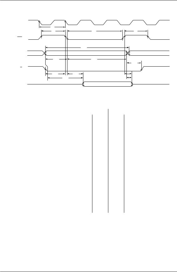
SPECIFICATIONS |
|
|
|
6.3.3. Display memory read timing |
|
|
|
EXTΦ0 |
|
|
|
tC |
|
|
|
tW |
|
tCE |
tW |
VCE |
|
|
|
|
|
tCYR |
|
VA0 to VA15 |
|
|
|
tASC |
|
tAHC |
|
|
|
|
tRCH |
VR/W |
|
|
|
tRCS |
tCEA |
|
tCE3 |
tACV |
|
|
tOH2 |
VD0 to VD7 |
|
|
|
Ta = –20 to 75°C
Signal |
Symbol |
|
|
|
|
Parameter |
VDD = 4.5 to 5.5V |
VDD = 2.7 to 4.5V |
Unit |
Condition |
||||||||
|
|
|
|
|
|
|
|
|
||||||||||
Min. |
|
Max. |
Min. |
Max. |
||||||||||||||
|
|
|
|
|
|
|
|
|
|
|
|
|
|
|
||||
|
|
|
|
|
|
|
|
|
|
|
|
|
|
|
|
|
|
|
EXT φ0 |
tC |
|
Clock period |
100 |
|
— |
125 |
— |
ns |
|
||||||||
|
|
|
|
|
|
|
|
HIGH-level |
|
|
|
|
|
|
|
|||
|
|
|
tW |
VCE |
tC – 50 |
|
— |
t C – 50 |
— |
ns |
|
|||||||
|
|
|
|
pulsewidth |
|
|
||||||||||||
|
|
|
|
|
|
|
|
|
|
|
|
|||||||
VCE |
|
|
|
|
|
|
|
|
||||||||||
|
|
|
|
|
|
|
|
|
|
|
|
|
|
|
|
|||
|
|
|
|
|
|
|
|
|
|
|
|
|
|
|
|
|||
tCE |
|
VCE LOW-level |
2tC – 30 |
|
— |
2t C – 30 |
— |
ns |
|
|||||||||
|
|
|
|
|
|
|||||||||||||
|
|
|
|
pulsewidth |
|
|
||||||||||||
|
|
|
|
|
|
|
|
|
|
|
|
|||||||
|
|
|
|
|
|
|
|
|
|
|
|
|
|
|
|
|
|
|
|
|
|
tCYR |
|
Read cycle time |
3tC |
|
— |
3t C |
— |
ns |
|
||||||
VA0 to |
tASC |
|
Address setup time to |
tC – 70 |
|
— |
t C – 100 |
— |
ns |
|
||||||||
|
falling edge of VCE |
|
|
|||||||||||||||
VA15 |
|
|
|
|
|
|
|
|
CL = 100 |
|||||||||
|
|
|
|
|
|
|
|
|
|
|
|
|
|
|
||||
tAHC |
|
Address hold time from |
2tC – 30 |
|
— |
2t C – 40 |
— |
ns |
||||||||||
|
|
|
|
|
||||||||||||||
|
|
|
|
|
pF |
|||||||||||||
|
|
|
|
|
|
|
|
|
|
|
|
|||||||
|
|
|
falling edge of VCE |
|
||||||||||||||
|
|
|
|
|
|
|
|
|
|
|
||||||||
|
|
|
tRCS |
|
Read cycle setup time to |
tC – 45 |
|
— |
t C – 60 |
— |
ns |
|
||||||
|
|
|
|
|
|
|
|
|
|
|
|
|
||||||
|
|
|
falling edge of VCE |
|
|
|||||||||||||
|
|
|
|
|
|
|
|
|
|
|
||||||||
VRD |
|
|
|
|
|
|
|
|
||||||||||
tRCH |
|
Read cycle hold time |
0.5tC |
|
— |
0.5t C |
— |
ns |
|
|||||||||
|
|
|
|
|
|
|||||||||||||
|
|
|
|
|
|
|
|
|
|
|
|
|
||||||
|
|
|
|
from rising edge of VCE |
|
|
||||||||||||
|
|
|
|
|
|
|
|
|
|
|
|
|||||||
|
|
|
tACV |
|
Address access time |
— 3t C – 100 |
— 3t C – 115 |
ns |
|
|||||||||
|
|
|
|
|
|
|
|
|
|
|
|
|
|
|
|
|
|
|
|
tCEA |
|
|
access time |
— |
2t C – 80 |
— |
2t C – 90 |
ns |
|
||||||||
VD0 to |
|
VCE |
|
|||||||||||||||
|
VD7 |
tOH2 |
|
Output data hold time |
0 |
|
— |
0 |
— |
ns |
|
|||||||
|
|
|
|
|
|
|
|
|
|
|
|
|
|
|
|
|
|
|
|
|
|
tCE3 |
|
|
to data off time |
0 |
|
— |
0 |
— |
ns |
|
|||||
|
|
|
|
VCE |
|
|
||||||||||||
12 |
EPSON |
S1D13305 Series
Technical Manual
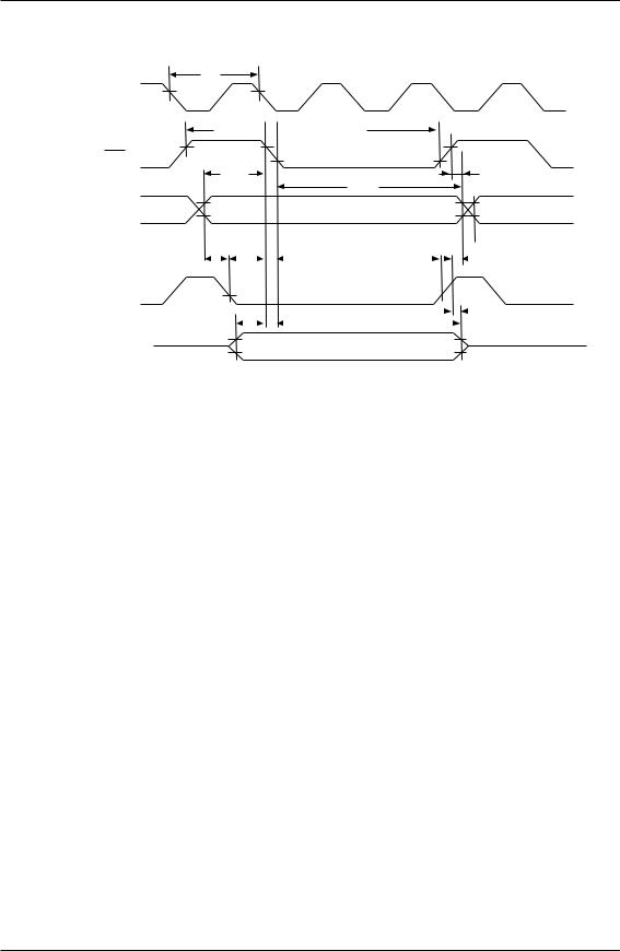
SPECIFICATIONS
6.3.4. Display memory write timing
tC
EXT φ O
tW 
 tCE
tCE
VCE
tASC |
tCA |
tAHC
VA0 to VA15
|
|
|
tAS |
tWSC |
|
|
|
|
|
|||||||||||
|
|
|
|
|
|
|
|
|
tWHC |
|
|
|
|
|
|
|
tAH2 |
|||
|
|
|
|
|
|
|
|
|
|
|
|
|
|
|||||||
|
|
|
|
|
|
|
|
|
|
|
|
|
|
|
|
|
|
|
|
|
|
|
|
|
|
|
|
|
|
|
|
|
|
|
|
|
|
|
|
||
VR/W |
|
|
|
|
|
|
|
|
|
|
|
|
|
|
tDH2 |
|||||
tDSC |
|
|
|
|
||||||||||||||||
|
|
|
|
|
|
|
|
|
||||||||||||
|
|
|
|
|
|
|
|
|
||||||||||||
|
|
|
|
|
|
|
|
|
|
tDHC |
|
|
|
|
|
|
||||
|
|
|
|
|
|
|
|
|
|
|
|
|
|
|
|
|||||
VD0 to VD7
S1D13305 Series
Technical Manual
EPSON |
13 |

SPECIFICATIONS
Ta = –20 to 75°C
Signal |
Symbol |
|
|
Parameter |
VDD = 4.5 to 5.5V |
VDD = 2.7 to 4.5V |
Unit |
Condition |
||||||||||
|
|
Min. |
Max. |
Min. |
Max. |
|||||||||||||
|
|
|
|
|
|
|
|
|
|
|
|
|
|
|||||
|
|
|
|
|
|
|
|
|
|
|
|
|
|
|
|
|
|
|
EXT φ0 |
tC |
Clock period |
100 |
— |
125 |
— |
ns |
|
||||||||||
|
|
|
|
|
|
|
|
|
|
|
|
|
|
|
|
|
|
|
|
|
|
|
|
|
|
HIGH-level |
|
|
|
|
|
|
|||||
|
|
|
|
tW |
VCE |
tC – 50 |
— |
t C – 50 |
— |
ns |
|
|||||||
|
|
|
|
pulsewidth |
|
|||||||||||||
|
|
|
|
|
|
|
|
|
|
|
||||||||
|
VCE |
|
|
|
|
|
|
|
||||||||||
|
|
|
|
|
|
|
|
|
|
|
|
|
|
|
||||
|
|
|
|
|
|
|
|
|
|
|
|
|
|
|||||
tCE |
VCE LOW-level |
2tC – 30 |
— |
2t C – 30 |
— |
ns |
|
|||||||||||
|
|
|
|
|
||||||||||||||
|
|
|
|
pulsewidth |
|
|||||||||||||
|
|
|
|
|
|
|
|
|
|
|
||||||||
|
|
|
|
|
|
|
|
|
|
|
|
|
|
|
|
|
|
|
|
|
|
|
tCYW |
Write cycle time |
3tC |
— |
3t C |
— |
ns |
|
|||||||
|
|
|
|
|
|
|
|
|
|
|
|
|
|
|
|
|||
|
|
|
|
tAHC |
Address hold time from |
2tC – 30 |
— |
2t C – 40 |
— |
ns |
|
|||||||
|
|
|
|
|
|
|
|
|
|
|
|
|||||||
|
|
|
|
falling edge of VCE |
|
|||||||||||||
|
|
|
|
|
|
|
|
|
|
|
||||||||
|
|
|
|
tASC |
Address setup time to |
tC – 70 |
— |
t C – 110 |
— |
ns |
|
|||||||
|
|
|
|
|
|
|
|
|
|
|
|
|||||||
VA0 to |
falling edge of VCE |
|
||||||||||||||||
|
|
|
|
|
|
|
||||||||||||
tCA |
Address hold time from |
0 |
— |
0 |
— |
ns |
|
|||||||||||
VA15 |
CL = 100 |
|||||||||||||||||
rising edge of VCE |
||||||||||||||||||
|
|
|
|
|
|
|
|
|
|
|||||||||
|
|
|
|
|
|
|
|
|
|
|
|
|
|
|
|
|
pF |
|
|
|
|
|
tAS |
Address setup time to |
0 |
— |
0 |
— |
ns |
||||||||
|
|
|
|
|
||||||||||||||
|
|
|
|
|
|
|
|
|
|
|
|
|||||||
|
|
|
|
falling edge of VWR |
|
|||||||||||||
|
|
|
|
|
|
|
|
|
|
|
||||||||
|
|
|
|
tAH2 |
Address hold time from |
10 |
— |
10 |
— |
ns |
|
|||||||
|
|
|
|
|
|
|
|
|
|
|
|
|||||||
|
|
|
|
rising edge of VWR |
|
|||||||||||||
|
|
|
|
|
|
|
|
|
|
|
||||||||
|
|
|
|
tWSC |
Write setup time to |
tC – 80 |
— |
t C – 115 |
— |
ns |
|
|||||||
|
|
|
|
|
|
|
|
|
|
|
|
|||||||
|
|
|
|
falling edge of VCE |
|
|||||||||||||
|
|
|
|
|
|
|
|
|
|
|
||||||||
VWR |
|
|
|
|
|
|
|
|||||||||||
tWHC |
Write hold time from |
2tC – 20 |
— |
2t C – 20 |
— |
ns |
|
|||||||||||
|
|
|
|
|
||||||||||||||
|
|
|
|
|
|
|
|
|
|
|
|
|||||||
|
|
|
|
falling edge of VCE |
|
|||||||||||||
|
|
|
|
|
|
|
|
|
|
|
||||||||
|
|
|
|
tDSC |
Data input setup time to |
tC – 85 |
— |
t C – 125 |
— |
ns |
|
|||||||
|
|
|
|
falling edge of VCE |
|
|||||||||||||
|
|
|
|
|
|
|
|
|
|
|
||||||||
|
|
|
|
|
|
|
|
|
|
|
|
|
|
|
||||
VD0 to |
tDHC |
Data input hold time |
2tC – 30 |
— |
2t C – 30 |
— |
ns |
|
||||||||||
|
|
|
|
|
|
|
|
|
|
|
|
|||||||
|
|
VD7 |
from falling edge of VCE |
|
||||||||||||||
|
|
|
|
|
|
|
|
|
||||||||||
|
|
|
|
tDH2 |
Data hold time from |
5 |
50 |
5 |
50 |
ns |
|
|||||||
|
|
|
|
|
|
|
|
|
|
|
|
|||||||
|
|
|
|
rising edge of VWR |
|
|||||||||||||
|
|
|
|
|
|
|
|
|
|
|
||||||||
Note: VD0 to VD7 are latching input/outputs. While the bus is high impedance, VD0 to VD7 retain the write data until the data read from the memory is placed on the bus.
14 |
EPSON |
S1D13305 Series
Technical Manual
SPECIFICATIONS
6.3.5. SLEEP IN command timing
|
|
|
|
|
|
|
|
|
|
|
|
|
VCE |
|
|
|
|
|
|
|
|
|
|
|
|
SLEEP IN write |
SYSTEM SET write |
|
||||||||||
|
|
|
|
tWRL |
|
|
|
|
tWRD |
|
|
|
|
|
|
|
|
|
|
|
|
|
|
||
WR
(Command input)
YDIS
Ta = –20 to 75°C
Signal |
Symbol |
|
|
Parameter |
VDD = 4.5 to 5.5V |
VDD = 2.7 to 4.5V |
Unit |
Condition |
|||||
|
|
Min. |
Max. |
Min. |
Max. |
||||||||
|
|
|
|
|
|
|
|
|
|||||
|
|
|
|
|
|
|
|
|
|
|
|
|
|
|
|
|
|
|
|
falling-edge delay |
|
|
|
|
|
|
|
|
|
|
tWRD |
VCE |
See note 1. |
— |
See note 1. |
— |
ns |
|
|||
|
|
|
time |
CL = 100 |
|||||||||
|
|
|
|
|
|
|
|
|
|||||
WR |
|
|
|
|
|
|
|||||||
tWRL |
YDIS falling-edge delay |
— |
See note 2. |
— |
See note 2. |
ns |
pF |
||||||
|
|
|
|||||||||||
|
|
|
time |
|
|||||||||
|
|
|
|
|
|
|
|
|
|
||||
Notes: |
|
|
|
|
|
|
|
|
|
||||
1.tWRD = 18tC + tOSS + 40 (tOSS is the time delay from the sleep state until stable operation)
2.tWRL = 36tC × [TC/R] × [L/F] + 70
S1D13305 Series
Technical Manual
EPSON |
15 |
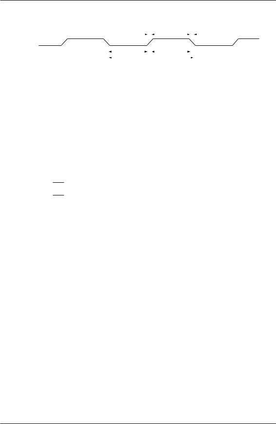
SPECIFICATIONS
6.3.6. External oscillator signal timing
EXTφ0 |
|
|
|
|
|
|
|
|
|
|
|
|
|
|
tRCL |
|
|
|
|
|
|
|
|
|
|
|
tFCL |
|
|
|
|
|
|
|
|
|
|
|
|
|
|
|
|
|
|
|
|
|
|
|
|
||||
|
|
|
|
|
|
|
|
|
|
|
|
|
|
|
|
|
|
|
|
|
|
|
|
|
|
|
|
|
|
|
|
|
|
|
|
|
|
|
|
|
|
|
|
|
|
|
|
|
|
|
|
|
|||
|
|
|
|
|
tWL |
|
|
|
|
|
|
|
|
|
|
tWH |
|
|
|
|
|
|
|
||||
|
|
|
|
|
|
|
|
|
|
|
|
|
|
|
|
|
|
|
|
|
|
||||||
|
|
|
|
|
|
|
|
|
|
|
|
|
|
|
|
|
|
|
|
|
|
|
|
||||
|
|
|
|
|
|
|
|
|
|
tC |
|
|
|
|
|
|
|
|
|
|
|
|
|
|
|
||
|
|
|
|
|
|
|
|
|
|
|
|
|
|
|
|
|
|
|
|
|
|
|
|
|
|||
|
|
|
|
|
|
|
|
|
|
|
|
|
|
|
|
|
|
|
|
|
|
|
|
|
|
|
|
Ta = –20 to 75°C
Signal |
Symbol |
Parameter |
VDD = 4.5 to 5.5V |
VDD = 2.7 to 4.5V |
|
Unit |
Condition |
||
|
|
|
|
|
|||||
Min. |
Max. |
Min. |
Max |
|
|||||
|
|
|
|
|
|
||||
|
tRCL |
External clock rise time |
— |
15 |
— |
15 |
|
ns |
|
|
|
|
|
|
|
|
|
|
|
|
tFCL |
External clock fall time |
— |
15 |
— |
15 |
|
ns |
|
|
|
|
|
|
|
|
|
|
|
EXT φ0 |
tWH |
External clock |
See note 1. |
See note 2. |
See note 1. |
See note 2. |
|
ns |
|
HIGH-level pulsewidth |
|
|
|||||||
|
|
|
|
|
|
|
|
|
|
|
|
|
|
|
|
|
|
|
|
|
tWL |
External clock |
See note 1. |
See note 2. |
See note 1. |
See note 2. |
|
ns |
|
|
LOW-level pulsewidth |
|
|
||||||
|
|
|
|
|
|
|
|
|
|
|
|
|
|
|
|
|
|
|
|
|
tC |
External clock period |
100 |
— |
125 |
— |
|
ns |
|
Notes:
1.(tC – tRCL – tFCL) × 1000475
2.(tC – tRCL – tFCL) × 1000525
< tWH, tWL
> tWH, tWL
16 |
EPSON |
S1D13305 Series
Technical Manual
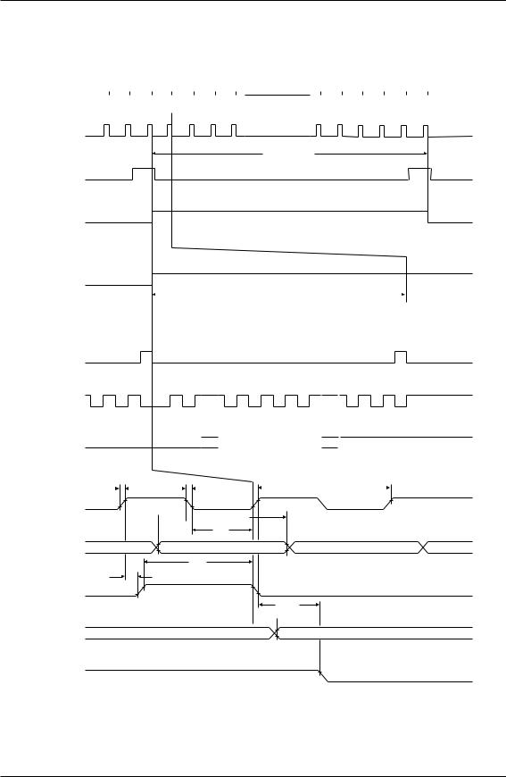
SPECIFICATIONS
6.3.7. LCD output timing
The following characteristics are for a 1/64 duty cycle.
Row |
62 |
63 |
64 |
1 |
2 |
3 |
4 |
|
60 |
61 |
62 |
63 |
64 |
LP
1 frame time
YD
WF
WF
|
|
|
|
|
|
|
|
|
|
|
|
|
1 line time |
|
|
|
|
|
|
|
|
|
|
|
|
|
|
|
|
|
|
|
|
|
|
|
|
|
|
|
|
||
Row 64 |
|
|
|
|
|
|
|
|
|
|
Row 1 |
|
|
|
|
Row 2 |
|||||
LP |
|
|
|
|
|
|
|
|
|
|
|
|
|
|
|
|
|
|
|
|
|
XSCL |
|
|
|
|
|
|
|
|
|
|
|
|
|
|
|
|
|
|
|
||
|
|
|
|
|
|
|
|
|
|
|
|
|
|
|
|
|
|
|
|
|
|
XD0 to XD3 (14) (15) |
(16) |
|
|
(1) |
|
|
|
|
(15)(16)(1) (2) (3) |
|
|
|
(15) (16) |
(1) |
|||||||
|
tr |
|
|
|
tWX |
|
|
|
|
tf |
|
|
|
|
|
tCX |
|
|
|
||
|
|
|
|
|
|
|
|
|
|
|
|
|
|
|
|
||||||
XSCL
 tDS
tDS 
 tDH
tDH
tLS
XD0 to XD3
tWL
tLD
LP
tDHY
 tDF
tDF
WF(B)
YD
S1D13305 Series
Technical Manual
EPSON |
17 |

SPECIFICATIONS
Ta = –20 to 75°C
Signal |
Symbol |
Parameter |
VDD = 4.5 to 5.5V |
|
VDD = 2.7 to 4.5V |
Unit |
Condition |
|||
|
|
|
|
|
|
|||||
Min. |
Max. |
|
|
Min. |
Max |
|||||
|
|
|
|
|
|
|
||||
|
|
|
|
|
|
|
|
|
|
|
|
tr |
Rise time |
— |
30 |
|
|
— |
40 |
ns |
|
|
|
|
|
|
|
|
|
|
|
|
|
tf |
Fall time |
— |
30 |
|
|
— |
40 |
ns |
|
|
|
|
|
|
|
|
|
|
|
|
XSCL |
tCX |
Shift clock cycle time |
4tC |
— |
|
|
4t C |
— |
ns |
|
tWX |
XSCL clock pulsewidth |
2tC – 60 |
— |
|
2t |
C – 60 |
— |
ns |
|
|
|
|
|
||||||||
|
|
|
|
|
|
|
|
|
|
|
XD0 to |
tDH |
X data hold time |
2tC – 50 |
— |
|
2t |
C – 50 |
— |
ns |
CL = |
XD3 |
tDS |
X data setup time |
2tC – 100 |
— |
2t C – 105 |
— |
ns |
100 pF |
||
|
|
|
|
|
|
|
|
|
|
|
|
tLS |
Latch data setup time |
2tC – 50 |
— |
2t |
C – 50 |
— |
ns |
|
|
|
|
|
|
|
|
|
|
|
||
LP |
tWL |
LP pulsewidth |
4tC – 80 |
— |
4t C – 120 |
— |
ns |
|
||
|
tLD |
LP delay time from XSCL |
0 |
— |
|
|
0 |
— |
ns |
|
|
|
|
|
|
|
|
|
|
|
|
WF |
tDF |
Permitted WF delay |
— |
50 |
|
|
— |
50 |
ns |
|
|
|
|
|
|
|
|
|
|
|
|
YD |
tDHY |
Y data hold time |
2tC – 20 |
— |
2t |
C – 20 |
— |
ns |
|
|
18 |
EPSON |
S1D13305 Series
Technical Manual
PACKAGE DIMENSIONS
7. PACKAGE DIMENSIONS
Unit: mm
7.1. S1D13305F00A
àQFP5-60 pin
|
25.6 ± 0.4 |
|
20.0 ± 0.1 |
54 |
36 |
55 |
35 |
60 |
|
Index |
30 |
± 0.1 |
± 0.4 |
1 |
|
29 |
14.0 |
19.6 |
|
|
|
||||
|
|
|
|
||
5 |
|
|
24 |
|
|
|
|
|
|
|
|
|
|
6 |
23 |
|
|
0.15 ± 0.05 |
2.7 ± 0.1 |
1.0 ± 0.1 |
0.35 ± 0.1 |
|
|
|
|
|
|
||
|
|
|
1.5 ± 0.3 |
0 to 12° |
|
|
|
|
|
||
|
|
|
2.8 |
|
|
7.2. S1D13305F00B
àQFP6-60 pin
|
|
17.6 ± 0.4 |
|
|
|
|
|
14.0 ± 0.2 |
|
|
|
|
|
45 |
|
31 |
|
|
46 |
|
|
30 |
|
|
|
Index |
14.0 ± 0.2 |
17.6 ± 0.4 |
|
|
|
|
|
||
|
60 |
|
|
16 |
|
0.15±0.05 |
2.7±0.1 |
1 |
|
15 |
|
0.8 |
± 0.15 |
0.35 ± 0.15 |
|
||
|
|
|
|||
|
|
|
|
|
0 to 12° |
|
|
|
|
0.8 ± 0.3 |
|
|
|
|
|
1.8 |
|
S1D13305 Series
Technical Manual
EPSON |
19 |

INSTRUCTION SET
8. INSTRUCTION SET
8.1. The Command Set
Table 1. |
Command set |
|
|
|
|
|
|
|
|
|
|
|
|
|
|
|
|
|
|
|
|
|
|
|
|
|
|
|
|
|
|
|
|
|
|
|
|
|
|
Command |
|
|
|
|
|
|
|
|
|
|
Code |
|
|
|
|
|
|
|
Read |
|||
Class |
Command |
|
|
|
|
|
|
|
|
|
|
|
|
|
|
|
Hex |
Command Description |
Parameters |
|
|
|
|
|
|
|
|
|
|
|
|
|
|
|
|
|
|
|
|
No. of |
Sec- |
|
|
RD |
WR |
A0 |
D7 |
D6 |
D5 |
D4 |
D3 |
D2 |
D1 |
D0 |
|
|
||||||
|
|
|
|
Bytes |
tion |
|||||||||||||||
|
|
|
|
|
|
|
|
|
|
|
|
|
|
|
|
|
|
|
||
|
|
|
|
|
|
|
|
|
|
|
|
|
|
|
|
|
|
|
|
|
System |
SYSTEM SET |
1 |
|
0 |
1 |
0 |
1 |
|
0 |
|
0 |
0 |
0 |
0 |
0 |
40 |
Initialize device and |
8 |
8.2.1 |
|
control |
|
|
|
|
|
|
|
|
|
|
|
|
|
|
|
|
|
display |
|
|
SLEEP IN |
1 |
|
0 |
1 |
0 |
1 |
|
0 |
|
1 |
0 |
0 |
1 |
1 |
53 |
Enter standby mode |
0 |
8.2.2 |
||
|
|
|
|
|||||||||||||||||
|
DISP ON/OFF |
1 |
|
0 |
1 |
0 |
1 |
|
0 |
|
1 |
1 |
0 |
0 |
D |
58, |
Enable and disable dis- |
1 |
8.3.1 |
|
|
|
|
|
59 |
play and display flashing |
|||||||||||||||
|
|
|
|
|
|
|
|
|
|
|
|
|
|
|
|
|
|
|
||
|
|
|
|
|
|
|
|
|
|
|
|
|
|
|
|
|
|
|
|
|
|
SCROLL |
1 |
|
0 |
1 |
0 |
1 |
|
0 |
|
0 |
0 |
1 |
0 |
0 |
44 |
Set display start address |
10 |
8.3.2 |
|
|
|
|
|
and display regions |
||||||||||||||||
|
CSRFORM |
1 |
|
0 |
1 |
0 |
1 |
|
0 |
|
1 |
1 |
1 |
0 |
1 |
5D |
Set cursor type |
2 |
8.3.3 |
|
|
|
|
|
|
|
|
|
|
|
|
|
|
|
|
|
|
|
|
|
|
Display |
CGRAM ADR |
1 |
|
0 |
1 |
0 |
1 |
|
0 |
|
1 |
1 |
1 |
0 |
0 |
5C |
Set start address of char- |
2 |
8.3.6 |
|
control |
|
|
|
|
|
|
|
|
|
|
|
|
|
|
|
|
|
acter generator RAM |
|
|
|
|
|
|
|
|
|
|
|
|
|
|
|
|
CD |
CD |
4C |
Set direction of cursor |
|
|
|
|
|
|
|
|
|
|
|
|
|
|
|
|
|
|
|
|
||||
|
CSRDIR |
1 |
|
0 |
1 |
0 |
1 |
|
0 |
|
0 |
1 |
1 |
to |
0 |
8.3.4 |
||||
|
|
|
|
|
|
|
|
|
|
|
|
|
|
|
1 |
0 |
4F |
movement |
|
|
|
|
|
|
|
|
|
|
|
|
|
|
|
|
|
|
|
|
|
|
|
|
HDOT SCR |
1 |
|
0 |
1 |
0 |
1 |
|
0 |
|
1 |
1 |
0 |
1 |
0 |
5A |
Set horizontal scroll |
1 |
8.3.7 |
|
|
|
|
|
position |
||||||||||||||||
|
|
|
|
|
|
|
|
|
|
|
|
|
|
|
|
|
|
|
|
|
|
OVLAY |
1 |
|
0 |
1 |
0 |
1 |
|
0 |
|
1 |
1 |
0 |
1 |
1 |
5B |
Set display overlay |
1 |
8.3.5 |
|
|
|
|
|
format |
||||||||||||||||
|
|
|
|
|
|
|
|
|
|
|
|
|
|
|
|
|
|
|
|
|
Drawing |
CSRW |
1 |
|
0 |
1 |
0 |
1 |
|
0 |
|
0 |
0 |
1 |
1 |
0 |
46 |
Set cursor address |
2 |
8.4.1 |
|
control |
CSRR |
1 |
|
0 |
1 |
0 |
1 |
|
0 |
|
0 |
0 |
1 |
1 |
1 |
47 |
Read cursor address |
2 |
8.4.2 |
|
|
|
|
|
|
|
|
|
|
|
|
|
|
|
|
|
|
|
|
|
|
Memory |
MWRITE |
1 |
|
0 |
1 |
0 |
1 |
|
0 |
|
0 |
0 |
0 |
1 |
0 |
42 |
Write to display memory |
— |
8.5.1 |
|
|
|
|
|
|
|
|
|
|
|
|
|
|
|
|
|
|
|
|
|
|
|
|
|
|
|
|
|
|
|
|
|
|
|
|
|
|
|
Read from display |
|
|
|
control |
MREAD |
1 |
|
0 |
1 |
0 |
1 |
|
0 |
|
0 |
0 |
0 |
1 |
1 |
43 |
— |
8.5.2 |
||
|
|
|
memory |
|||||||||||||||||
|
|
|
|
|||||||||||||||||
|
|
|
|
|
|
|
|
|
|
|
|
|
|
|
|
|
|
|
|
|
Notes:
1.In general, the internal registers of the S1D13305 series are modified as each command parameter is input. However,
the microprocessor does not have to set all the parameters of a command and may send a new command before all parameters have been input. The internal registers for the parameters that have been input will have been changed but the remaining parameter registers are unchanged.
2-byte parameters (where two bytes are treated as 1 data item) are handled as follows:
a.CSRW, CSRR: Each byte is processed individually. The microprocessor may read or write just the low byte of the cursor address.
b.SYSTEM SET, SCROLL, CGRAM ADR: Both parameter bytes are processed together. If the command is changed after half of the parameter has been input, the single byte is ignored.
2.APL and APH are 2-byte parameters, but are treated as two 1-byte parameters.
20 |
EPSON |
S1D13305 Series
Technical Manual

INSTRUCTION SET
8.2. System Control Commands
8.2.1. SYSTEM SET
Initializes the device, sets the window sizes, and selects the LCD interface format. Since this command sets the basic operating parameters of the S1D13305 series, an
incorrect SYSTEM SET command may cause other commands to operate incorrectly.
|
MSB |
|
|
|
|
|
|
|
|
|
|
|
|
|
|
LSB |
|
|
|
|
|
|
|||||
|
|
|
D7 |
D6 |
D5 |
D4 |
|
D3 |
D2 |
D1 |
D0 |
|
|
|
A0 |
WR |
RD |
||||||||||
|
|
|
|
|
|
|
|
|
|
|
|
|
|
|
|
|
|
|
|
|
|
|
|
|
|
|
|
C |
|
0 |
1 |
0 |
0 |
|
0 |
0 |
0 |
|
0 |
1 |
0 |
|
1 |
|
|||||||||||
|
|
|
|
|
|
|
|
|
|
|
|
|
|
|
|
|
|
|
|
|
|
|
|
|
|
|
|
|
|
|
|
|
|
|
|
|
|
|
|
|
|
|
|
|
|
|
|
|
|
|
|
|
|
|
|
P1 |
|
0 |
0 |
IV |
1 |
|
W/S |
M2 |
M1 |
M0 |
0 |
0 |
|
1 |
|
||||||||||||
|
|
|
|
|
|
|
|
|
|
|
|
|
|
|
|
|
|
|
|
|
|
|
|
|
|
|
|
|
|
|
|
|
|
|
|
|
|
|
|
|
|
|
|
|
|
|
|
|
|
|
|
|
|
|
|
P2 |
|
|
WF |
0 |
0 |
0 |
|
0 |
|
|
|
|
FX |
|
|
|
0 |
0 |
|
1 |
|
||||||
|
|
|
|
|
|
|
|
||||||||||||||||||||
|
|
|
|
|
|
|
|
|
|
|
|
|
|
|
|
|
|
|
|
|
|
|
|
|
|
|
|
|
|
|
|
|
|
|
|
|
|
|
|
|
|
|
|
|
|
|
|
|
|
|
|
|
|
|
|
P3 |
|
0 |
0 |
0 |
0 |
|
|
|
|
|
|
|
FY |
|
|
|
0 |
0 |
|
1 |
|
||||||
|
|
|
|
|
|
|
|
|
|
||||||||||||||||||
|
|
|
|
|
|
|
|
|
|
|
|
|
|
|
|
|
|
|
|
|
|
|
|
|
|
|
|
|
|
|
|
|
|
|
|
|
|
|
|
|
|
|
|
|
|
|
|
|
|
|
|
|
|
|
|
P4 |
|
|
|
|
|
|
|
C/R |
|
|
|
|
|
|
|
|
0 |
0 |
|
1 |
|
||||||
|
|
|
|
|
|
|
|
|
|
|
|
|
|
|
|||||||||||||
|
|
|
|
|
|
|
|
|
|
|
|
|
|
|
|
|
|
|
|
|
|
|
|
|
|
|
|
|
|
|
|
|
|
|
|
|
|
|
|
|
|
|
|
|
|
|
|
|
|
|
|
|
|
|
|
P5 |
|
|
|
|
|
|
|
TC/R |
|
|
|
|
|
|
|
|
0 |
0 |
|
1 |
|
||||||
|
|
|
|
|
|
|
|
|
|
|
|
|
|
|
|||||||||||||
|
|
|
|
|
|
|
|
|
|
|
|
|
|
|
|
|
|
|
|
|
|
|
|
|
|
|
|
|
|
|
|
|
|
|
|
|
|
|
|
|
|
|
|
|
|
|
|
|
|
|
|
|
|
|
|
P6 |
|
|
|
|
|
|
|
L/F |
|
|
|
|
|
|
|
|
0 |
0 |
|
1 |
|
||||||
|
|
|
|
|
|
|
|
|
|
|
|
|
|
|
|||||||||||||
|
|
|
|
|
|
|
|
|
|
|
|
|
|
|
|
|
|
|
|
|
|
|
|
|
|
|
|
|
|
|
|
|
|
|
|
|
|
|
|
|
|
|
|
|
|
|
|
|
|
|
|
|
|
|
|
P7 |
|
|
|
|
|
|
|
APL |
|
|
|
|
|
|
|
|
0 |
0 |
|
1 |
|
||||||
|
|
|
|
|
|
|
|
|
|
|
|
|
|
|
|||||||||||||
|
|
|
|
|
|
|
|
|
|
|
|
|
|
|
|
|
|
|
|
|
|
|
|
|
|
|
|
|
|
|
|
|
|
|
|
|
|
|
|
|
|
|
|
|
|
|
|
|
|
|
|
|
|
|
|
P8 |
|
|
|
|
|
|
|
APH |
|
|
|
|
|
|
|
|
|
|
0 |
0 |
|
1 |
|
||||
|
|
|
|
|
|
|
|
|
|
|
|
|
|
|
|
|
|||||||||||
|
|
|
|
|
|
|
|
|
|
|
|
|
|
|
|
|
|
|
|
|
|
|
|
|
|
|
|
Figure 1. SYSTEM SET instruction
8.2.1.1. C
This control byte performs the following:
1.Resets the internal timing generator
2.Disables the display
3.Cancels sleep mode
Parameters following P1 are not needed if only canceling sleep mode.
8.2.1.2. M0
Selects the internal or external character generator ROM. The internal character generator ROM contains 160, 5 × 7 pixel characters, as shown in figure 70. These characters are fixed at fabrication by the metallization mask. The external character generator ROM, on the other hand, can contain up to 256 user-defined characters.
M0 = 0: Internal CG ROM
M0 = 1: External CG ROM
Note that if the CG ROM address space overlaps the display memory address space, that portion of the display memory cannot be written to.
8.2.1.3. M1
Selects the memory configuration for user-definable characters. The CG RAM codes select one of the 64 codes shown in figure 46.
M1 = 0: No D6 correction.
The CG RAM1 and CG RAM2 address spaces are not contiguous, the CG RAM1 address space is treated as character generator RAM, and the CG RAM2 address space is treated as character generator ROM.
M1 = 1: D6 correction.
The CG RAM1 and CG RAM2 address spaces are contiguout and are both treated as character generator RAM.
S1D13305 Series
Technical Manual
EPSON |
21 |
INSTRUCTION SET
8.2.1.4. M2
Selects the height of the character bitmaps. Characters more than 16 pixels high can be displayed by creating a bitmap for each portion of each character and using the S1D13305 series graphics mode to reposition them.
M2 = 0: 8-pixel character height (2716 or equivalent ROM)
M2 = 1: 16-pixel character height (2732 or equivalent ROM)
8.2.1.5. W/S
Selects the LCD drive method. W/S = 0: Single-panel drive W/S = 1: Dual-panel drive
EI |
|
|
X driver |
|
X driver |
|
|||||
|
|
|
|
|
|
YD
Y driver |
LCD |
Figure 2. Single-panel display
EI |
X driver |
X driver |
YD |
|
|
|
|
Upper Panel |
Y driver |
|
|
|
|
Lower Panel |
|
X driver |
X driver |
Figure 3. Above and below two-panel display
22 |
EPSON |
S1D13305 Series
Technical Manual
INSTRUCTION SET
|
EI |
|
|
X driver |
|
X driver |
|
|
X driver |
|
X driver |
|
YD |
|
|
|
|
|
|
|
|
|
|
|
|
|
|
|
|
|
|
|
|
|
|
|
||
|
|
|
|
|
|
|
|
|
|
|
|
|
|
|
|
|
|
|
|
|
|
|
|
|
|
|
|
|
|
|
|
|
|
|
|
|
|
|
Y driver |
|
|
|
Left Panel |
|
|
|
Right Panel |
|
|||
|
|
|
|
|
|
|
|
|
||||
|
|
|
|
|
|
|
|
|
|
|
|
|
|
|
|
|
|
|
|
|
|
|
|
|
|
Figure 4. Left-and-right two-panel display
Note
There are no Seiko Epson LCD units in the configuration shown in Figure 4.
Table 2. LCD parameters
Parameter |
W/S = 0 |
W/S = 1 |
|||
IV = 1 |
IV = 0 |
IV = 1 |
IV = 0 |
||
|
|||||
|
|
|
|
|
|
C/R |
C/R |
C/R |
C/R |
C/R |
|
TC/R |
TC/R |
TC/R (See note 1.) |
TC/R |
TC/R |
|
|
|
|
|
|
|
L/F |
L/F |
L/F |
L/F |
L/F |
|
|
|
|
|
|
|
SL1 |
00H to L/F |
00H to L/F + 1 |
(L/F) / 2 |
(L/F) / 2 |
|
(See note 2.) |
|||||
|
|
|
|
||
|
|
|
|
|
|
SL2 |
00H to L/F |
00H to L/F + 1 |
(L/F) / 2 |
(L/F) / 2 |
|
(See note 2.) |
|||||
|
|
|
|
||
|
|
|
|
|
|
SAD1 |
First screen block |
First screen block |
First screen block |
First screen block |
|
|
|
|
|
|
|
SAD2 |
Second screen block |
Second screen block |
Second screen block |
Second screen block |
|
|
|
|
|
|
|
SAD3 |
Third screen block |
Third screen block |
Third screen block |
Third screen block |
|
|
|
|
|
|
|
SAD4 |
Invalid |
Invalid |
Fourth screen block |
Fourth screen block |
|
|
|
|
|
|
|
Cursor move- |
Continuous movement over whole screen |
Above-and-below configuration: |
|||
ment range |
continuous movement over whole screen |
||||
|
|
||||
|
|
|
|
|
|
Notes:
1.See table 26 for further details on setting the C/R and TC/R parameters when using the HDOT SCR command.
2.The value of SL when IV = 0 is equal to the value of SL when IV = 1, plus one.
8.2.1.6. IV
Screen origin compensation for inverse display. IV is usually set to 1.
The best way of displaying inverted characters is to Exclusive-OR the text layer with the graphics background layer. However, inverted characters at the top or
left of the screen are difficult to read as the character origin is at the top-left of its bitmap and there are no background pixels either above or to the left of these characters.
S1D13305 Series
Technical Manual
EPSON |
23 |
 Loading...