

Page 1
Ordering number : ENN6203
LB1868M
Monolithic Digital IC
LB1868M
Two-Phase Brushless Fan Motor Driver
Overview
The LB1868M is a 2-phase unipolar brushless motor
driver. With only a few peripheral parts, lockup protection
and automatic recovery can be implemented. The IC can
be configured for 12V or 24V operation and a wide range
of variations, from LOW speed to H-High speed and from
60 cm to 120 cm square using the same PCB. This makes
it easy to design highly reliable fan motor installations.
Functions and Features
• Output protection Zener diode with variable withstand
voltage
Z1, Z2 pins open: V
Z1, Z2 pins shorted: V
External Zener diode connected between Z1 and V
pins: support for fans with large drive current
• External resistor allows configuration for 12V or 24V.
• Direct Hall element connection possible (built-in Hall
amplifier with hysteresis supports core without auxiliary
electrode)
• Built-in output transistor with 1.0A output current
(strengthened negative-current support for core without
auxiliary electrode)
• Built-in rotation detection function:
Low during rotation and High during stop
• Built-in lockup protection with automatic recovery
• ST pin for motor stop/drive (for standby mode of copiers
etc.)
• FG output pin for rotation detection
• BC pin for kickback noise reduction (with 2 external
capacitors)
• Built-in thermal shutdown
= 57V (24V specification)
OLM
= 32V (12V specification)
OLM
CC
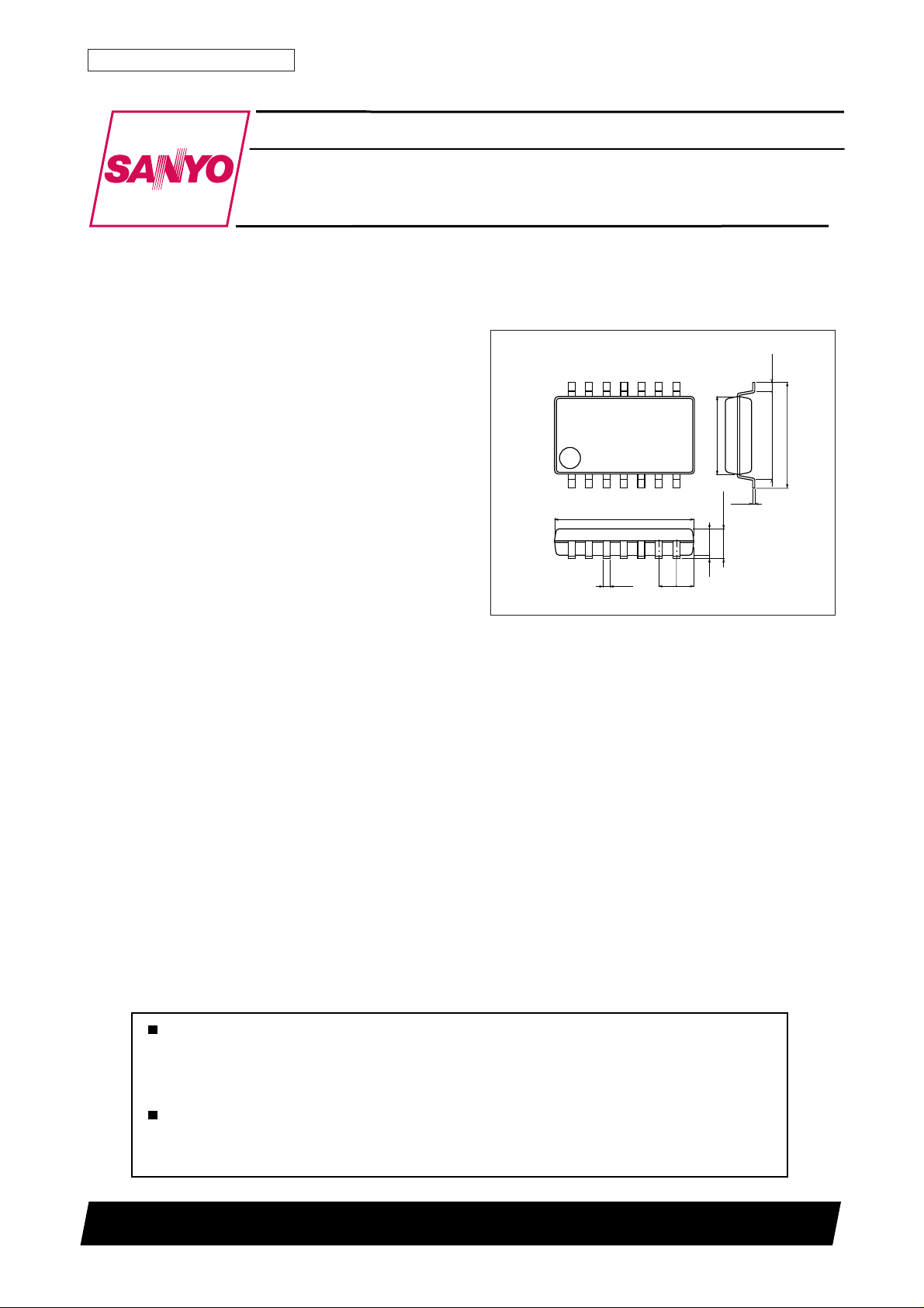
Package Dimensions
unit: mm
3111-MFP14S
[LB1868M]
14
1
8.0
1.0
0.35
8
4.4
7
1.8max
1.50.1
1.0
0.625
6.4
5.15
0.15
SANYO : MFP14S
Any and all SANYO products described or contained herein do not have specifications that can handle
applications that require extremely high levels of reliability, such as life-support systems, aircraft's
control systems, or other applications whose failure can be reasonably expected to result in serious
physical and/or material damage. Consult with your SANYO representative nearest you before using
any SANYO products described or contained herein in such applications.
SANYO assumes no responsibility for equipment failures that result from using products at values that
exceed, even momentarily, rated values (such as maximum ratings, operating condition ranges, or other
parameters) listed in products specifications of any and all SANYO products described or contained
herein.
SANYO Electric Co.,Ltd. Semiconductor Company
TOKYO OFFICE Tokyo Bldg., 1-10, 1 Chome, Ueno, Taito-ku, TOKYO, 110-8534 JAPAN
83100RM(KI)
No. 6203-1/5
Page 2

LB1868M
Specifications
Absolute Maximum Ratings at Ta = 25˚C
Parameter Symbol Conditions Ratings Unit
Maximum input current ICC max t ≤ 20 ms 200 mA
Maximum applied output voltage V
Maximum output current I
Current flowing into RD, FG IRD max 10 mA
RD, FG applied voltage VRD max 30 V
ST applied voltage VST max 7.5 V
Allowable power dissipation Pd max *With specified substrate 800 mW
Operating temperature Topr –30 to +80 °C
Storage temperature Tstg –55 to +150 °C
*Printed circuit board: 20 × 15 × 1.5 mm3 glass epoxy
max Internal V
OUT
max 1.0 A
OUT
0.9
With 20 × 15 × 1.5 mm3 glass epoxy
0.8
0.7
0.6
0.5
0.4
0.3
0.2
Allowable power dissipation, Pd max – W
0.1
0
Pd max – Ta
100806040200–20–30
Ambient temperature, Ta – °C
Allowable Operating Ranges at Ta = 25˚C
Parameter Symbol Conditions Ratings Unit
Input voltage range I
CC
Common mode input voltage range VICM 0.2 to VIN–1.5 V
ST High voltage VSTH 4.5 to 7.0 V
ST Low voltage VSTL 0 to 0.5 V
6.0 to 50 mA
Electrical Characteristics at Ta = 25˚C, Icc = 10 mA
Parameter Symbol Conditions
Output limiter withstand voltage V
1 Z1, Z2 open 54 57 60 V
OLM
V
2 Z1, Z2 short 31 33 35 V
OLM
Output saturation voltage Vosat 1 Io = 0.5A 0.95 1.2 V
2 Io = 1.0A 0.15 1.5 V
VIN voltage V
Hall input sensitivity (at zero peak) V
ICC = 7.0 mA 6.4 6.7 7.0 V
IN
Including offset and hysteresis 20 mV
HN
RD, FG output saturation voltage VRDsat IRD = 5 mA 0.1 0.3 V
CT drain current IC1 C = GND 2.7 3.8 4.9 µA
CT discharge current IC2 C = VIN 0.19 0.30 0.41 µA
Comp input threshold voltage VTH1 0.77
VTH2 0.42
ST input current I
Thermal protection circuit operating
temperature
TSD Design target value* 180 °C
VST = 5V 80 120 µA
ST
Thermal protection circuit hysteresis ∆TSD Design target value* 40 °C
* Design target values are not measured.
Ratings
min typ max
0.8V
0.45V
IN
IN
0.83 V
0.48 V
Unit
No. 6203-2/5
Page 3

LB1868M
Block Diagram and Sample Application Circuit
D
R1
R2
IN+
IN–
ST
C1
VIN
H
Constant
current
source
CT
Thermal
shutdown
OUT1
Control block
OUT2
L2L1
BC
Z1
Z2
FG
0.47 to 10 µF
Truth Table
ST IN+ IN– CT OUT1 OUT2 RD FG
HHLLHHL L
LHLHHLH
LHLLHLLL
or L H L L H L H
OPEN H L H H H H L
LHHHHHH
*RD is a latch type output.
RD
GND
No. 6203-3/5
Page 4

LB1868M
Pin Description
Pin name Function
IN– Hall input + pin Hysteresis amplifier
IN+ Hall input – pin Hysteresis amplifier
CT Lockup protection time setting capacitor pin (0.47 to 4.7 µF)
Z1 External Zener diode pin (external Zener diode to be connected between power supply and Z1)
Z2 Kickback absorption voltage alteration pin (shorted to Z1: 12V operation)
OUT1 Output 1 pin
OUT2 Output 2 pin
VIN Regulated power supply input pin (limiting resistor to be inserted between power supply and VIN)
GND GND pin
RD Lockup detection pin (latch type)
FG Rotation frequency detector pin
ST Start/stop pin
BC Output transistor common base pin
Pin Assignment
IN–
IN+
CT
ST
BC
OUT1
GND
Sample Application Circuits
(1) 12V supply voltage
Vcc
12V
2 kΩ
1
2
3
LB1868M
4
5
6
7
330 Ω
14 13 12 11 10 9 8
VINHRD FG Z2 Z1 OUT2
14
13
12
11
10
9
8
Top view
VIN
RD
FG
Z2
Z1
OUT2
NC
LB1868M
IN– IN+ CT ST BC OUT1 GND
64 5321 7
0.47 µF
No. 6203-4/5
Page 5

(2) 24V supply voltage
Vcc
1.2 kΩ
24V
14 13 12 11 10 9 8
2 kΩ
VIN RD FG Z2 Z1 OUT2
IN–HIN+ CT ST BC OUT1 GND
(3) High-Power Fan (120 mm-HH-speed)
Vcc
330 Ω
12V
(1.2 kΩ)
(24V)
LB1868M
LB1868M
674 5321
0.47 µF
VZ = 12V
(24V)
2 kΩ
14 13 12 11 10 9 8
VIN RD FG Z2 Z1 OUT2
LB1868M
IN– IN+ CT ST BC OUT1 GND
64 5321
7
H
Specifications of any and all SANYO products described or contained herein stipulate the performance,
characteristics, and functions of the described products in the independent state, and are not guarantees
of the performance, characteristics, and functions of the described products as mounted in the customer's
products or equipment. To verify symptoms and states that cannot be evaluated in an independent device,
the customer should always evaluate and test devices mounted in the customer's products or equipment.
SANYO Electric Co., Ltd. strives to supply high-quality high-reliability products. However, any and all
semiconductor products fail with some probability. It is possible that these probabilistic failures could
give rise to accidents or events that could endanger human lives, that could give rise to smoke or fire,
or that could cause damage to other property. When designing equipment, adopt safety measures so
that these kinds of accidents or events cannot occur. Such measures include but are not limited to protective
circuits and error prevention circuits for safe design, redundant design, and structural design.
In the event that any or all SANYO products(including technical data,services) described or
contained herein are controlled under any of applicable local export control laws and regulations,
such products must not be exported without obtaining the export license from the authorities
concerned in accordance with the above law.
No part of this publication may be reproduced or transmitted in any form or by any means, electronic or
mechanical, including photocopying and recording, or any information storage or retrieval system,
or otherwise, without the prior written permission of SANYO Electric Co. , Ltd.
Any and all information described or contained herein are subject to change without notice due to
product/technology improvement, etc. When designing equipment, refer to the "Delivery Specification"
for the SANYO product that you intend to use.
Information (including circuit diagrams and circuit parameters) herein is for example only ; it is not
guaranteed for volume production. SANYO believes information herein is accurate and reliable, but
no guarantees are made or implied regarding its use or any infringements of intellectual property rights
or other rights of third parties.
0.47 µF
This catalog provides information as of August, 2000. Specifications and information herein are subject to change
without notice.
No. 6203-5/5
PS
 Loading...