

Page 1

Ordering number : ENN4384A
LB1841V
Monolithic Digital IC
LB1841V
Low-Saturation Current-Controlled
Forward/Reverse Motor Driver
Overview
The LB1841V is a low-saturation current-controlled
forward/reverse motor driver with provision for a constant
voltage circuit using an external transistor and an output
current limiter function. Its design is optimized for use in
video camera loading motors.
Features
• Built-in output current limiter and detector circuit
• Built-in low-saturation voltage forward/reverse bridge
circuit: VOsat = 0.40V typ. at 400 mA
• Little current drain in standby mode
(up to 0.1 µA)
• Built-in low-saturation constant voltage circuit using an
external pnp transistor
• Built-in reference voltage linked to input
• Built-in thermal shutdown circuit
• Low external parts count. Compact SSOP-20 package
allows space saving design.
Package Dimensions
unit: mm
3179A-SSOP20
[LB1841V]
20
110
6.7
11
0.650.22 0.43
4.4
0.15
1.6max
0.1
SANYO : SSOP20
1.0
6.4
0.5
Specifications
Absolute Maximum Ratings at Ta = 25°C
Parameter Symbol Conditions Ratings Unit
Maximum supply voltage VCC max 10.5 V
Maximum output current Im max 800 mA
Applied input voltage V
Allowable power dissipation Pd max With substrate (50 × 35 × 1.6 mm3) 800 mW
Operating temperature Topr –20 to +80 °C
Storage temperature Tstg –40 to +150 °C
Any and all SANYO products described or contained herein do not have specifications that can handle
applications that require extremely high levels of reliability, such as life-support systems, aircraft's
control systems, or other applications whose failure can be reasonably expected to result in serious
physical and/or material damage. Consult with your SANYO representative nearest you before using
any SANYO products described or contained herein in such applications.
SANYO assumes no responsibility for equipment failures that result from using products at values that
exceed, even momentarily, rated values (such as maximum ratings, operating condition ranges, or other
parameters) listed in products specifications of any and all SANYO products described or contained
herein.
IN
–0.3 to +10 V
SANYO Electric Co.,Ltd. Semiconductor Company
TOKYO OFFICE Tokyo Bldg., 1-10, 1 Chome, Ueno, Taito-ku, TOKYO, 110-8534 JAPAN
73099RM(KI)
No. 4384-1/7
Page 2

LB1841V
Allowable Operating Ranges at Ta = 25°C
Parameter Symbol Conditions Ratings Unit
Power supply voltage V
Input High voltage V
Input Low voltage V
SVR input voltage V
LIR input voltage V
Output current limiter I
CC
IH
IL
SVR
LIR
limit
Electrical Characteristics at Ta = 25°C, VCC = 7.2V
Parameter Symbol Conditions
Power supply current ICC 0 In standby mode 0.1 10 µA
ICC 1 Forward/reverse No load 9 13 mA
ICC 2 In brake mode 12 18 mA
Output saturation voltage Vsat 1 IO = 200 mA (upper side + lower side) 0.20 0.30 V
Vsat 2 IO = 400 mA (upper side + lower side) 0.40 0.60 V
Reference voltage Vref I
Current limiter characteristics I
Input current I
PBC drive current I
Vs output voltage V
limit
IN
PBC
S
= 1 mA 1.85 2.0 2.15 V
Vref
VS-VM resistance = 1Ω at LIR = 2V 165 185 205 mA
VIN = 5V 90 150 µA
RD saturation voltage VRDsat IO = 1 mA 0.3 V
min typ max
3.0 to 9.0 V
3.0 to 9.0 V
–0.3 to 0.7 V
1.0 to VCC–0.2 V
0.5 to VCC–1.0 V
50 to 350 mA
Ratings
–10 mA
2.55×V
SVR
Unit
V
Constant-voltage output VS is determined by the equation VS = 2.55 × V
The input range of V
is 1.0 to 4 V. When VS ≥ VCC, the output will be saturated.
SVR
SVR
.
The output current limiter value is determined according to the following equation (Rf is a sensing resistor across VS and VM).
I limit = V
V
input range is 0.5 to VCC –1.0 (V).
LIR
/10 Rf(A)
LIR
Block Diagram and Sample Application Circuit
VCC = 3 to 10.5V
10µF
SVR
LIR
VS = 5.1V
10µF
cc
PBC V
S
V
= 0.47 to 2Ω
R
f
V
M
OUT1
0.001µF
to 0.01µF
OUT2
P-G
M
Vref
= 2.0V
Thermal
shutdown
S-G
DECODER
RD
Limit
detection
DELIN2IN1
No. 4384-2/7
Page 3

Pin Assignment
P-GND
OUT1
OUT1
V
LB1841V
1
2
3
4
M
20
19
18
17
P-GND
OUT2
OUT2
LIR
V
5
Note) • VM (motor power supply/sensing pin)
are both connected.
• P-GND (motor power supply GND pin)
are both connected.
• S-GND (control power supply ground
V
PBC
V
V
NC
M
S
CC
ref
LB1841V
6
7
8
9
10
pin) is connected to microprocessor
ground.
Truth Table
Bridge and VS circuits
Input Output
IN1 IN2 OUT1 OUT2 V
L L off off off Standby
H L H L H Forward rotation
L H L H H Reverse rotation
H H L L off Brake
Output current limiter and detection output
DEL OUT output RD
H
limit L
Non-limit off
L Saturation off
S
16
15
14
13
12
11
(Top view)
Mode
SVR
DEL
IN2
IN1
RD
S-GND
Pd max – Ta
1000
Specified substrate (50×35×1.6 mm3, glass epoxy)
800
600
400
200
Allowable power dissipation, Pd max – mW
0
–20 0 20 40 60 80 100
Ambient temperature, Ta – °C
No. 4384-3/7
Page 4
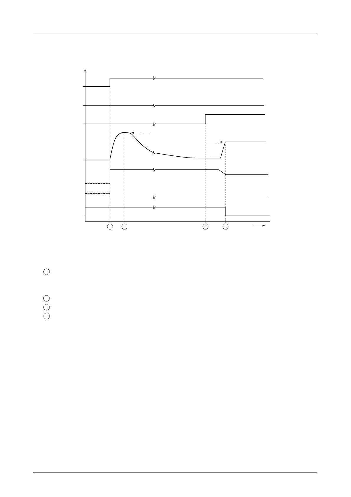
Sample Application Timing Chart
V(V)
IN1
IN2
DEL
IO
G
OUT1
OUT2
V
M
R
LB1841V
V
10R
LIR
f
RD
1 2 3 4
t (s)
• Sample Application timing chart
1 Connect DC motor (RL = RΩ) between OUT1 and OUT2, and input forward signal (IN1 = High, IN2 = Low)
with RD pin in pull-up state.
Because output is saturated during startup, set DEL input to Low.
2 DC motor starts and startup current (IST = VM/R) flows through motor.
3 DC motor rotates in normal condition. At this point, set DEL input to High.
4 When DC motor locks up, motor current IM increases. When it reaches I
limit
(=V
/(10 Rf)), output current
LIR
limiting circuit operates. At the same time, the set current detection circuit sets RD output to Low.
• Reference voltage Vref
The Vref output is linked to the input. When IN1 or IN2 is High, the reference voltage is output.
• Output current limiter circuitry
The circuit configuration is as shown in the separate diagram.
The output set current is determined by the reference voltage V
applied to the LIR pin. When V
LIR
applied, 1/10 of the voltage occurs across RS in the diagram. This voltage is input to the + side of the voltage
setting amplifier.
The motor current IM generates a voltage (IM × Rf) across the external resistor Rf. This voltage is input to
the – side of the amplifier. The differential amplifier operates so as to make the two inputs equal, then the
output transistor is driven.
The set current is determined by the following equation:
I
limit
= V
/(10Rf) [A]
LIR
LIR
is
No. 4384-4/7
Page 5
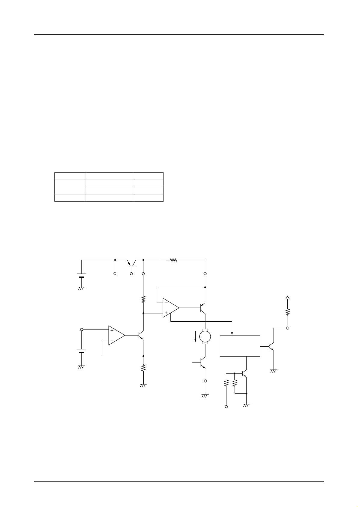
• Set current detection circuit
(1) When DEL = High
When the motor current IM is below the set current I
setting amplifier is smaller than the input voltage at the + side (larger vs. ground). The drive current therefore
increases and the output pnp transistor saturates. When this condition is detected, a signal is sent to the set
current detection circuit and the RD output becomes High.
When the motor current IM reaches the set current I
the RD output becomes Low.
(2) When DEL = Low
When a Low signal is input to the DEL pin, operation of the current setting amplifier is canceled. Therefore as
described above, the output transistor saturates and the RD output becomes High.
The above conditions are shown in the table below.
DEL OUT RD
H
L Saturation H
Non-limit (saturation) H
limit L
LB1841V
limit
limit
, the input voltage (IM × Rf) at the – side of the current
, the output pnp transistor is in the controlled state and
Output Current Limiter and Setting Current Detection Circuits Block Diagram
R
f
V
V
CC
LIR
V
LIR
V
PBC
CC
10R
S
R
S
I
M
S
P-G
M
V
M
Setting current
detection circuit
DEL
R
D
No. 4384-5/7
Page 6
LB1841V
16
LIR = SVR = Vref
VIN = 5.0V
14
Rf = 0.5Ω, no load
12
– mA
10
CC
8
6
Current drain, I
4
2
0
01 2 345
Power supply voltage, VCC – V
6
VIN = 5.0V
SVR = Vref
5
– V
S
4
3
2
output voltage, V
S
V
1
ICC – V
CC
Brake
DEL = L
DEL = H
6 7 8 9 10 1211
VS – V
CC
Forward/reverse
Forward/
reverse
240
200
160
– µA
IN
120
80
Input current, I
40
0
012 345
Input voltage, VIN – V
10
VCC = 8.0V
V
= 3.0V
IN
LIR = Vref
8
– V
S
6
4
output voltage, V
S
V
2
IIN – V
IN
6 7 8 9 10 11
VS – V
SVR
VCC = 8.0V
0
012 345
Power supply voltage, VCC – V
600
I limit – V
VCC = 6.0V
SVR = Vref
500
R
= 10Ω
L
400
300
200
Output set current, I limit – mA
100
0
0 0.4 0.8 1.2 1.6 2.0
0.6
= 0.5Ω
f
R
1.0Ω
VO(sat) – I
VCC = 6.0V
V
= 3.0V
IN
0.5
LIR = SVR = Vref
DEL = L
(sat) – V
O
0.4
6 7 8 9 10 11
LIR
2.4 2.8 3.2 3.6 4.0 4.84.4
– V
LIR
O
0
0 0.4 0.8 1.2 1.6 2.0
SVR input voltage, V
400
I limit – V
SVR = Vref
V
= 3.0V
IN
R
= 10Ω
L
.
R
= 0.5Ω
.
f
300
200
100
Output set current, I limit – mA
0
01234
Power supply voltage, VCC – VV
0.4
VO(sat) – Ta
VCC = 6.0V
V
= 3.0V
IN
LIR = SVR = Vref
DEL = L
0.3
(sat) – V
O
2.4 2.8 3.2 3.6 4.0 4.84.4
SVR
– V
CC
Ilimit = 300mA
200mA
100mA
6789 1110
5
= 400mA
I
O
0.3
0.2
0.1
Output saturation voltage, V
0
0 100 200 300 400 500
Output current, IO – mA
600 700 800 900
0.2
0.1
Output saturation voltage, V
0
–40 –20 0 20 40
Ambient temperature, Ta – °C
200mA
60 80 100 120 160
140
No. 4384-6/7
Page 7
LB1841V
Specifications of any and all SANYO products described or contained herein stipulate the performance,
characteristics, and functions of the described products in the independent state, and are not guarantees
of the performance, characteristics, and functions of the described products as mounted in the customer's
products or equipment. To verify symptoms and states that cannot be evaluated in an independent device,
the customer should always evaluate and test devices mounted in the customer's products or equipment.
SANYO Electric Co., Ltd. strives to supply high-quality high-reliability products. However, any and all
semiconductor products fail with some probability. It is possible that these probabilistic failures could
give rise to accidents or events that could endanger human lives, that could give rise to smoke or fire,
or that could cause damage to other property. When designing equipment, adopt safety measures so
that these kinds of accidents or events cannot occur. Such measures include but are not limited to protective
circuits and error prevention circuits for safe design, redundant design, and structural design.
In the event that any or all SANYO products(including technical data,services) described or
contained herein are controlled under any of applicable local export control laws and regulations,
such products must not be exported without obtaining the export license from the authorities
concerned in accordance with the above law.
No part of this publication may be reproduced or transmitted in any form or by any means, electronic or
mechanical, including photocopying and recording, or any information storage or retrieval system,
or otherwise, without the prior written permission of SANYO Electric Co. , Ltd.
Any and all information described or contained herein are subject to change without notice due to
product/technology improvement, etc. When designing equipment, refer to the "Delivery Specification"
for the SANYO product that you intend to use.
Information (including circuit diagrams and circuit parameters) herein is for example only ; it is not
guaranteed for volume production. SANYO believes information herein is accurate and reliable, but
no guarantees are made or implied regarding its use or any infringements of intellectual property rights
or other rights of third parties.
This catalog provides information as of July, 1999. Specifications and information herein are subject to change
without notice.
No. 4384-7/7
PS
 Loading...