

Page 1
Ordering number : ENN6087A
21003AS (OT) / 52199RM (KI) No. 6087-1/12
Overview
The LB1975 is a three-phase brushless motor driver IC
suited for use in direct PWM driving of DC fan motors for
air conditioners, water heaters, and other similar
equipment. Since a shunt regulator circuit is built in,
single power supply operation sharing the same power
supply for the motor is supported.
Features
• Withstand voltage 45 V, output current 2.5 A
• Direct PWM drive output
• 3 built-in output top-side diodes
• Built-in current limiter
• Built-in FG output circuit
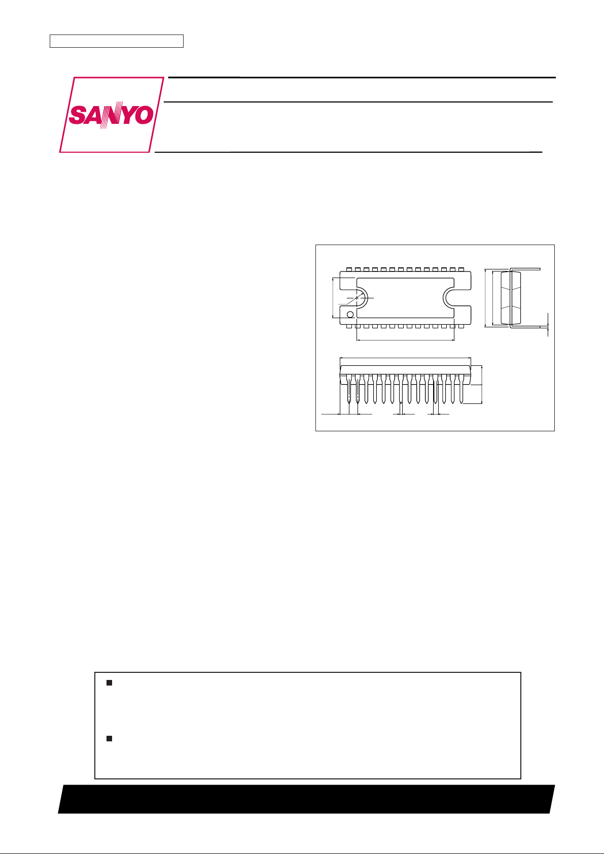
Package Dimensions
unit: mm
3147C-DIP28H
1
14
28
15
0.4
0.6
4.04.0
26.75
20.0
R1.7
8.4
(1.81)
1.78
1.0
12.7
11.2
SANYO: DIP28H
[LB1975]
LB1975
SANYO Electric Co.,Ltd. Semiconductor Company
TOKYO OFFICE Tokyo Bldg., 1-10, 1 Chome, Ueno, Taito-ku, TOKYO, 110-8534 JAPAN
DC Fan Motor Driver
Monolithic Digital IC
Any and all SANYO products described or contained herein do not have specifications that can handle
applications that require extremely high levels of reliability, such as life-support systems, aircraft’s
control systems, or other applications whose failure can be reasonably expected to result in serious
physical and/or material damage. Consult with your SANYO representative nearest you before using
any SANYO products described or contained herein in such applications.
SANYO assumes no responsibility for equipment failures that result from using products at values that
exceed, even momentarily, rated values (such as maximum ratings, operating condition ranges, or other
parameters) listed in products specifications of any and all SANYO products described or contained
herein.
Page 2
No. 6087-2/12
LB1975
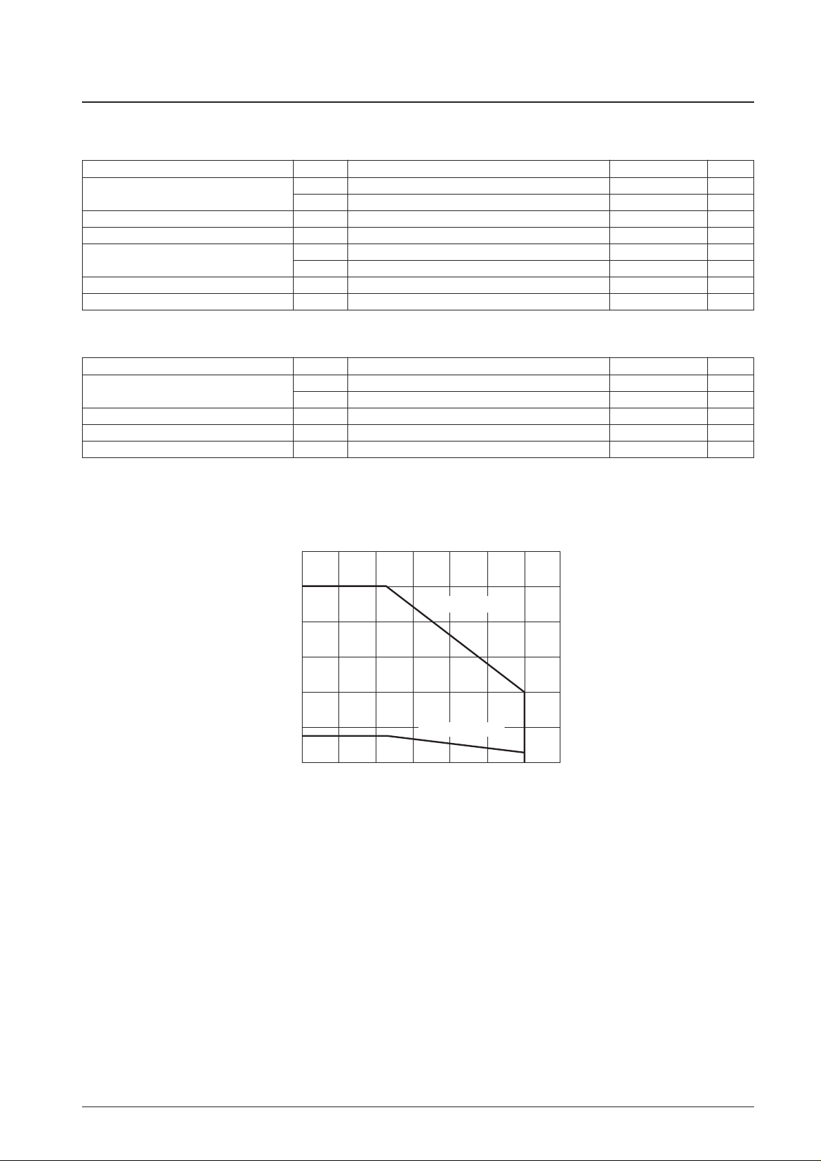
Parameter Symbol Conditions Ratings Unit
Supply voltage
V
CC
max 7 V
V
M
max 45 V
Output current I
O
max 2.5 A
Maximum input current I
REG
max V
REG
pin 10 mA
Allowable power dissipation
Pd max1 IC only 3 W
Pd max2 With infinite heat sink 20 W
Operating temperature Topr –20 to +100 °C
Storage temperature Tstg –55 to +150 °C
Specifications
Absolute Maximum Ratings at Ta = 25°C
Parameter Symbol Conditions Ratings Unit
Supply voltage range
V
CC
4.5 to 6.7 V
V
M
20 to 42 V
Input current range I
REG
V
REG
pin 1 to 5 mA
FG pin applied voltage V
FG
0 to V
CC
V
FG pin output current I
FG
0 to 10 mA
Allowable Operating Ranges at Ta = 25°C
3
0
4
8
12
16
20
24
–20 0 20 40 60 80 100 120
Allowable power dissipation, Pd max – W
Pd max – Ta
Ambient temperature, Ta – ˚C
With infinite heat sink
Independent IC
Page 3
No. 6087-3/12
LB1975
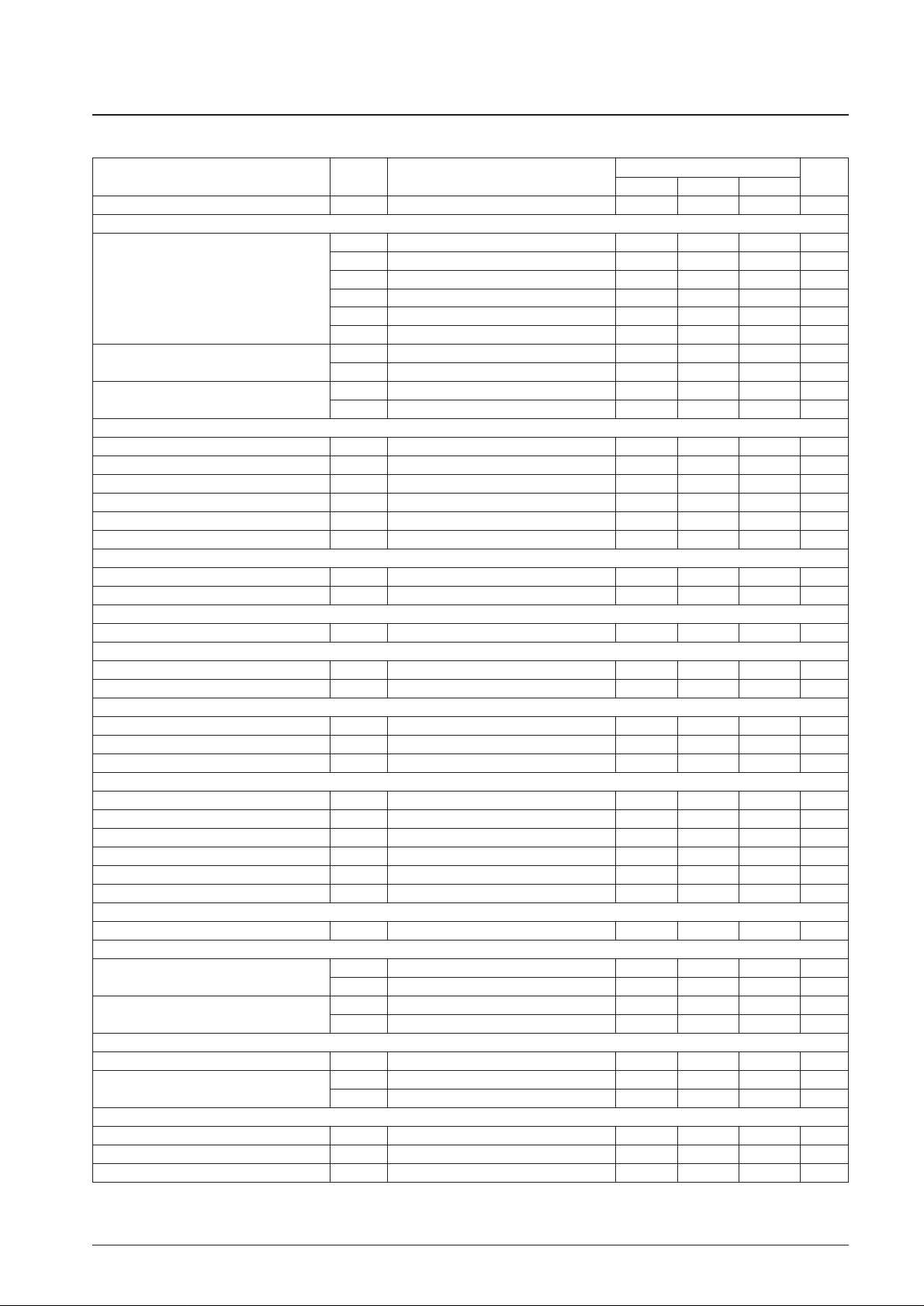
Parameter Symbol Conditions
Ratings
Unit
min typ max
Supply current I
CC
10 14 18 mA
[Output Block]
V
O
sat1 (L) IO= 1.0 A, VO(sink) 1.1 1.4 V
V
O
sat1 (H) IO= 1.0 A, VO(source) 0.9 1.3 V
Output saturation voltage
V
O
sat1 IO= 1.0 A, VO(sink) + VO(source) 2.0 2.6 V
V
O
sat2 (L) IO= 2.0 A, VO(sink) 1.4 1.8 V
V
O
sat2 (H) IO= 2.0 A, VO(source) 1.2 1.7 V
V
O
sat2 IO= 2.0 A, VO(sink) + VO(source) 2.6 3.4 V
Output leak current
I
O
Leak (L) 100 µA
I
O
Leak (H) –100 µA
Upper side diode forward voltage
V
FH
1 IO= 1.0 A 1.2 1.6 V
V
FH
2 IO= 2.0 A 2.1 2.6 V
[Hall Amplifier]
Input bias current I
HB
–4 –1 µA
Common-mode input voltage range V
ICM
1.5
VCC– 1.5
V
Hall input sensitivity VH
IN
60 mVp-p
Hysteresis width ∆V
IN
(HA) 23 32 39 mV
Input voltage (low to high) V
SLH
6 16 25 mV
Input voltage (high to low) V
SHL
–25 –16 –6 mV
[FG Pin (speed pulse output)]
Output low-level voltage V
FGLIFG
= 5 mA 0.5 V
Pull-up resistor value R
FG
7.5 10 12.5 kΩ
[Current Limiter]
Limiter V
RF
0.45 0.50 0.55 V
[Thermal Shutdown]
Thermal shutdown operating temperature TSD Desigh target Value (junction temperature) 150 180 °C
Hysteresis width ∆TSD Desigh target Value (junction temperature) 40 °C
[Low-Voltage Protection]
Operating voltage V
LVSD
3.5 3.8 4.1 V
Non-operating voltage
V
LVSD
(OFF)
4.3 4.5 V
Hysteresis width ∆V
LSD
0.4 0.5 0.6 V
[PWM Oscillator]
Output high-level voltage
VOH(OSC)
2.95 3.10 3.25 V
Output low-level voltage
VOL(OSC)
1.38 1.45 1.59 V
Amplitude V
OSC
1.50 1.65 1.71 Vp-p
Ocillator frequency f
OSC
C = 2200 pF 19.6 23.0 27.6 kHz
Charge current I
CHG
–110 –94 –83 µA
Discharge resistance R
DCHG
1.6 2.1 2.6 kΩ
[V
REG
Pin]
Pin voltage V
REGIREG
= 1.5 mA 6.6 7.0 7.2 V
[V
CTL
Pin]
Input voltage
V
CTL
1 Output duty 0% 1.1 1.4 1.7 V
V
CTL
2 Output duty 100% 3.2 3.5 3.8 V
Input bias current
I
B
1 (CTL) V
CTL
= 0 V –82 µA
I
B
2 (CTL) V
CTL
= 5 V 92 µA
[V
CTL
Amplifier]
Reference voltage V
CREF
2.23 2.35 2.46 V
Output voltage
V
COUT
1 V
CTL
= 0 V 3.90 4.20 4.40 V
V
COUT
2 V
CTL
= 5 V 0.60 0.80 1.10 V
[Start/Stop Pin]
High-level input voltage range V
IH
(S/S)
VCC– 1.5
V
CC
V
Low-level input voltage range V
IL
(S/S) 0 1.5 V
Input open voltage V
IO
(S/S)
VCC– 0.5
V
CC
V
Electrical Characteristics at Ta = 25°C, VCC= 5 V, VM= 30 V
Continued on next page.
Page 4
No. 6087-4/12
LB1975
Parameter Symbol Conditions
Ratings
Unit
min typ max
Hysteresis width ∆V
IN
(S/S) 0.35 0.50 0.65 V
High-level input current I
IH
(S/S) V (S/S) = V
CC
–10 0 10 µA
Low-level input current I
IL
(S/S) V (S/S) = 0 V –280 –210 µA
[Forward/Reverse Pin]
High-level input voltage range V
IH
(F/R)
VCC– 1.5
V
CC
V
Low-level input voltage range V
IL
(F/R) 0 1.5 V
Input open voltage V
IO
(F/R)
VCC– 0.5
V
CC
V
Hysteresis width ∆V
IN
(F/R) 0.35 0.50 0.65 V
High-level input current I
IH
(F/R) V (F/R) = V
CC
–10 0 10 µA
Low-level input current I
IL
(F/R) V (F/R) = 0 V –280 –210 µA
Continued from preceding page.
LB1975
V
COUT
VCCV
REG
S/S F/R (NC) OUT1 OUT2 OUT3 (NC) (NC) GND3 GND2 RF V
M
V
CTL
OSC (NC) V
CREF
IN1–IN1+IN2–IN2+IN3–IN3+FG1 FG2 GND1
1 2 3 4 5 6 7 8 9 10 11 12 13 14
28 27 26 25 24 23 22 21 20 19 18 17 16 15
Top view
A11950
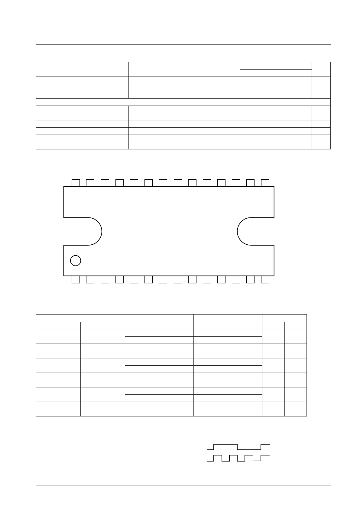
Pin Assignment
Truth Table
F/R
Forward rotation Low 0 V to 1.5 V
Reverse rotation High V
CC
– 1.5 V to V
CC
FG output
Input Forward/reverse control Output FG output
IN1 IN2 IN3 F/R Source
→ Sink FG1 FG2
1 H L H
L OUT2 → OUT1
L L
H OUT1 →OUT2
2 H L L
L OUT3 → OUT1
L H
H OUT1 →OUT3
3 H H L
L OUT3 → OUT2
L L
H OUT2 →OUT3
4 L H L
L OUT1 → OUT2
H H
H OUT2 →OUT1
5 L H H
L OUT1 → OUT3
H L
H OUT3 →OUT1
6 L L H
L OUT2 → OUT3
H H
H OUT3 →OUT2
FG1
FG2
Page 5
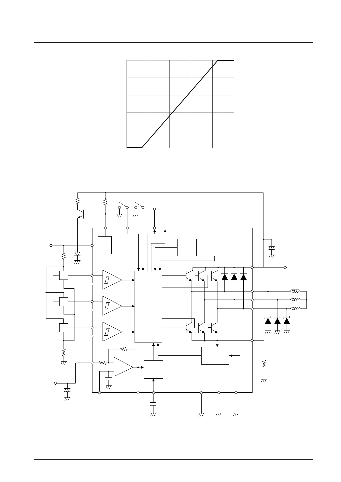
Block Diagram and Peripheral Circuit
No. 6087-5/12
LB1975
0
20
40
60
80
100
Duty — %
Duty – V
CTL
characteristics
Control voltage, V
CTL
— V
V
CTL
1 V
CTL
2
+
–
31 kΩ
2.35 V
40 kΩV
CTL
V
CC
Hys.Amp
V
CC
V
REG
Reg
LVSD TSD
S/S F/R FG1 FG2
V
M
OUT1
OUT2
OUT3
RF
V
M
IN3
IN2
IN1
V
CREF
V
CTL
V
COUT
OSC GND1 GND2 GND3
0.5 V
+
–
+
+
–
V
CTL
Amp
Rf
Current
limiter
Logic
PWM
OSC
+
+
–
A11952
+
Page 6
No. 6087-6/12
LB1975
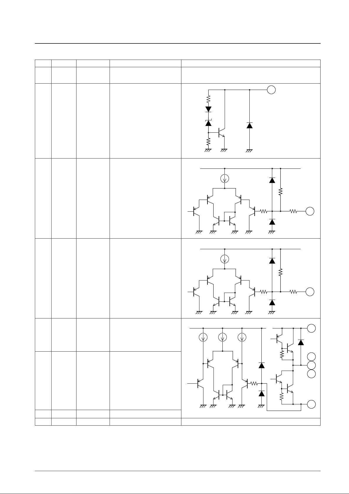
Pin Functions
Pin No. Pin name Pin voltage Pin function Equivalent circuit
Power supply for blocks other than
the output block
1
A11953
2
V
CC
4.5 V to 6.7 V
Shunt regulator output pin (7 V)2
V
REG
0.0 V to 7.3 V
A11954
3
V
CC
20 kΩ
3.8 kΩ
Start/stop control pin
Low: start
High or Open: stop
Typical threshold voltage for
V
CC
= 5 V:
approx. 2.8 V (low to high)
approx. 2.3 V (high to low)
3 S/S
0.0 V to V
CC
A11955
4
V
CC
20 kΩ
3.8 kΩ
Forward/reverse pin
Low: forward
High or Open: reverse
Typical threshold voltage for
V
CC
= 5 V:
approx. 2.8 V (low to high)
approx. 2.3 V (high to low)
4 F/R
0.0 V to V
CC
A11956
8
7
6
14
13
V
CC
200 Ω
0.5 V
V
M
Output pin 1
Output pin 2
Output pin 3
Output current detect pin. Connect
resistor RF between this pin and
ground. Output current is limited to
value set with V
RF
/Rf. (Current limiter
operation)
6
7
8
13
OUT1
OUT2
OUT3
RF
0.0 V to V
CC
Output block power supply14
V
M
Output block ground11 GND3
Continued on next page.
Page 7
No. 6087-7/12
LB1975
Continued from preceding page.
Pin No. Pin name Pin voltage Pin function Equivalent circuit
Ground for blocks other than the
output block
15
12
A11957
16 17
V
CC
10 kΩ
GND1
GND2
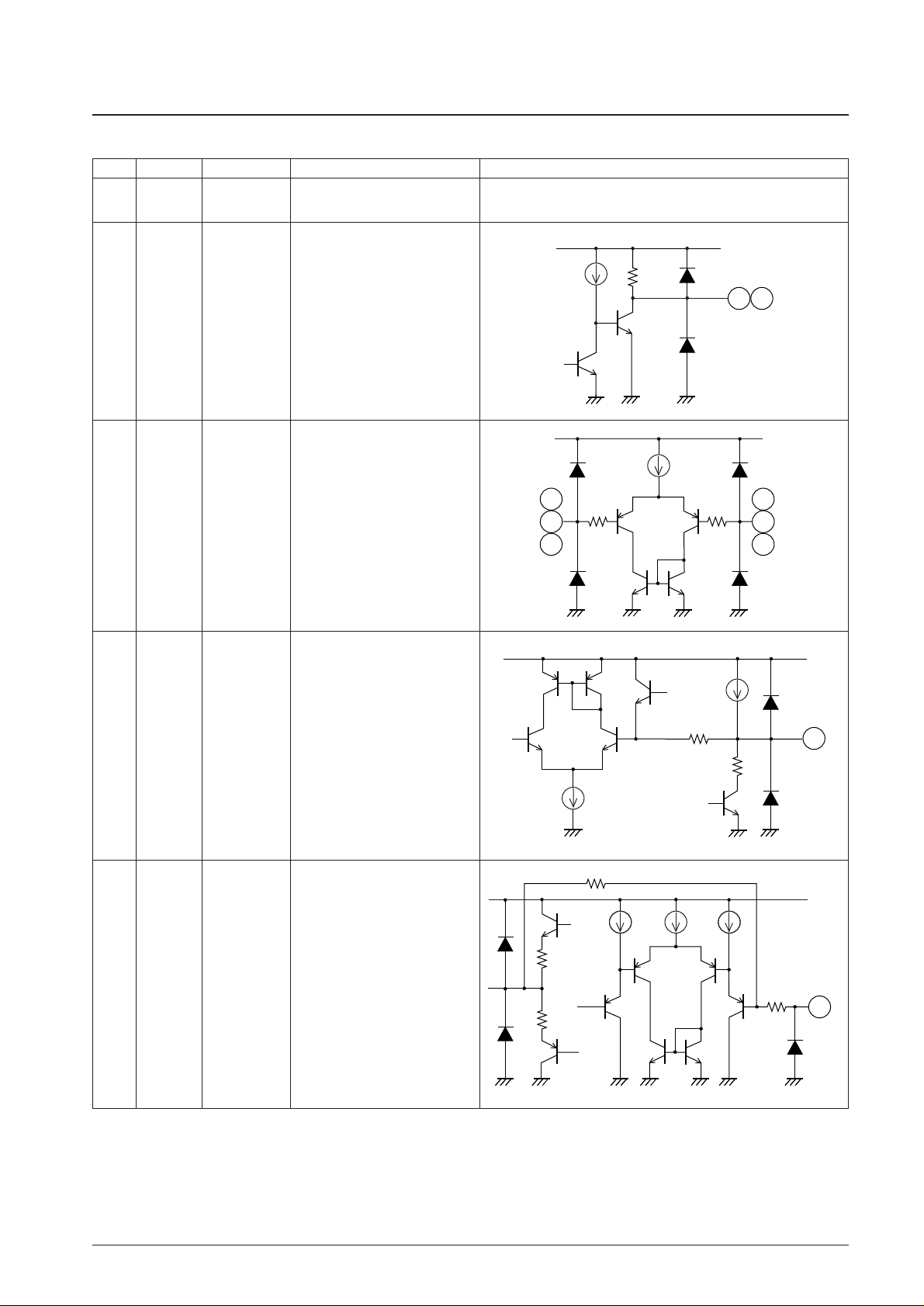
Speed pulse output pin 1 with built-in
pull-up resistor
Speed pulse output pin 2 with built-in
pull-up resistor
17
16
FG1
FG2
0.0 V to V
CC
A11958
V
CC
21
23
19
20
22
18
300 Ω300 Ω
Hall input pin
IN+> IN–: High input
IN+< IN–: Low input
22
23
20
21
18
19
IN1
+
IN1
–
IN2
+
IN2
–
IN3
+
IN3
–
1.5 V to
V
CC
– 1.5 V
26
A11959
V
CC
2 V
200 Ω
94 µA
2.1 kΩ
This pin sets the PWM oscillation
frequency. Connect a capacitor
between this pin and ground.
26 OSC
1.0 V to V
CC
27
A11960
V
CC
2.35 V
31 kΩ
40 kΩ
Output duty cycle control pin
• V
CTL
≤ V
CTL
1
Duty cycle 0%
• V
CTL
1 < V
CTL
< V
CTL
2
Duty cycle is controlled by V
CTL
• V
CTL
≥ V
CTL
2
Duty cycle 100%
27
V
CTL
0.0 V to 6.7 V
Continued on next page.
Page 8
No. 6087-8/12
LB1975
Continued from preceding page.
Pin No. Pin name Pin voltage Pin function Equivalent circuit
V
CTL
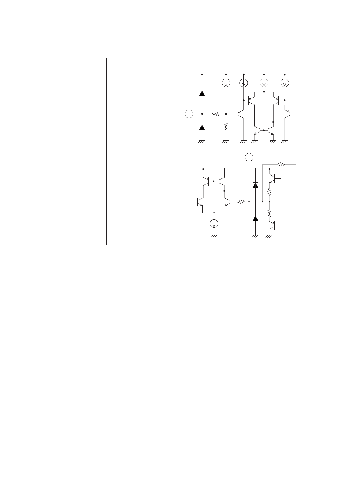
amplifier internal reference
voltage pin (2.35 V)
24
V
CREF
0.0 V to
V
CC
– 2.0 V
A11962
28
V
CC
200 Ω
31 kΩ
V
CTL
amplifier output pin
28
V
COUT
0.7 V to
V
CC
– 0.7 V
V
CC
100 µA
24
200 Ω
23.5 kΩ
A11961
Page 9

IC Description
Direct PWM Drive
This IC (LB1975) employs the direct PWM drive principle. Motor rotation speed is controlled by varying the output
duty cycle according to an analog voltage input (V
CTL
). This eliminates the need to alter the motor power supply
voltage. Compared to previous ICs using the PAM principle (such as the Sanyo LB1690), this allows simplification of
the power supply circuitry. The V
CTL
input can be directly supplied by a microcontroller, motor speed can, therefore, be
controlled directly from the microcontroller.
For PWM, the source-side output transistors are switched on and off so that the ON duty tracks the V
CTL
input. The
output duty cycle can be controlled over the range of 0% to 100% by the V
CTL
input.
PWM Frequency
The PWM oscillator frequency f
PWM
[Hz] is set by the capacitance C [pF] connected between the OSC pin and GND.
The following equation applies:
f
PWM
≈ 1 / (1.97 × C) × 10
8
Because output transistor on/off switching is subject to a delay, setting the PWM frequency to a very high value will
cause the delay to become noticeable. The PWM frequency therefore should normally be kept below 40 kHz (typ.),
which is achieved with a capacitance C of 1300 pF or higher. For reference, the source-side output transistor switching
delay time is about 2 µs for ON and about 4 µs for OFF.
Output Diodes
Because the PWM switching operation is carried out by the source-side output transistors, Schottky barrier diodes must
be connected between the OUT pins and GND (OUT1 to OUT3). Use diodes with an average forward current rating in
the range of 1.0 to 2.0 A, in accordance with the motor type and current limiting requirements.
If no Schottky barrier diodes are connected externally, or if Schottky barrier diodes with high forward voltage (VF) are
used, the internal parasitic diode between OUT and GND becomes active. When this happens, the output logic circuit
may malfunction, resulting in feedthrough current in the output which can destroy the output transistors. To prevent this
possibility, Schottky barrier diodes must be used and dimensioned properly.
The larger the VFof the externally connected Schottky barrier diodes, or the hotter the IC is, the more likely are the
parasitic diodes between OUT and GND to become active and the more likely is malfunction to occur. The VFof the
Schottky barrier diodes must be determined so that output malfunction does not occur also when the IC becomes hot. If
malfunction occurs, choose a Schottky barrier diode with lower VF.
Protection circuits
• Low voltage protection circuit
When the VCCvoltage falls below a stipulated level (V
LVSD
), the low voltage protection circuit cuts off the source-side
output transistors to prevent VCCrelated malfunction.
• Thermal shutdown circuit (overheat protection circuit)
When the junction temperature rises above a stipulated value (TSD), the thermal shutdown circuit cuts off the sourceside output transistors to prevent IC damage due to overheating. Design the application heat characteristics so that the
protection circuit will not be triggered under normal circumstances.
• Current limiter
The current limiter cuts off the source-side output transistors when the output current reaches a preset value (limiter
value). This interrupts the source current and thereby limits the output current peak value. By connecting the
resistance Rf between the RF pin and ground, the output current can be detected as a voltage. When the RF pin voltage
reaches 0.5 V (typ.), the current limiter is activated. It performs on/off control of the source-side output transistors,
thereby limiting the output current to the value determined by 0.5 /Rf.
No. 6087-9/12
LB1975
Page 10

Hall Input Circuit
The Hall input circuit is a differential amplifier with a hysteresis of 32 mV (typ.). The operation DC level must be within
the common-mode input voltage range (1.5V to VCC– 1.5 V). To prevent noise and other adverse influences, the input
level should be at least 3 times the hysteresis (120 to 160 mVp-p). If noise at the Hall input is a problem, a noisecanceling capacitor (about 0.01 µF) should be connected across the Hall input IN+and IN–pins.
FG Output Circuit
The Hall input signal at IN1, IN2, and IN3 is combined and subject to waveform shaping before being output. The signal
at FG1 has the same frequency as the FG1 Hall input, and the signal at FG2 has a frequency that is three times higher.
Start/Stop Control Circuit
The start/stop control circuit turns the source-side output transistors OFF (motor stop) when a High signal is input at the
S/S pin or when the pin is Open. When a Low signal is input at the S/S pin, the source-side output transistors are turned
ON, and the normal operation state is established (motor start).
Forward/Reverse Switching
This IC is designed under the assumption that forward/reverse switching is not carried out while the motor is running. If
switching is carried out while the motor is running, reverse torque braking occurs, leading to a high current flow. If the
current limiter is triggered, the source-side output transistors are switched off, and the sink-side output transistors go into
the short brake condition. However, because the current limiter of this IC cannot control the current flowing in the sinkside output transistors, these may be destroyed by the short brake current. Therefore F/R switching while the motor is
running is permissible only if the output current (IO) is limited to a maximum of 2.5 A using the motor coil resistance or
other suitable means.
F/R switching should be carried out only while a High signal is input to the S/S pin or the pin is Open (stop condition), or
while the V
CTL
pin conforms to the following condition: V
CTL
≤ V
CTL
1 (duty cycle 0%). In any other condition, F/R
switching will result in feedthrough current. The F/R pin should therefore be fixed to Low (forward) or High or Open
(reverse) during use.
VCC, VMPower Supplies
When the power supply voltage (VCC, VM) rises very quickly when a power is first applied, a feedthrough current may
occur at the output. If the current remains below about 0.2 A to 0.3 A, it does not pose a problem, but such a possibility
should still be prevented by slowing down the voltage rise at power-on. Especially if the F/R pin is set to High or Open
(reverse), a quick rise in VCCis likely to cause feedthrough current. This should be prevented by ensuring that ∆VCC/ ∆t
= 0.2 V/µs or less. Feedthrough current can also be prevented by first switching on VCCand then VMduring power-on.
The sequence at power-down should be as follows. Provide a stop input to the S/S pin or a duty ratio 0% input to the
V
CTL
pin. When the motor has come to a full stop, switch off VMand then VCC. If power is switched off while the
motor is still rotating or a current is flowing in the motor coil (including motor restraint or inertia rotation), a
counterelectromotive current or kickback current may flow on the VMside, depending on the motor type and power-off
procedure. If this current cannot be absorbed by the VMpower supply or a capacitor, VMvoltage may rise and exceed
the absolute maximum VMrating for the IC. Ensure that this does not happen through proper design of the VMpower
supply or through use of a capacitor.
Because the IC (LB1975) incorporates a shunt regulator, it can be used on a single power supply. In this case, supply
VCC(6.3 typ.) to the V
REG
pin via an external NPN transistor and resistor. When not using the regulator, leave the V
REG
pin open.
No. 6087-10/12
LB1975
Page 11

Power Supply Stabilizing Capacitors
If the VCCline fluctuates drastically, the low-voltage protection circuit may be activated by mistake, or other
malfunctions may occur. The VCCline must therefore be stabilized by connecting a capacitor of at least several µF
between VCCand GND. Because a large switching current flows in the VMline, wiring inductance and other factors can
lead to VMvoltage fluctuations. As the GND line also fluctuates, the VMline must be stabilized by connecting a
capacitor of at least several µF between VMand GND, to prevent exceeding VMmax or other problems. Especially when
long wiring runs (VM, VCC, GND) are used, sufficient capacitance should be provided to ensure power supply stability.
V
CREF
Pin, V
COUT
Pin
These pins are always used in the Open condition. If chattering occurs in the PWM switching output, connect a capacitor
(about 0.1 µF) between V
CREF
and ground or between V
COUT
and GND.
IC Heat Dissipation Fins
A heat sink may be mounted to the heat dissipation fins of this IC, but it may not be connected to GND. The sink should
be electrically open.
Sample calculation for internal power dissipation (approximate)
The calculation assumes the following parameters:
VCC= 5 V
VM= 30 V
Source-side output transistor ON duty cycle 80% (PWM control)
Output current IO= 1 A (RF pin average current)
• ICCpower dissipation P1
P1 = VCC× ICC= 5 V × 14 mA = 0.07 W
• Output drive current power dissipation P2
P2 = VM× 11 mA = 30 V × 11 mA = 0.33 W
• Source-side output transistor power dissipation P3
P3 = VO(source) × IO× Duty (on) = 0.9 V × 1 A × 0.8 = 0.72 W
• Sink-side output transistor power dissipation P4
P4 = VO(sink) × IO= 1.1 V × 1 A = 1.10 W
• Total internal power dissipation P
P = P1 + P2 + P3 + P4 = 2.22 W
IC temperature Rise Measurement
Because the chip temperature of the IC cannot be measured directly, measurement according to one of the following
procedures should always be carried out.
• Thermocouple measurement
A thermocouple element is mounted to the IC heat dissipation fin. This measurement method is easy to implement, but
it will be subject to measurement errors if the temperature is not stable.
• Measurement using internal diode characteristics of IC
This is the recommended measurement method. It makes use of the parasitic diode incorporated in the IC between FG1
and GND. Set FG1 to High and measure the voltage VFof the parasitic diode to calculate the temperature.
(Sanyo data: for IF= –1 mA, VFtemperature characteristics are about –2 mV/°C)
NC Pins
Because NC pins are electrically open, they may be used for wiring purpose etc.
No. 6087-11/12
LB1975
Page 12

PS No. 6087-12/12
LB1975
This catalog provides information as of February, 2003. Specifications and information herein are subject
to change without notice.
Specifications of any and all SANYO products described or contained herein stipulate the performance,
characteristics, and functions of the described products in the independent state, and are not guarantees
of the performance, characteristics, and functions of the described products as mounted in the customer’s
products or equipment. To verify symptoms and states that cannot be evaluated in an independent device,
the customer should always evaluate and test devices mounted in the customer’s products or equipment.
SANYO Electric Co., Ltd. strives to supply high-quality high-reliability products. However, any and all
semiconductor products fail with some probability. It is possible that these probabilistic failures could
give rise to accidents or events that could endanger human lives, that could give rise to smoke or fire,
or that could cause damage to other property. When designing equipment, adopt safety measures so
that these kinds of accidents or events cannot occur. Such measures include but are not limited to protective
circuits and error prevention circuits for safe design, redundant design, and structural design.
In the event that any or all SANYO products (including technical data, services) described or contained
herein are controlled under any of applicable local export control laws and regulations, such products must
not be exported without obtaining the export license from the authorities concerned in accordance with the
above law.
No part of this publication may be reproduced or transmitted in any form or by any means, electronic or
mechanical, including photocopying and recording, or any information storage or retrieval system,
or otherwise, without the prior written permission of SANYO Electric Co., Ltd.
Any and all information described or contained herein are subject to change without notice due to
product/technology improvement, etc. When designing equipment, refer to the “Delivery Specification”
for the SANYO product that you intend to use.
Information (including circuit diagrams and circuit parameters) herein is for example only; it is not
guaranteed for volume production. SANYO believes information herein is accurate and reliable, but
no guarantees are made or implied regarding its use or any infringements of intellectual property rights
or other rights of third parties.
 Loading...