

Page 1
Ordering number: EN3302A
Monolithic Digital IC
LB1820
Office Automation-Use 3-Phase Brushless Motor
Driver
Overview
The LB1820 is a three-phase brushless motor with a digital
speed control circuit built in.
The LB1820 is ideally suited for use in office automation
applications such as laser beam printers and drum motor
drivers.
Features
.
Three-phase brushless motor driver with digital speed control
function
.
30 V withstand voltage and 2.5 A output current
.
Current limiter built in
.
Low-voltage protection circuit built in
.
Thermal shutdown circuit built in
.
Hall amp with hysteresis
.
Start/stop pin built in
.
Crystal oscillator and divider built in
.
Digital speed control circuit built in
.
Lock detector built in
Specifications
Package Dimensions
unit : mm
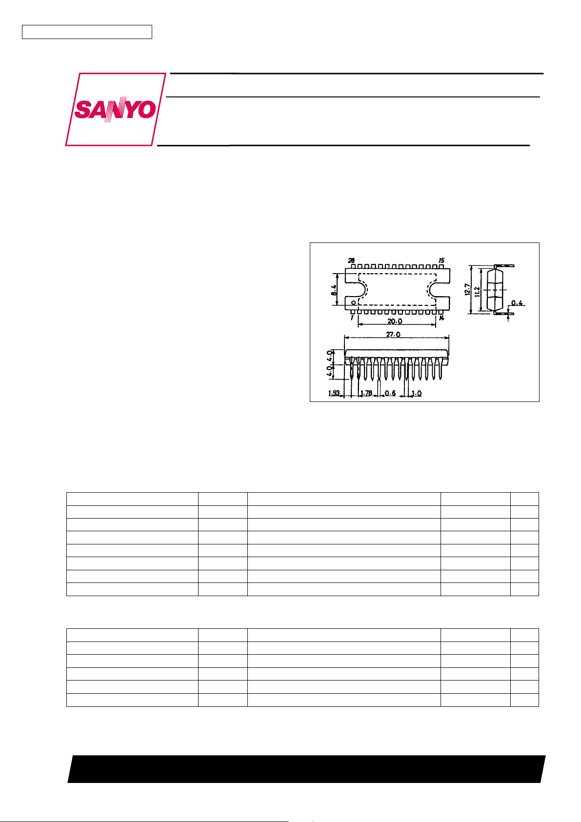
3147-DIP28HS
[LB1820]
SANYO : DIP28HS
Absolute Maximum Ratings atTa=25°C
Parameter Symbol Conditions Ratings Unit
Maximum supply voltage 1 V
Maximum supply voltage 2 V
Output current I
Allowable power dissipation 1 Pd max 1 Independent IC 3 W
Allowable power dissipation 2 Pd max 2 With arbitrarily large heat sink 20 W
Operating temperature Topr –20 to +80
Storage temperature Tstg –55 to +150
CC
O
M
t % 100 ms 2.5 A
30 V
30 V
Allowable Operating Ranges atTa=25°C
Parameter Symbol Conditions Ratings Unit
Supply voltage range 1 V
Supply voltage range 2 V
Voltage regulator output current I
Comparator output current I
Lock detector output current I
CC
M
VH
OSC
LD
9.5 to 28 V
5to28 V
0 to +20 mA
0 to +30 mA
0 to +20 mA
C
°
C
°
SANYO Electric Co.,Ltd. Semiconductor Bussiness Headquarters
TOKYO OFFICE Tokyo Bldg., 1-10, 1 Chome, Ueno, Taito-ku, TOKYO, 110 JAPAN
43096HA(II)/3260TA, TS(GTPS) No.3302-1/7
Page 2
LB1820
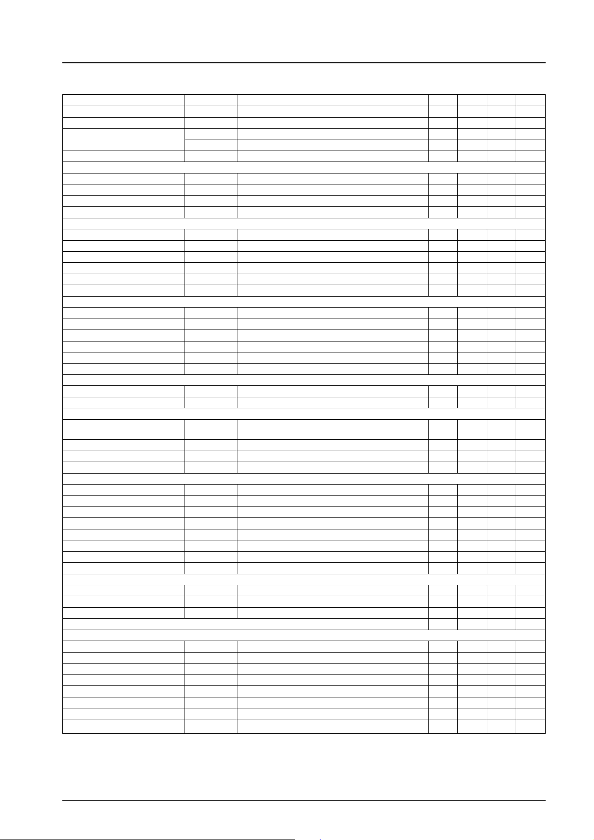
Electrical Characteristics atTa=25°C, VCC=VM=24V
Parameter Symbol
Supply current 1 I
Supply current 2 I
Output saturation voltage
V
V
Output leak current I
CC1
CC2
O (sat)
O(sat)
leak 100 µA
O
Stop mode 3 5 mA
1IO= 1 A 2.1 3.0 V
2IO= 2 A 3.0 4.2 V
Conditions
min typ max Unit
33 50 mA
Voltage regulator
Output voltage V
Voltage variation ∆V
Load variation ∆V
IVH= 10 mA 3.8 4.15 4.5 V
H
1VCC= 9.5 to 28 V 60 150 mV
H
2IVH=5to20mA 60 150 mV
H
Temperature coefficient –2 mV/°C
Hall amp
Input bias current I
Common-mode input voltage V
HB
ICM
1.5 2.8 V
14µA
Hall input sensitivity 100 mVp-p
Hysteresis width ∆V
Low-to-high input voltage V
High-to-low input voltage V
IN
SLH
SHL
24 33 42 mV
82032mV
–25 –13 –1 mV
Oscillator
High-level output voltage V
Low-level output voltage V
OH(CR)
OL(CR)
2.9 3.2 3.5 V
0.9 1.1 1.3 V
Oscillation amplitude 1.8 2.1 2.4 V
Oscillation frequency f R = 30 kΩ, C = 1500 pF 18.5 kHz
Temperature coefficient ∆f 0.1 %/°C
Comparator output voltage V
OSC
I
= 20 mA 1.5 V
OSC
Current limiter
Limiter 1 V
Limiter 2 V
1 0.42 0.5 0.6 V
Rf
2 0.4 0.44 0.48 V
Rf
Thermal shutdown
Thermal shutdown
temperature
TSD Design target 150 180
Hysteresis width ∆TSD 30
Low-voltage protection voltage V
Hysteresis width ∆V
LVSD
LVSD
7.5 8.1 8.7 V
0.45 0.6 0.75 V
FG amp
Input offset voltage V
Input bias current I
High-level output voltage V
Low-level output voltage V
IO(FG)
B(FG)
OH(FG)IFG
OL(FG)I(FG)
= –2 mA 5.6 6.2 6.8 V
= 2 mA 1 1.5 V
–10 +10 mV
–1 +1 µA
FG input sensitivity 10 × Gain 5 mV
Schmitt width at next stage 16 mV
Operating frequency range 5 kHz
Open-loop voltage gain 60 dB
Speed discriminator
High-level output voltage V
Low-level output voltage V
OH(D)
OL(D)
4.7 V
0.3 V
Maximum clock frequency 1.0 MHz
Number of counts 2044 2046 2048
Integrator
Input offset voltage V
Input bias current I
High-level output voltage V
Low-level output voltage V
IO(INT)
B(INT)
OH(INT)
OL(INT)
–10 +10 mV
–0.4 +0.4 µA
3.7 4.3 4.9 V
0.8 1.2 V
Open-loop gain 60 dB
Gain-bandwidth product 1.6 MHz
Reference voltage –5% V5/2 5% V
5 V supply V5 4.6 5 5.4 V
C
°
C
°
Continued on next page.
No.3302-2/7
Page 3

Continued from preceding page.
LB1820
Parameter Symbol
Lock detector
Low-level output voltage V
Lock range ±3.125 %
Start/stop pin
Start/stop operating voltage 0.4 0.5 0.6 V
Crystal Oscillator
Precision of oscillating
frequency
Temperature coefficient –3
Drift in rotational speed ±0.01 %
OL(LD)ILD
=10 mA 0.5 V
Referenced to indicated frequency –500 +500 ppm
Conditions
min typ max Unit
ppm/°C
Truth Table
Source → Sink
1 OUT 3 → OUT 2 H H L
2 OUT 3 → OUT 1 H L L
3 OUT 2 → OUT 1 H L H
4 OUT 2 → OUT 3 L L H
5 OUT 1 → OUT 3 L H H
6 OUT 1 → OUT 2 L H L
Input
IN1 IN2 IN3
Pin Assignment
Allowable power dissipation, Pd max – W
Top view
With arbitrarily large
heat sink
Without heat sink
Ambient temperature, Ta –°C
No.3302-3/7
Page 4
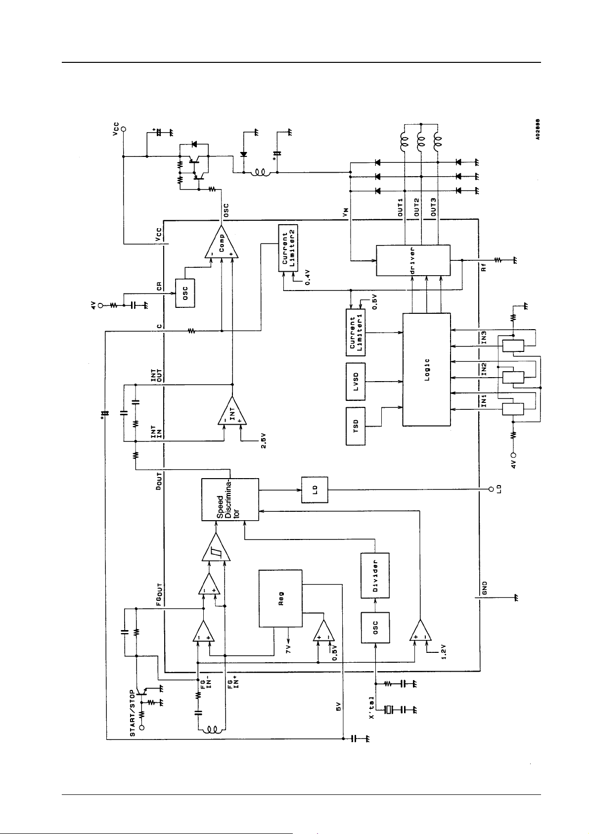
Internal Equivalent Circuit Block Diagram
LB1820
No.3302-4/7
Page 5
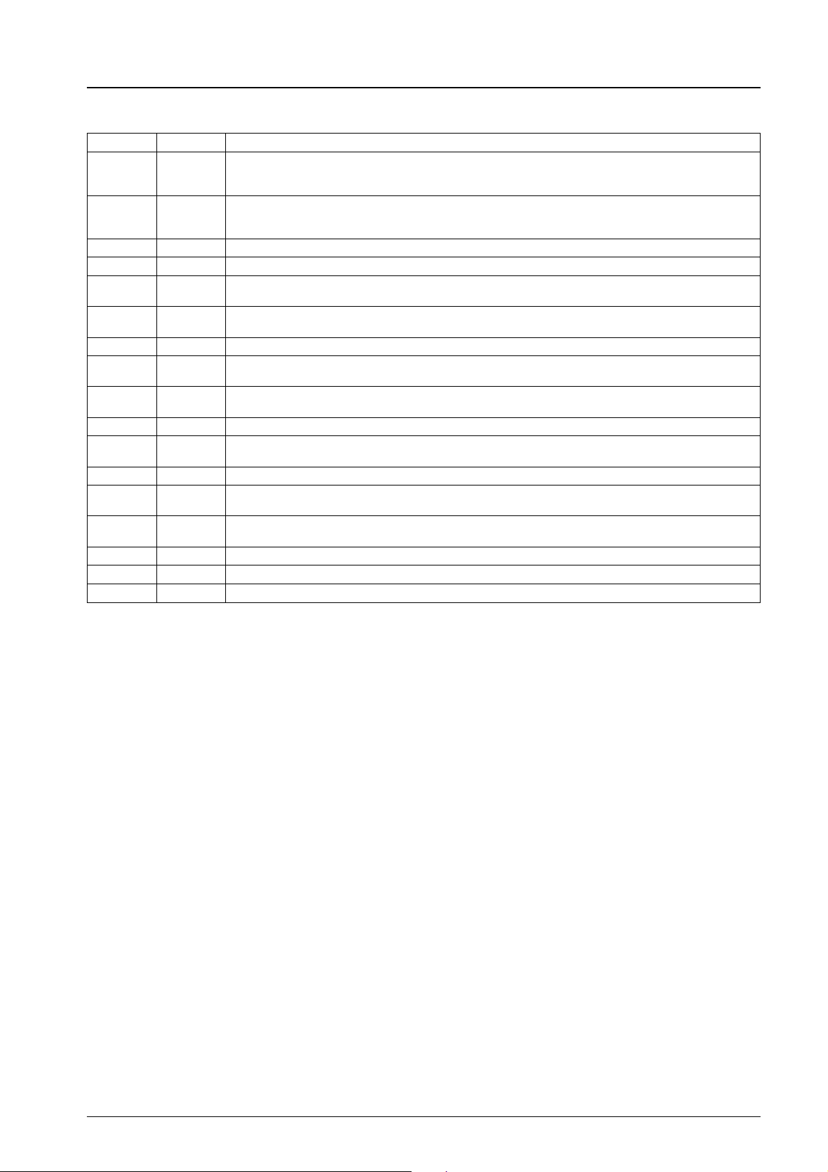
Pin Description
LB1820
Pin No. Pin Name Functions
19, 20
17, 18
15, 16
6
8
10
2V
12 V
11 R
+
IN
+
IN
+
IN
OUT 1
OUT 2
OUT 3
1, IN–1
2, IN–2
3, IN–3
CC
M
f
OUT 1: Hall element input pins for Phase 1. ‘‘H’’ logic is the state when IN
OUT 2: Hall element input pins for Phase 2. ‘‘H’’ logic is the state when IN
OUT 3: Hall element input pins for Phase 3. ‘‘H’’ logic is the state when IN
Output pin 1.
Output pin 2.
Output pin 3.
Power supply for other than output blocks.
Power supply for output blocks.
Output current detection pin. Rfis connected across this pin and GND to detect the output current as
voltage.
14 GND Ground for other than output blocks.
The lowest potential of output transistor is the voltage at R
f
pin.
3 CR Sets the oscillating frequency of the switching regulator.
1 OSC Outputs duty-controlled pulses.
Open-collector output.
24 INT
25 INT
23 D
OUT
Integrator output pin (speed control pin).
OUT
Varies the switching regulator output voltage.
Integrator input pin.
IN
Speed discriminator output pin.
Goes LOW when the specified speed is exceeded.
4 C Suppresses ripples in the motor current during operation of current limiter 2.
22 LD Lock detection pin.
Goes HIGH when the motor rotation speed is within the locking range.
27
26
28 FG
FG
FG
IN
IN
OUT
–
FG pulse input (Start/Stop control) pin.
+
FG pulse input (4 V supply) pin.
FG amp output pin.
21 Xtal Crystal oscillator connecting pin.
13 5 V 5 V supply pin.
+
>IN−.
+
>IN−.
+
>IN–.
No.3302-5/7
Page 6

LB1820
Operation Notes
Speed Control Circuit
This IC uses a speed discrimination circuit to perform speed control. The rotation accuracy of the speed discrimination method
depends on the counter count. The counter count in this IC is 2046. On the FG1 cycle, a speed error signal with a resolution of
1/2046 is output from the D
The D
output shifts among three states: high, high impedance, and low:
OUT
High : Output S (acceleration signal)
High impedance : When neither output S nor output F is output
Low : Output F (deceleration signal)
The relationship between the FG frequency (f
f
FG=fOSC
÷ (ECL division ratio × count)
÷ (8 × 2046)
f
OSC
÷ 16368
f
OSC
PAM Drive System
This IC controls motor rotations by configuring an external switching regulator, and controlling the voltage (VM) of the regulator.
Select a switching regulator diode with a short reverse recovery time such as an FRD (First Recovery Diode). Because even a
smooth coil can become a noise source, attention must be paid to the arrangement of components on the board (especially
avoiding the effects of FG signal lines and integrated amplifiers).
Select a normal rectifier diode for the upper and lower motor drive pin section (OUT1 to 3).
pin (charge pump method).
OUT
FG
) and the quartz oscillation frequency (f
) can be calculated as follows:
OSC
Current Limiter Circuit
The current limiter circuit consists of two limiter circuits.
1 Limiter 1
Detection voltage V
1 = 0.5 V typ. Current is limited by putting the lower output transistor in the nonsaturated state and
Rf
then dropping the voltage applied to the motor.
2 Limiter 2
Detection voltage V
2 = 0.44 V typ. The VMvoltage is limited by limiting the OSC pin ‘‘on duty’’ ratio.
Rf
Normally, if an excessive load is put on the motor, limiter 1 operates first, and after a delay in the switching regulator, limiter 2
operates.
Sometimes, after startup, the ASO of the output transistor is very severe. In such a case, it is necessary to perform a soft start (in
which V
is increased gradually). When using soft starts, connect a capacitor between the pin (VM, 5 V, etc.) on which the
M
voltage is to be increased during startup and the C pin. If soft starts are not to be used, connect a capacitor between the C pin and
ground.
Speed Lock Range
The speed lock signal is output from the LD pin. The speed lock range is within ±3.13%; if the motor rotations fall within the
lock range the LD pin goes low (open collector output).
Start/stop Operation
The FG
−
pin also serves as the start/stop pin. When the FG
IN
or less, the stop state goes into effect. In the stopped state, in addition to the drive outputs being turned off, the FG
other regulator outputs are also turned off.
When it is necessary to drive the motor at high speed, improvement is possible by adding a resistor (of approximately 1 MΩ)
between FG
and VCC. (The time from when the transistor is turned off until FG
OUT
−
pin is connected to a transistor, etc., and the voltage is 0.5 V typ.
IN
−
goes to 0.5V is reduced.)
IN
+
, 5 V, and
IN
Initial Reset Operation
At startup, it is possible to apply an initial reset to the logic circuits by delaying the increase in voltage on FG
reset is not applied, the LD pin may go low from start until the FG pulse is input to the logic circuits (until output of
approximately 16 mVp-p is generated on FG
When an FG reset is applied, the capacitor between the FG
−
FG
). Caution is required, because if the FG amplifier input capacitor is too small and the feedback capacitor is too large, the
IN
OUT
).
+
and GND should be 4.7 µF or more (in order to delay the rise in
IN
reset time will be shorter. At start, a delay of about 5 µs or more from the rising edge of the 5 V regulator output until the FG
voltage goes to 1.2 V is desirable.
−
. If an initial
IN
No.3302-6/7
−
IN
Page 7
LB1820
PWM Frequency Setting
The PWM frequency is determined by the resistor and capacitor connected to the CR pin. When a resistor is connected to the
FG
pin, the PWM frequency can be roughly calculated by the following formula:
IN+
f
6 1 ÷ (1.2 × C × R)
PWM
The resistor must not be less than 30 kΩ. It is desirable for the PWM frequency to be about 15 kHz.
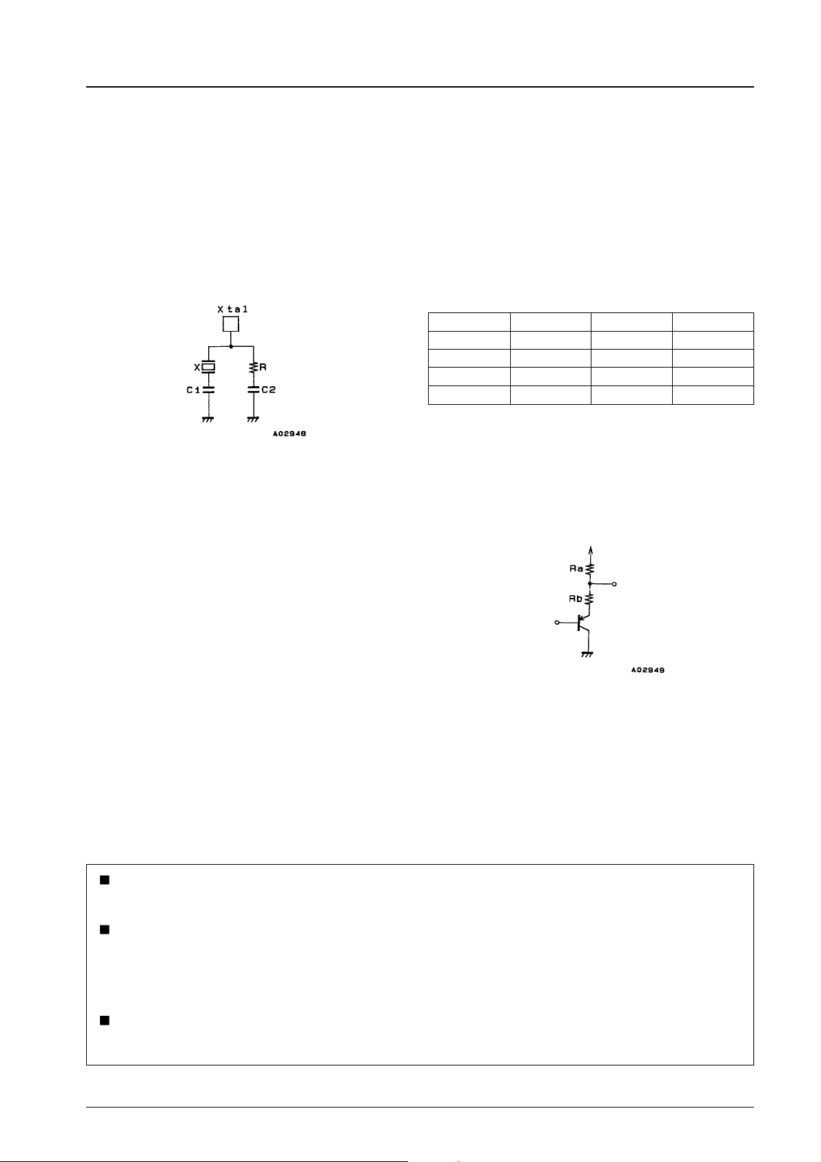
Quartz Oscillator
An oscillator, capacitor and resistor are to be connected to the quartz oscillator. When selecting the oscillator and the external
capacitor and resistor, always obtain approval from the manufacturer of the oscillator in order to avoid problems.
(Circuit with external quartz oscillator)
External constants (reference values)
Xtal (MHz) C1 (pF) C2 (pF) R (kΩ)
3 to 4 39 82 0.82
4 to 5 39 82 1.0
5 to 7 39 47 1.5
7to10 39 27 2.0
However, use a crystal such that the base wave
impedance : 3fOimpedance=1:5ormore
f
O
When inputting external signals (of several MHz) to the quartz oscillator, connect external components as shown in the diagram
below.
5 V pin
=1to8MHz
f
IN
Input signal level High level voltage: 4.0 V min.
Low level voltage: 1.5 V max.
Ra=2kΩ,Rb=1kΩ(reference values)
Xtal pin
Input
No products described or contained herein areintendedforuse in surgical implants, life-support systems, aerospace equipment,
nuclear power control systems, vehicles, disaster/crime-prevention equipment and the like, the failure of which may directly or
indirectly cause injury, death or property loss.
Anyone purchasing any products described or contained herein for an above-mentioned use shall:
1 Accept full responsibility and indemnify and defend SANYO ELECTRIC CO., LTD., its affiliates, subsidiaries and distributors
and all their officers and employees, jointly and severally, against any and all claims and litigation and all damages, cost and
expenses associated with such use:
2 Not impose any responsibility for any fault or negligence which may be cited in any such claim or litigation on SANYO
ELECTRIC CO., LTD., its affiliates, subsidiaries and distributors or any of their officers and employees jointly or severally.
Information (including circuit diagrams and circuit parameters) herein is for example only; it is not guaranteed for volume
production. SANYO believes information herein is accurate and reliable, but no guarantees are made or implied regarding its use
or any infringements of intellectual property rights or other rights of third parties.
This catalog provides information as of April, 1996. Specifications and information herein are subject to change without notice.
No.3302-7/7
 Loading...