

Page 1
Ordering number :EN5452
73097HA (OT) No. 5452-1/7
Functions
• The LB1955 is a 3-phase brushless motor driver IC that
is optimal for applications such as driving the drum
motor in VCRs.
Features
• Current linear drive
• FG and PG free
• Single-voltage power supply
• Built-in AGC circuit
• Built-in thermal shutdown circuit
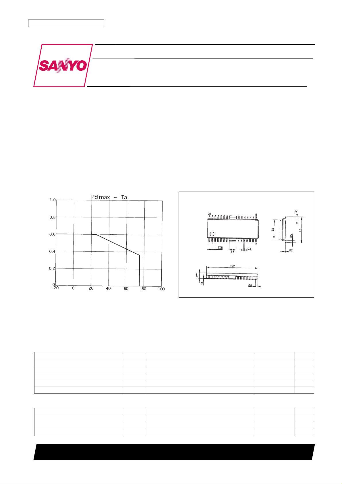
Package Dimensions
unit: mm
3222-HSOP28
SANYO: HSOP28
[LB1955]
SANYO Electric Co.,Ltd. Semiconductor Bussiness Headquarters
TOKYO OFFICE Tokyo Bldg., 1-10, 1 Chome, Ueno, Taito-ku, TOKYO, 110 JAPAN
Monolithic Digital IC
LB1955
Three-Phase Brushless Motor Driver
Parameter Symbol Conditions Ratings Unit
Maximum supply voltage V
CC
max 14.5 V
Maximum output current I
OUT
1.0 A
Allowable power dissipation Pdmax Independent device 0.60 W
Operating temperature Topr –20 to +75 °C
Storage temperature Tstg –55 to +150 °C
Specifications
Absolute Maximum Ratings at Ta = 25°C
Parameter Symbol Conditions Ratings Unit
Supply voltage V
CC
10.2 to 13.8 V
Hall input amplitude Vhall At the input 70 to 500 mVp-p
VC input voltage V
C
0 to 5 V
Allowable Operating Ranges at Ta = 25°C
Ambient temperature, Ta – °C
Allowable power dissipation, Pd max – W
Page 2
No. 5452-2/7
LB1955
Electrical Characteristics at Ta = 25°C, VCC= 12 V
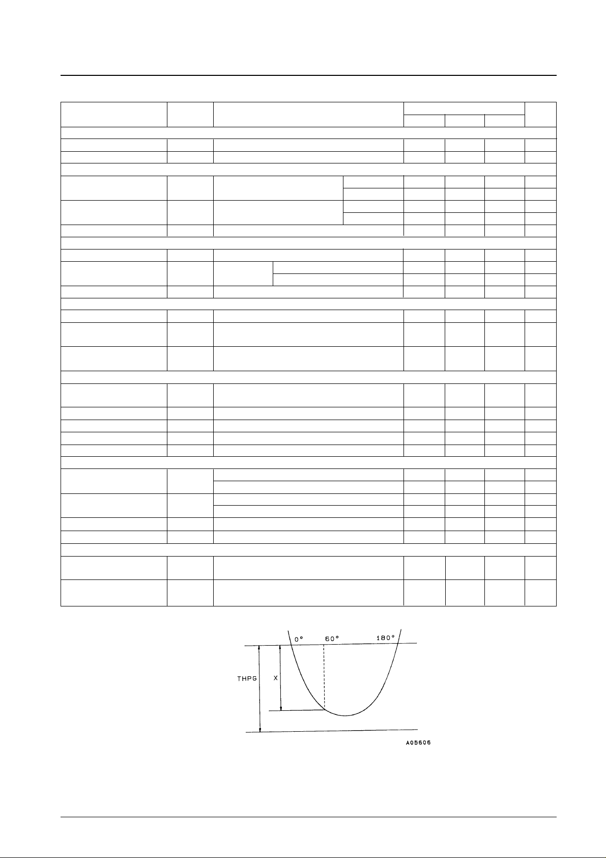
Note: * is provided for when X is the peak value at the 60° position of the lower side of the UIN1 Hall amplifier input: THPG = 1.17X.
Parameter Symbol Conditions
Ratings
Unit
min typ max
[Power Supply]
Current drain I
CC
VC= 0 V, LCTR = 6 V 7.0 10.0 13.0 mA
IC internal power supply V
REF
4.75 5.0 5.25 V
[Output]
Output saturation voltage V
O(sat)
1
I
O
= 400 mA Sink side 0.4 V
V
C
= 5 V, Rf= 0 Ω Source side 1.5 V
Output saturation voltage 2 V
O(sat)
2
I
O
= 800 mA Sink side 0.7 V
V
C
= 5 V, Rf= 0 Ω Source side 2.0 V
3-phase output current ripple Ior I
O
= 100 mA, Rf = 0.47 Ω –5 +5 %
[Hall Amplifier]
Input offset voltage VHoff –20 +20 mV
Input bias current IHb
V
AGC
= 1.4 V
U
IN
10 µA
V
IN
, W
IN
5 µA
Common-mode input voltage range
V
HCM
2.2 5.0 V
[Control]
VC pin input bias current I
VCb
VC= 0 V –10 –1.3 µA
Control start voltage V
THVC
Rf= 0.47 Ω, IO≥ 10 mA
2.25 2.5 2.75 V
With the Hall input logic fixed
Open-loop control gain G
MVC
Rf= 0.47 Ω, ∆IO= 200 mA
0.72 0.9 1.08 A/V
With the Hall input logic fixed and VG shorted to RF
[PG]
PG Hall amplifier
V
PGoff
Design target –10 +10 mV
input offset voltage
Peak hold charge current I
SHCHG
(U, V, W) = (L, L, H) 30 µA
PG comparator threshold THPG Design target* 117 %
PG output high-level voltage V
PGH
4.5 5.2 V
PG leakage current I
LEAKPG
–10 0 +10 µA
[FG]
Back emf Schmitt input
V
SCHG
In the back emf Schmitt input increasing direction, Design target 100 mV
hysteresis width
In the back emf Schmitt input decreasing direction, Design target 0 mV
Ringing canceller Schmitt
V
SCHR
In the Schmitt input increasing direction, Design target 180 mV
input hysteresis width
In the Schmitt input decreasing direction, Design target –20 0 +20 mV
FG output high-level voltage V
FGH
FGR = 0 V 4.5 5.2 V
FG leakage current I
LEAKFG
–10 0 +10 µA
[TSD]
Thermal shutdown
TTSD Design target 180 °C
operating temperature
Thermal shutdown
∆TSD Design target 15 °C
temperature hysteresis width
Page 3
No. 5452-3/7
LB1955
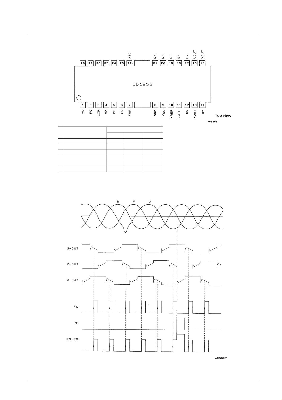
Pin Assignment
Source → sink
Hall input logic
U V W
1 W phase → V phase H H L
2 W phase → U phase H L L
3 V phase → U phase H L H
4 V phase → W phase L L H
5 U phase → W phase L H H
6 U phase → V phase L H L
Truth table
Note: The Hall input "H" and "L" values are defined as follows: "H" means that for that phase the (+) input is higher than the (-) input, and "L" means that for
that phase the (+) input is lower than the (-) input. However, note that an input potential difference corresponding to the Hall to output gain is required.
Timing Charts
Note: The Hall inputs are defined as follows: U = UIN1 – UIN2, V = VIN1 – VIN2, and W = WIN1 – WIN2.
Inputs to the Hall input pins must be applied in the phase order shown in the timing chart.
Hall inputs
Synthesized
waveform
W
IN
2
W
IN
1
V
IN
2
V
IN
1
U
IN
2
U
IN
1
Page 4
No. 5452-4/7
LB1955
Pin Functions
Pin No. Pin Function
23, 24 U
IN
1, UIN2 U phase Hall element input
25, 26 V
IN
1, VIN2 V phase Hall element input
27, 28 W
IN
1, WIN2 W phase Hall element input
16 UOUT U phase output
15 VOUT V phase output
13 WOUT W phase output
11 LCTR Pin connected to the center points of the coils that are Y-connected to the U, V, and W outputs.
9 V
CC
Power supply
10 V
REF
Reference voltage output
8 GND GND
14 Rf Output current detection
1 VG Closed loop control gain switching
2 FC Speed control loop frequency characteristics correction
3 LIM Output current limit setting
4 VC Speed control
5 PG PG waveform output
6 FG FG waveform output (FGR shorted to GND)
7 FGR PG/FG synthesized output (FGR shorted to PG)
18 SH PG waveform sample-and-hold circuit capacitor connection
22 AGC Connection for the capacitor used by the AGC circuit, which holds the input gain at a fixed level.
12, 17, 19
NC No connection
20, 21
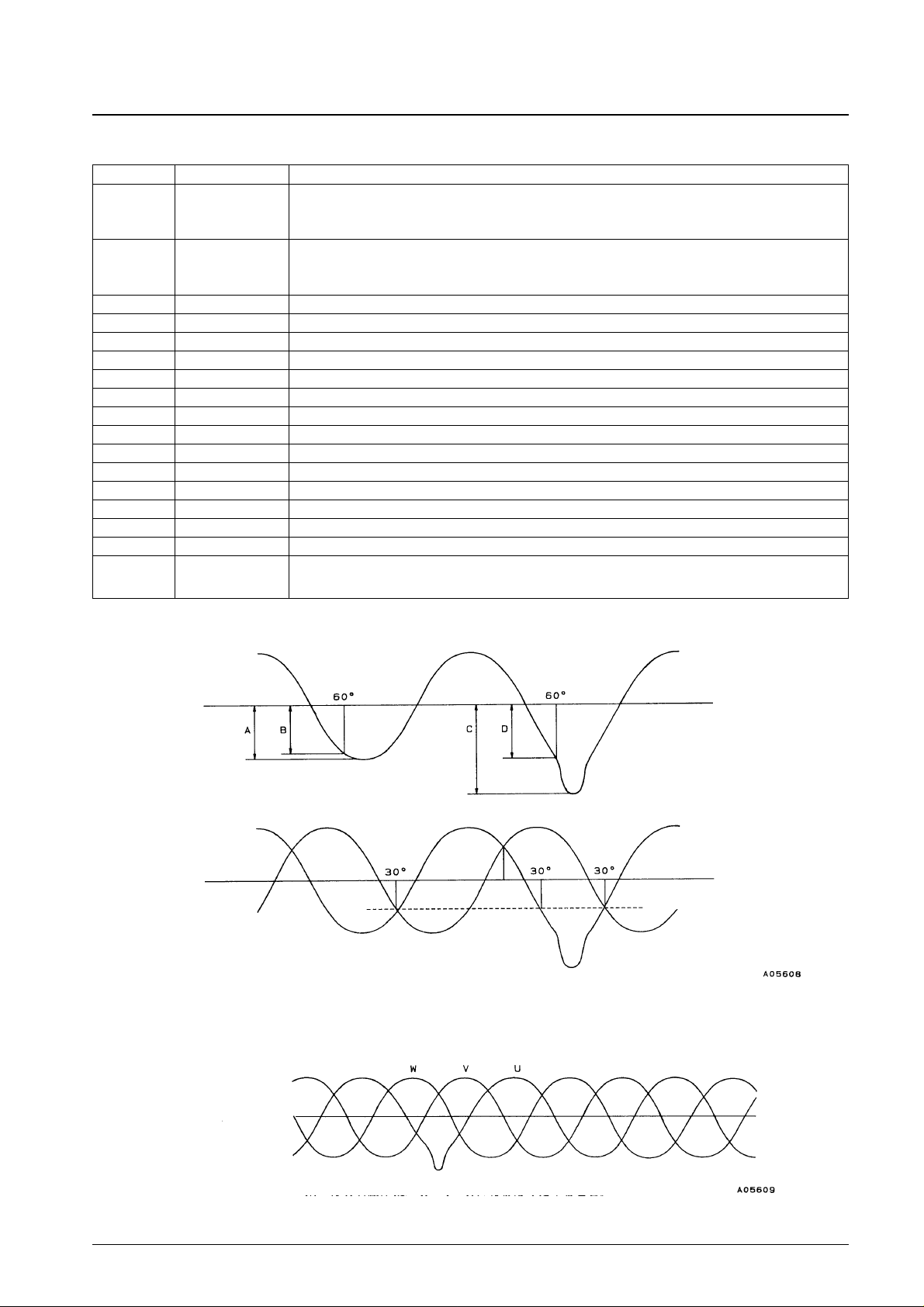
Recommended Special Magnetization Waveforms
Note: Note that the intersections between the special magnetization and general waveforms and the intersections between pairs of general waveforms must
be set up to be 30° apart.
Hall Input Order
Note: The Hall input order must be set up to be W → V → U.
B ≤ A < 7/6 × B
8/6 × D ≤ C ≤ 10/6 × D
Hall input
Page 5
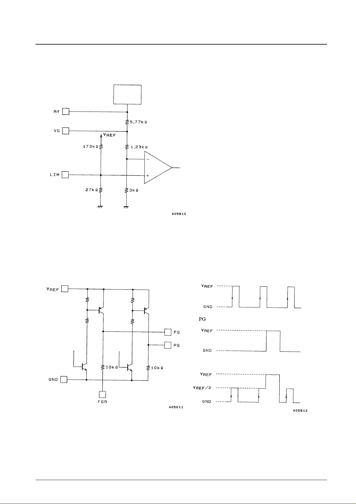
VG and LIM Pin Usage
No. 5452-5/7
LB1955
LIM pin: Open
VG – Rf: Shorted
Gm = 0.423/Rf (A/V)
(Closed loop control gain)
Ilim = (V
REF
× 27/200 – 0.2) × 4.23/3/Rf
(Current limit)
VG pin: Open
Gm = 1/Rf (A/V)
(Closed loop control gain)
Ilim = (V
REF
×27/200 – 0.2) ×10/3/Rf
(Current limit)
LIM – V
REF
: Shorted
No current limit.
Note: This current limiting function is for protection against unusual and abnormal currents. If a current limit level below the rated current is set, this will,
inversely, result in heat generation within the IC.
When the LIM pin is open, VG is shorted to Rf, and Rf = 0.47 Ω, this will result in a current limit level of about 1.3 to 1.4 A. If this limit falls under the
rated value due to mode changes or changes in the value of the Rf resistor, set the current limit to an appropriate value by applying to the LIM pin a
voltage that is divided from the V
REF
to ground potential by resistors of a few kΩ. Alternatively, short the LIM pin to V
REF
to defeat the current limit
function.
Output
stage
PG and FG Pin Output Circuits FG (FGR shorted to ground)
PG (FGR shorted to PG)
Page 6
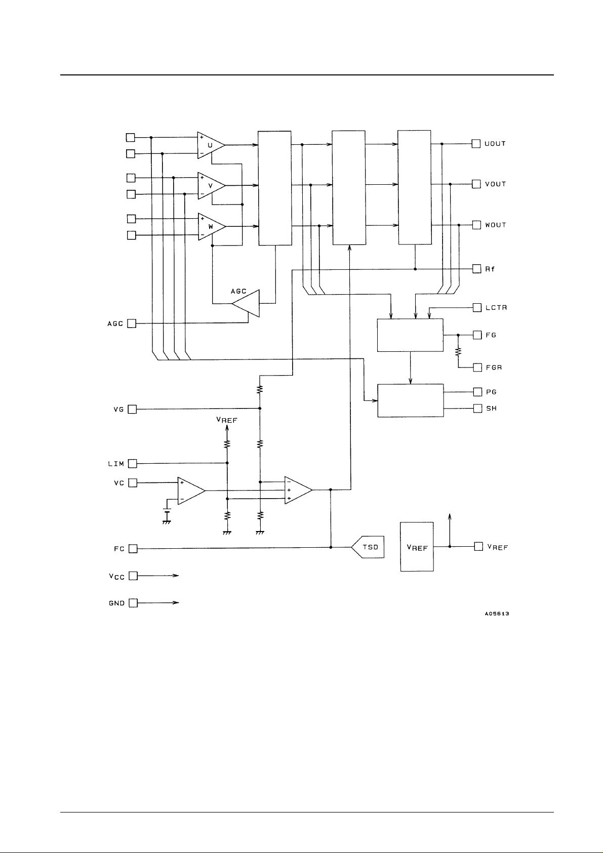
Block Diagram
No. 5452-6/7
LB1955
Hall input synthesis block
(linear matrix)
3-phase differential
distribution circuit
Power transistors
FG waveform
synthesis
PG waveform
synthesis
Internal power supply
UIN1
UIN2
VIN1
VIN2
WIN1
WIN2
Page 7
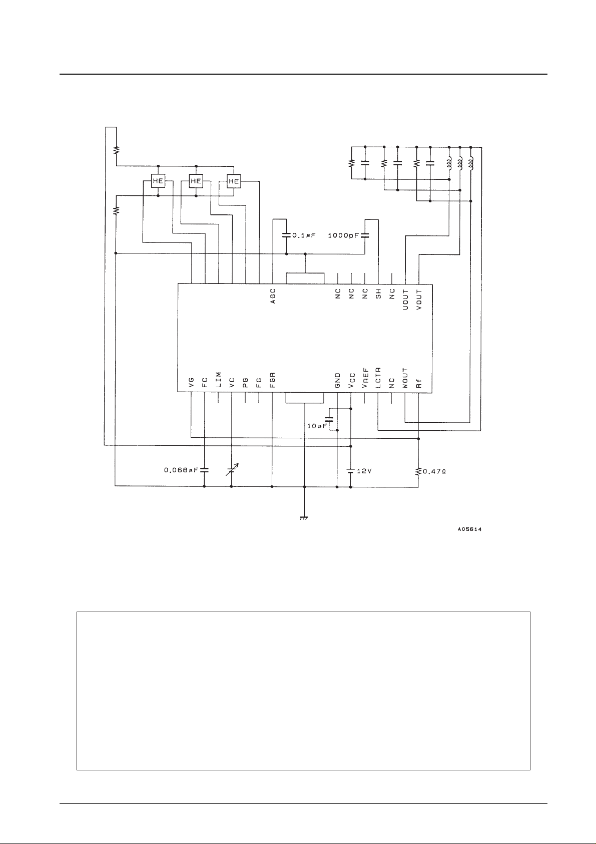
No. 5452-7/7
LB1955
Sample Application Circuit
This catalog provides information as of July, 1997. Specifications and information herein are subject to change
without notice.
■ No products described or contained herein are intended for use in surgical implants, life-support systems, aerospace
equipment, nuclear power control systems, vehicles, disaster/crime-prevention equipment and the like, the failure of
which may directly or indirectly cause injury, death or property loss.
■ Anyone purchasing any products described or contained herein for an above-mentioned use shall:
➀ Accept full responsibility and indemnify and defend SANYO ELECTRIC CO., LTD., its affiliates, subsidiaries and
distributors and all their officers and employees, jointly and severally, against any and all claims and litigation and all
damages, cost and expenses associated with such use:
➁ Not impose any responsibility for any fault or negligence which may be cited in any such claim or litigation on
SANYO ELECTRIC CO., LTD., its affiliates, subsidiaries and distributors or any of their officers and employees
jointly or severally.
■ Information (including circuit diagrams and circuit parameters) herein is for example only; it is not guaranteed for
volume production. SANYO believes information herein is accurate and reliable, but no guarantees are made or implied
regarding its use or any infringements of intellectual property rights or other rights of third parties.
LB1955
U
IN
1
U
IN
2
V
IN
2
V
IN
1
W
IN
1
W
IN
2
0 to 5 V
 Loading...