

Page 1

Overview
The LB1943 is a forward/reverse motor driver IC. This IC
supports forward, reverse, and braking control from a
single input, and the desired output voltage can be set with
a resistor. Either full drive or VC drive can be selected
from the single input, and the LB1943 can be controlled
from a microprocessor.
Functions
• Single-input control of forward, reverse, and braking
operations
• Resistor output voltage setup
• Either full drive or VC drive can be selected from the
single control input.
• Can be controlled from a microprocessor.
• Built-in motor dash current absorbing device
• Built-in reference voltage circuit
• Built-in thermal protection circuit
Package Dimensions
unit: mm
3043A-SIP10
Monolithic Digital IC
22898HA (OT) No. 5806-1/5
SANYO: SIP10
[LB1943]
SANYO Electric Co.,Ltd. Semiconductor Bussiness Headquarters
TOKYO OFFICE Tokyo Bldg., 1-10, 1 Chome, Ueno, Taito-ku, TOKYO, 110-0005 JAPAN
Forward/Reverse Motor Driver with Braking Function
LB1943
Ordering number : EN5806
Parameter Symbol Conditions Ratings Unit
Maximum supply voltage V
CC
max 18 V
Input voltage V
IN
VCC≥ V
IN
–0.3 to +6 V
Output current I
OUT
±1.6 A
Allowable power dissipation Pd max 1.2 W
Operating temperature Topr –25 to +75 °C
Storage temperature Tstg –55 to +125 °C
Specifications
Absolute Maximum Ratings at Ta = 25°C
Parameter Symbol Conditions Ratings Unit
Supply voltage range
V
CC
1 8 to 18 V
V
CC
2VCC1 ≥ VCC2 5 to 18 V
Forward-reverse disabled time Toff Over 20 µs
Allowable Operating Ranges at Ta = 25°C
Parameter Symbol Conditions
Ratings
Unit
min typ max
Input low-level voltage V
INL
01V
Input high-level voltage V
INH
4.2 6.0 V
Input mid-level voltage V
INM
23V
Input impedance Z
IN
75 kΩ
Current drain I
CC
5.5 10.0 mA
Electrical Characteristics at Ta = 25°C, VCC= 12 V
Continued on next page.
Page 2
No. 58062/5
LB1943
Continued from preceding page.
Note: Items marked with an asterisk (*) are design target values, and are not tested.
Input levels: VH: Over 4.2 V
V
M
: 2.0 to 3.0 V
V
L
: Under 1.0 V
IN1 and IN2 go to 2.5 V when left open.
LB1943 operation is equivalent to that of the LB1641.
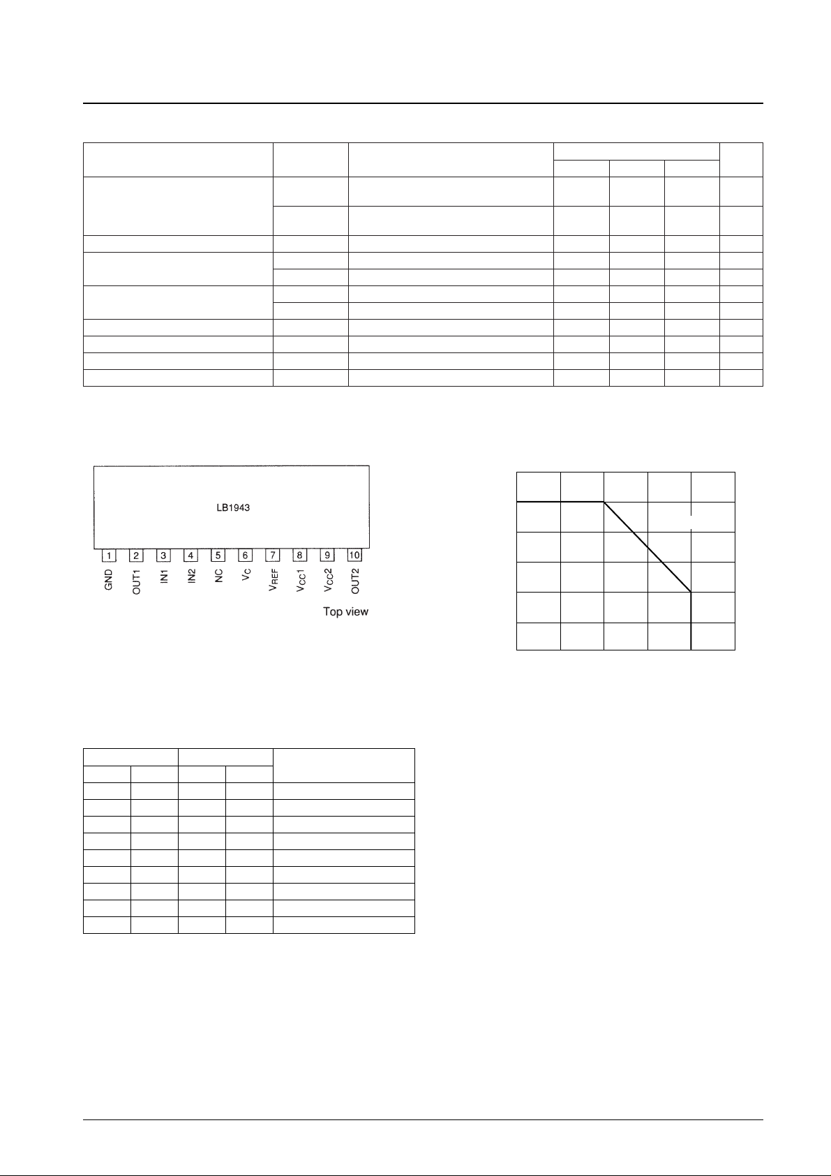
Pin Assignment
Parameter Symbol Conditions
Ratings
Unit
min typ max
V
OUT
1
R
L
= 60 Ω, VC= 2.5 V
4.4 4.95 5.4 V
Output voltage
V
IN
1 = 2.5 V, VIN2 = 0 V
V
OUT
2
R
L
= 60 Ω, VC= 2.5 V
4.4 4.95 5.4 V
V
IN
1 = 2.5 V, VIN2 = 5.0 V
Output leakage current I
OL
RL= ∞ 0.01 1.0 mA
Saturation voltage (upper)
V (sat)11 V
CC
= 12V, I
OUT
= 300 mA 1.9 2.2 V
V (sat)12 V
CC
= 12V, I
OUT
= 500 mA 1.9 2.3 V
Saturation voltage (lower)
V (sat)21 V
CC
= 12V, I
OUT
= 300 mA 0.25 0.5 V
V (sat)22 V
CC
= 12V, I
OUT
= 500 mA 0.4 0.65 V
Reference power supply V
REF
6.0 6.35 6.8 V
Reference voltage load characteristics ∆V
REF
/∆I
REFIREF
= 0 to –2.0 mA 0.05 0.1 V/mA
Control-to-output gain V
OUT/VC
, VC= 2.5 V, RL= 60 Ω 1.5 1.9 2.4 ×
TSD operating temperature T
STD
* 150 180 °C
Truth Table
Input Output voltage
Operation
IN1 IN2 OUT1 OUT2
H H L FULL Forward (reverse) operation
M H L V
C
× 2 Forward (reverse) operation
L H L V
C
× 2 Forward (reverse) operation
H M OFF OFF Braking
M M OFF OFF Braking
L M OFF OFF Braking
H L FULL L Reverse (forward) operation
M L V
C
× 2 L Reverse (forward) operation
L L V
C
× 2 L Reverse (forward) operation
1.4
1.2
1.0
0.8
0.6
Pd max – Ta
Tj = 125 °C
0.6
0.4
0
Allowable power dissipation, Pd max – W
-25
0 25 50 75 100
Ambient temperature, Ta – °C
Page 3
No. 58063/5
LB1943
Pin No. Symbol Pin function Equivalent circuit
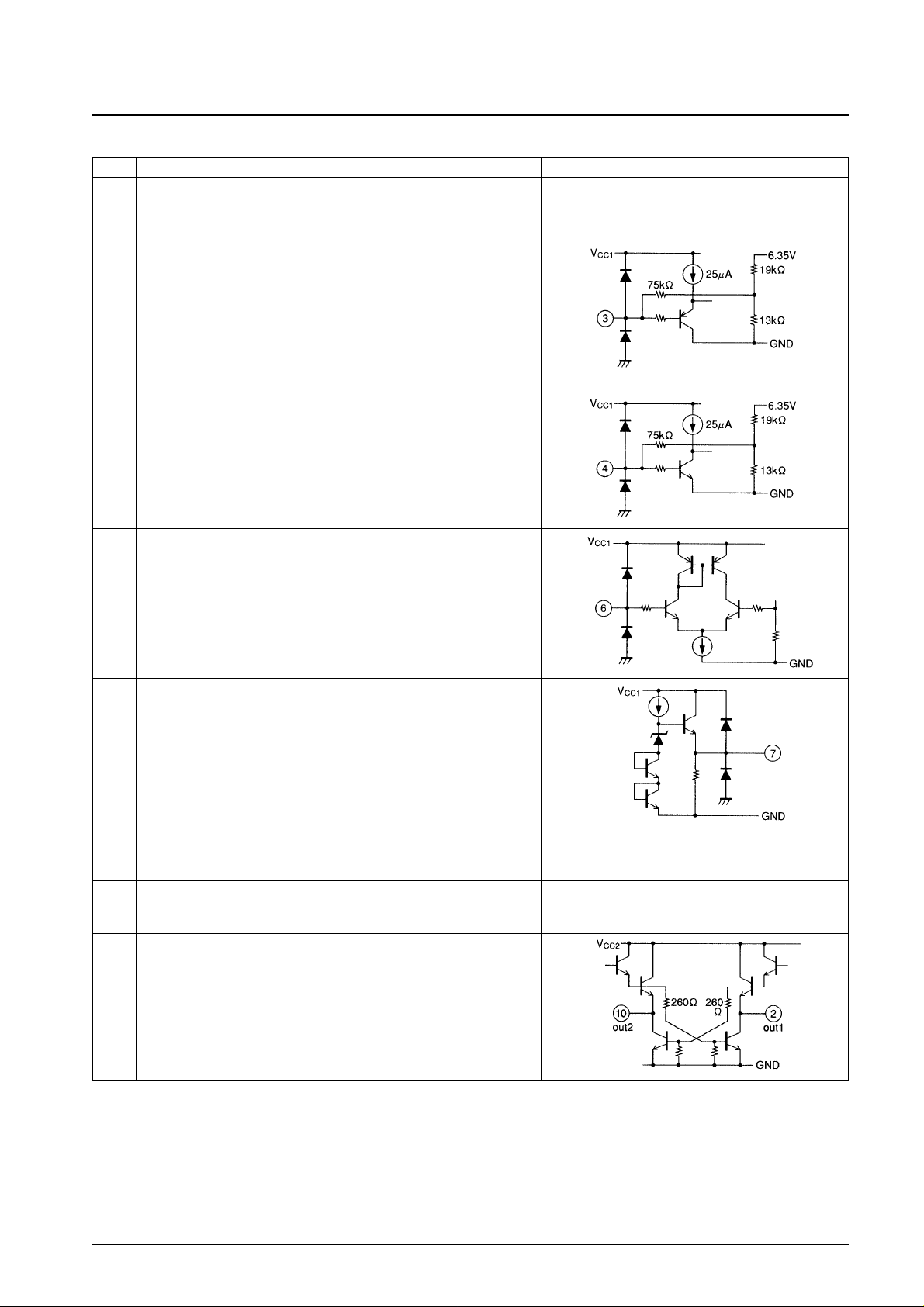
Pin Functions
1 GND
• Power system ground. This line is shared with the signal system
ground.
3 IN1
• Output voltage switching input
• Goes to V
M
(about 2.5 V) when left open.
4 IN2
• Forward, reverse, or braking control input
• Goes to V
M
(about 2.5 V) when left open.
6
V
C
• Output voltage setting
7
V
REF
• Reference voltage output. V
REF
= 6.35 V
8
VCC1
• Signal system power supply
9
VCC2
• Power system power supply
2
10
OUT1
OUT2
• Outputs that are connected to the motor coils
Page 4
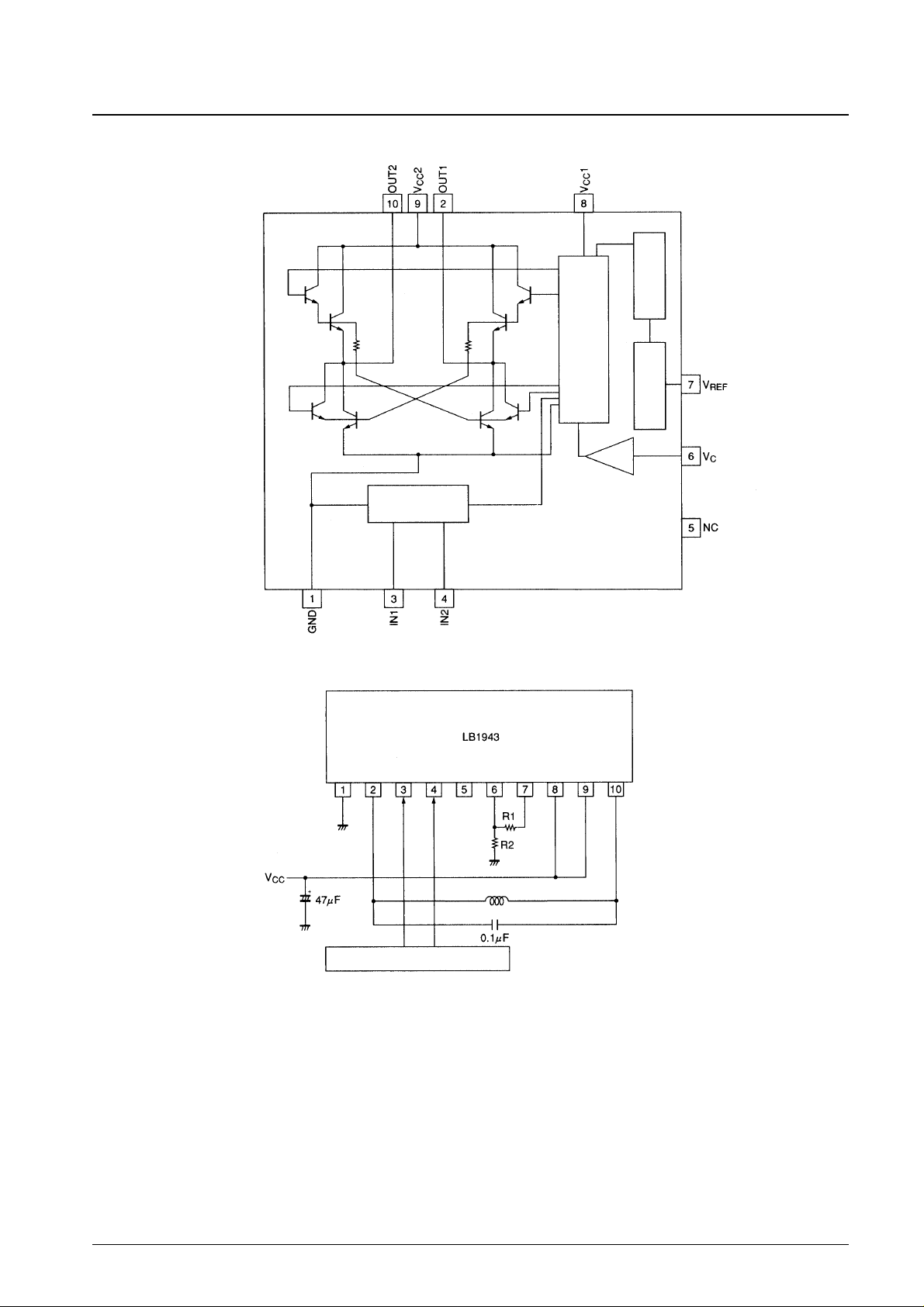
Internal Equivalent Circuit
No. 58064/5
LB1943
Peripheral Circuit Example
Usage Notes
1. The microprocessor output ports are CMOS outputs, and must be used in the high, low, or open states.
2. We recommend using a value of about 60 kΩfor R1 and R2.
3. Voltages applied to the IN1 and IN2 pins must not exceed the range 0 to 6 V. Note that negative voltages can cause
the IC to operate incorrectly. Also, do not apply voltages to IN1 or IN2 when the VCCvoltage is not applied.
4. To prevent the upper and lower output transistors from both being in the on state at the same time, when switching
the IN1 and IN2 values, always hold the input open for a brief period during the transition. We recommend holding
the open state for a few tens of microseconds.
5. A capacitor must be inserted between VCCand ground. We recommend that this capacitor have a value of at least
20 µF.
Microcontroller control port
Motor
Logic circuit
Pre-driver
Thermal
protection circuit
Reference
voltage circuit
Page 5

PS No. 5806-5/5
LB1943
6. During motor drive, large currents (on the order of several hundred mA) flow in the motor power supply block.
Therefore, the printed circuit board layout and interconnections must be designed so that there are no shared devices.
7. If negative voltages are applied to OUT1 and OUT2 and the IC operates incorrectly, insert Schottky diodes between
OUT1 and ground and between OUT2 and ground.
This catalog provides information as of February, 1998. Specifications and information herein are subject to
change without notice.
■ No products described or contained herein are intended for use in surgical implants, life-support systems, aerospace
equipment, nuclear power control systems, vehicles, disaster/crime-prevention equipment and the like, the failure of
which may directly or indirectly cause injury, death or property loss.
■ Anyone purchasing any products described or contained herein for an above-mentioned use shall:
➀ Accept full responsibility and indemnify and defend SANYO ELECTRIC CO., LTD., its affiliates, subsidiaries and
distributors and all their officers and employees, jointly and severally, against any and all claims and litigation and all
damages, cost and expenses associated with such use:
➁ Not impose any responsibility for any fault or negligence which may be cited in any such claim or litigation on
SANYO ELECTRIC CO., LTD., its affiliates, subsidiaries and distributors or any of their officers and employees
jointly or severally.
■ Information (including circuit diagrams and circuit parameters) herein is for example only; it is not guaranteed for
volume production. SANYO believes information herein is accurate and reliable, but no guarantees are made or implied
regarding its use or any infringements of intellectual property rights or other rights of third parties.
 Loading...