

Page 1
Ordering number : EN4179A
41596HA (OT) No. 4179-1/7
Overview
The LB1832V is a bidirectional driver IC that includes an
on-chip low-voltage low-saturation 1.5-channel bridge and
is provided in a miniature package. It is therefore optimal
for cameras that use 3 V lithium batteries. This IC allows
direct drive from the control microprocessor and supports
control of standby, forward, reverse, and braking
operations for two motors, i.e. the film take-up and lens
drive motors, from three inputs.
Features
• Supports low-voltage drive.
— When the same power supply is used for VCCand
VS: VCC= VS= 1.6 V min.
— When different power supplies are used for VCCand
VS: VS= 1.0 V min, VCC= 2.5 V min.
• Low saturation voltage (Upper side transistor plus lower
side transistor remaining voltage: 0.6 V (typ) at 1 A)
• Zero current drain in standby mode
• 1.5-channel bidirectional driver that can be directly
driven from the control microprocessor
• Separate logic and motor power supply connections
• Brake function
• Built-in spark killer diode
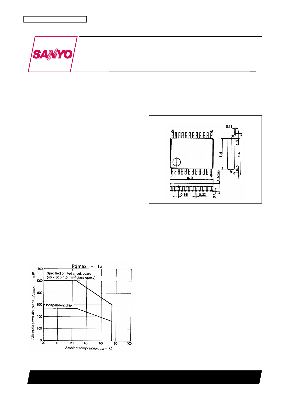
• Miniature package (SSOP-24)
Package Dimensions
unit: mm
3175A-SSOP24
SANYO: SSOP24
[LB1832V]
LB1832V
SANYO Electric Co.,Ltd. Semiconductor Bussiness Headquarters
TOKYO OFFICE Tokyo Bldg., 1-10, 1 Chome, Ueno, Taito-ku, TOKYO, 110-0005 JAPAN
Low-Saturation 1.5-Channel 3 V Drive
Bidirectional Driver
Monolithic Digital IC
Page 2
Specifications
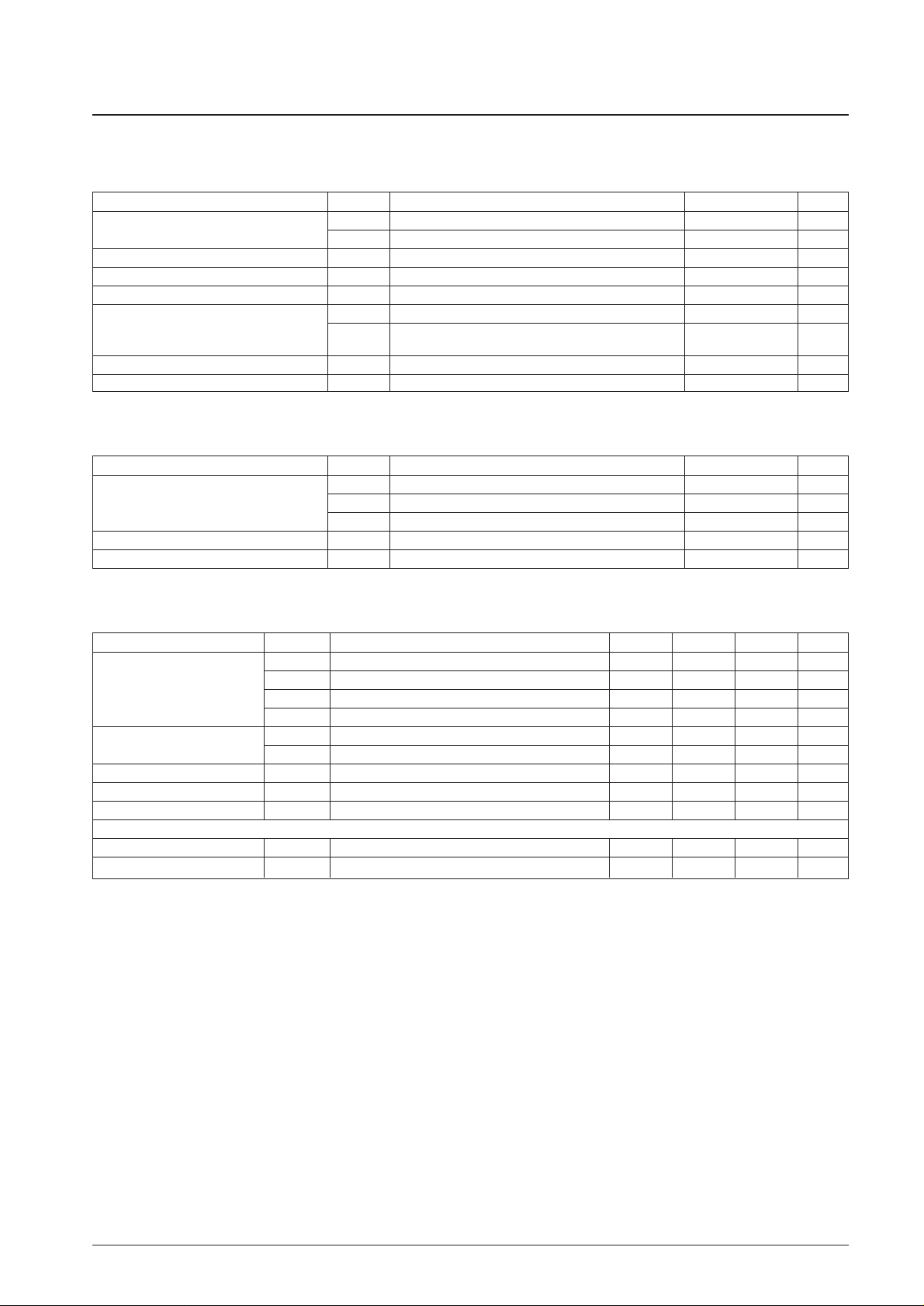
Absolute Maximum Ratings at Ta = 25°C
Allowable Operating Ranges at Ta = 25°C
Electrical Characteristics at Ta = 25°C, VCC= VS= 3 V
No. 4179-2/7
LB1832V
Parameter Symbol Conditions Ratings Unit
Maximum supply voltage
V
CC
max –0.3 to +8.0 V
V
S
max –0.3 to +8.0 V
Output applied voltage V
OUT
–0.3 to VS+ V
SF
V
Input applied voltage V
IN
–0.3 to +0.8 V
GND pin current I
GND
2.0 A
Pd max1 Independent IC 550 mW
Allowable power dissipation
Pd max2
Mounted on the specified printed circuit board
1000 mW
(40
× 30 × 1.5 mm3glass epoxy)
Operating temperature Topr –20 to +75 °C
Storage temperature Tstg –40 to +150 °C
Parameter Symbol Conditions Ratings Unit
V
E
VCC= VS; Using the same power supply 1.6 to 7.0 V
Supply voltage V
CC
Using separate power supplies for VCCand V
S
2.5 to 7.0 V
V
S
1.0 to 7.0 V
Input high-level voltage V
IH
1.6 to 7.0 V
Input low-level voltage V
IL
–0.3 to +0.4 V
Parameter Symbol Conditions min typ max Unit
I
CC
0 Standby: ICC+ I
S
0.1 3 µA
Current drain
I
CC
1 I
CC
3.5 5 mA
I
S
1 Forward/reverse: I
S
65 85 mA
I
S
2 Brake: I
S
60 80 mA
Output saturation voltage
V
O
(sat)1 I
OUT
= 500 mA (VCC= VS= 2 V) 0.3 0.4 V
(upper + lower) V
O
(sat)2 I
OUT
= 1 A (VCC= VS= 2.2 V) 0.6 0.8 V
Variation in output applied voltage I
OUT
= 500 mA –20 0 +20 %
Sustainable output voltage V
O (SUS)IOUT
= 1 A 9 V
Input current I
IN
VIN= 5 V, VCC= 7 V 100 µA
[Spark killer diode]
Reverse current I
S
(leak) VCC, VS= 7 V 10 µA
Forward voltage V
SF
I
OUT
= 1 A 1.7 V
Page 3
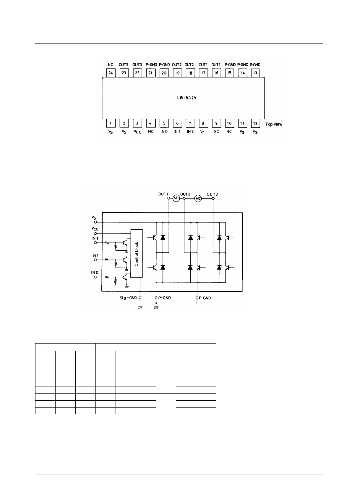
Pin Assignment
Note: 1. VS(motor power supply pins)
Connect either pins 1 and 2 or pins 11 and 12. The wiring resistance falls if all four are connected.
2. P-GND (motor power supply ground pins)
Connect all four of these pins
3. S-GND (Control power supply ground pin)
Connect to the microprocessor ground.
Block Diagram
Note: The two P-GND pins must be connected to a ground as close as possible to the IC.
Truth Table
Note: Blanks are off.
No. 4179-3/7
LB1832V
Input Output
Mode
IN0 IN1 IN2 OUT1 OUT21 OUT3
L L L
Standby
H L L
L H L H L Forward
L L H L H ch1 Reverse
L H H L L Brake
H H L L H Forward
H L H H L ch2 Reverse
H H H L L Brake
Page 4
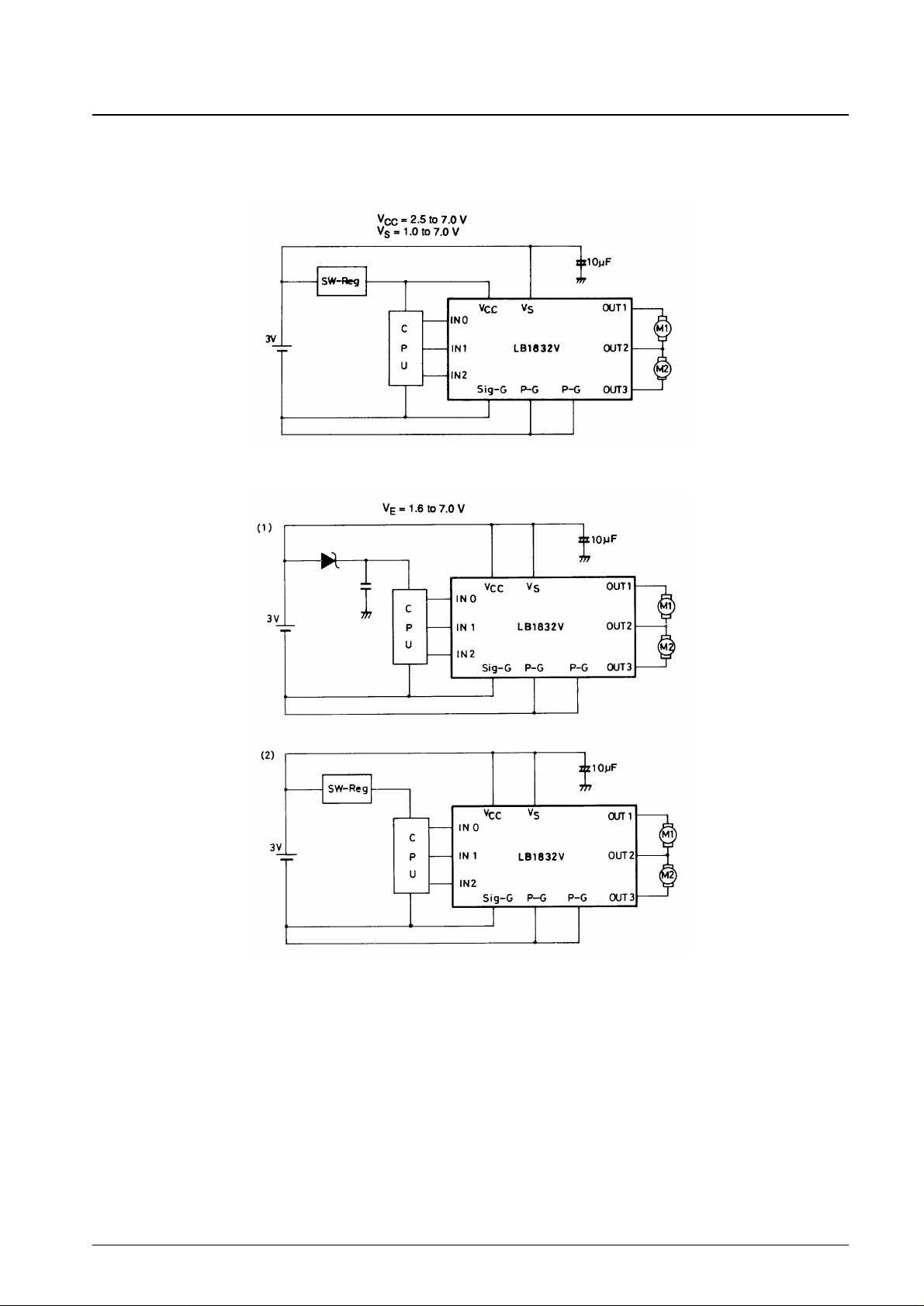
Application Circuit Examples
When separate power supplies are used for VCCand V
S
When the same power supply is used for VCCand V
S
Note: There are no limitations on the magnitude relationships between VCC, VS, and VIN.
No. 4179-4/7
LB1832V
Page 5
No. 4179-5/7
LB1832V
Page 6
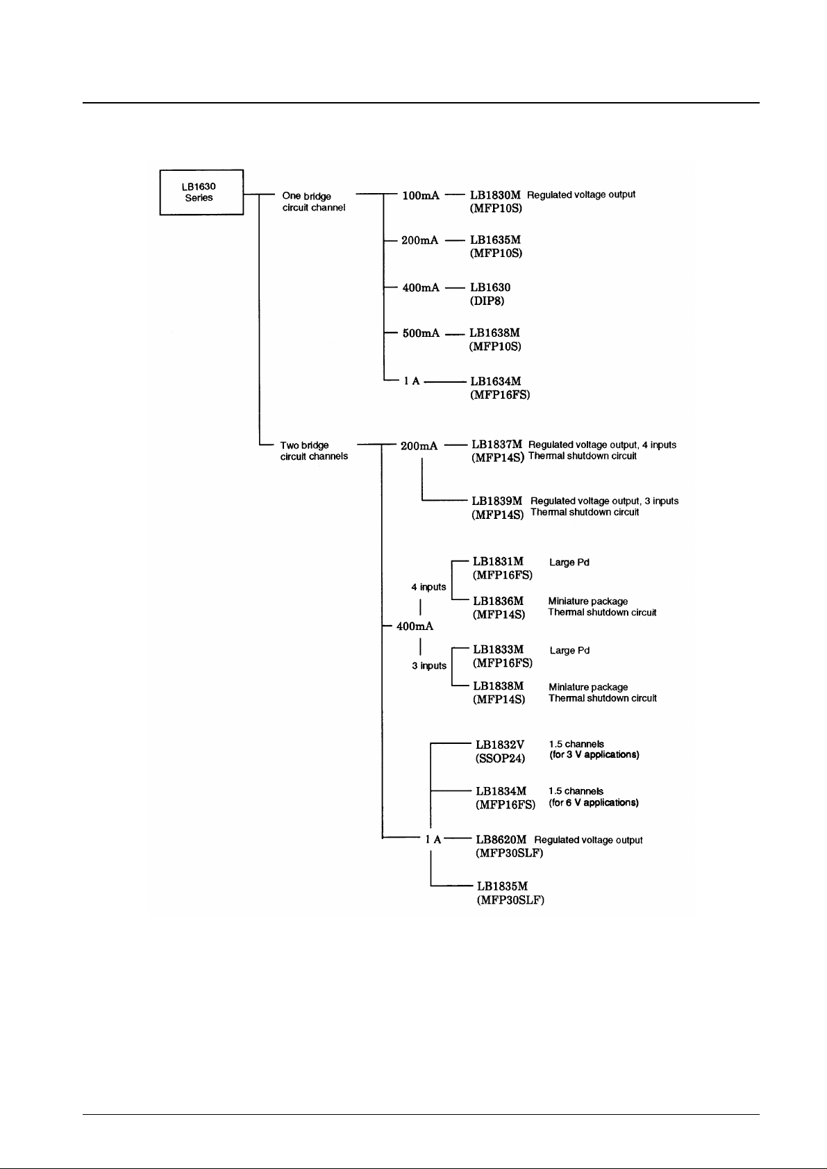
Low-Voltage Low-Saturation Bidirectional Motor Driver Product Line
No. 4179-6/7
LB1832V
Page 7

PS No. 4179-7/7
LB1832V
This catalog provides information as of April, 1996. Specifications and information herein are subject to change
without notice.
■ No products described or contained herein are intended for use in surgical implants, life-support systems, aerospace
equipment, nuclear power control systems, vehicles, disaster/crime-prevention equipment and the like, the failure of
which may directly or indirectly cause injury, death or property loss.
■ Anyone purchasing any products described or contained herein for an above-mentioned use shall:
➀ Accept full responsibility and indemnify and defend SANYO ELECTRIC CO., LTD., its affiliates, subsidiaries and
distributors and all their officers and employees, jointly and severally, against any and all claims and litigation and all
damages, cost and expenses associated with such use:
➁ Not impose any responsibility for any fault or negligence which may be cited in any such claim or litigation on
SANYO ELECTRIC CO., LTD., its affiliates, subsidiaries and distributors or any of their officers and employees
jointly or severally.
■ Information (including circuit diagrams and circuit parameters) herein is for example only; it is not guaranteed for
volume production. SANYO believes information herein is accurate and reliable, but no guarantees are made or implied
regarding its use or any infringements of intellectual property rights or other rights of third parties.
 Loading...