

Page 1
Overview
The LB1695 is a three-phase brushless motor driver IC
that is optimal for DC fan motor drive in home appliances
such as on-demand water heaters.
Features
• Three-phase brushless motor drive
• 45-V voltage handling capacity, 2-A output current
• Current limiter circuit
• Low-voltage protection circuit
• Thermal shutdown protection circuit
• Hall amplifiers with hysteresis characteristics
• FG output function
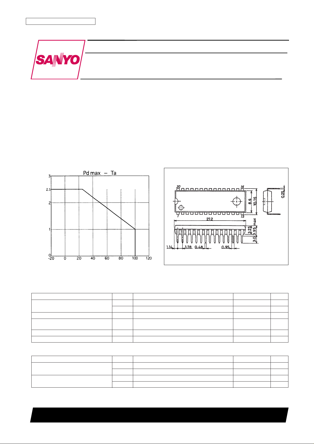
Package Dimensions
unit: mm
3196-DIP30SD
Monolithic Digital IC
Ordering number : EN5678
63097HA(OT) No. 5678-1/7
SANYO: DIP30SD
[LB1695]
SANYO Electric Co.,Ltd. Semiconductor Bussiness Headquarters
TOKYO OFFICE Tokyo Bldg., 1-10, 1 Chome, Ueno, Taito-ku, TOKYO, 110 JAPAN
Three-Phase Brushless Motor Driver
LB1695
Parameter Symbol Conditions Ratings Unit
Supply voltage
V
CC
10 V
V
M
45 V
Output current I
O
2.0 A
Allowable power dissipation Pd max
Mounted on a printed circuit board (114.3
× 76.2 × 1.6 mm
3
2.5 W
glass-epoxy board)
Operating temperature Topr –20 to +100 °C
Storage temperature Tstg –55 to +150 °C
Specifications
Absolute Maximum Ratings at Ta = 25°C
Parameter Symbol Conditions Ratings Unit
Power-supply voltage range
V
CC
4.5 to 5.5 V
V
M
5 to 42 V
Maximum power-supply slew rate at power on
∆V
CC
/∆t At VCC= V
LVSD
(OFF)* No more than 0.04 V/µs
∆V
M
/∆t At VM= 0 V* No more than 0.16 V/µs
Note: *These items are stipulated because output through currents can occur if the speed with which the power-supply voltage rises is too fast when power is
first applied.
Allowable Operating Ranges at Ta = 25°C
With a 20% wiring density on
a glass-epoxy board
114.3 × 76.2 × 1.6 mm
3
Ambient temperature, Ta – °C
Allowable power dissipation, Pdmax – W
Page 2
No. 5678-2/7
LB1695
Parameter Symbol Conditions
Ratings
Unit
min typ max
Current drain I
CC
Forward rotation 13 19 mA
Output saturation voltage V
O
(sat)1 IO= 0.5 A, VO(sink) + VO(source) 1.8 2.4 V
V
O
(sat)2 IO= 1.0 A, VO(sink) + VO(source) 2.1 2.8 V
Output leakage current I
O
leak 100 µA
[Hall Amplifier]
Input bias current I
HB
1 4 µA
Common-mode input voltage range V
ICM
1.5 3.2 V
Hysteresis ∆V
IN
21 30 37 mV
Input voltage (low → high) V
SLH
5 15 25 mV
Input voltage (high → low) V
SHL
–25 –15 –5 mV
[FG Pin] (Speed pulse output)
Output low-level voltage V
FGLIFG
= 5 mA 0.4 V
Pull-up resistance R
FG
7.5 10.0 12.5 kΩ
[Forward/Reverse Operation]
Forward V
FR1
0 0.8 V
Reverse V
FR2
4.2 5.0 V
[Current Limiter Operation]
Limiter V
RF
0.42 0.5 0.6 V
[Thermal Shutdown Operation]
Operating temperature TSD * 150 180 °C
Hysteresis ∆TSD * 40 °C
[Low-Voltage Protection Operation]
Operating voltage V
LVSD
3.5 3.8 4.1 V
Release voltage V
LVSD(OFF)
4.3 4.5 V
Hysteresis ∆V
LVSD
0.4 0.5 0.6 V
[Pin C]
Charge current I
CL
R = 33 kΩ 30 40 50 µA
Discharge current I
CH
R = 33 kΩ 90 120 150 µA
Charge start voltage V
CL
R = 33 kΩ 0.3 0.4 0.5 V
Discharge start voltage V
CH
R = 33 kΩ 1.5 2.0 2.5 V
Output current ignored time t
sm
R = 33 kΩ, C = 4700 pF 58 68 78 µs
Output off time t
so
R = 33 kΩ, C = 4700 pF 164 193 222 µs
Electrical Characteristics at Ta = 25°C, VCC= 5 V, VM= 30 V
Note: *The items marked with an asterisk are design target values and are not tested.
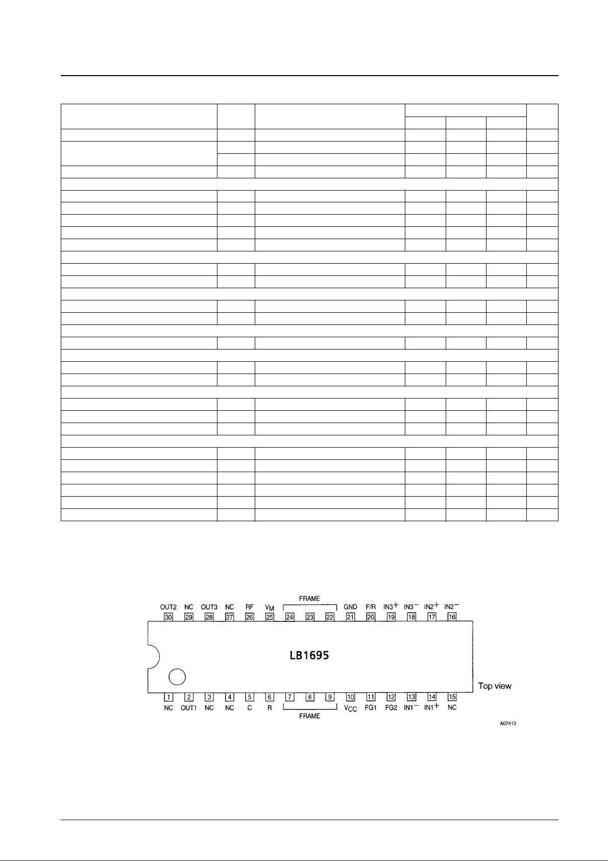
Pin Assignment
Page 3
No. 5678-3/7
LB1695
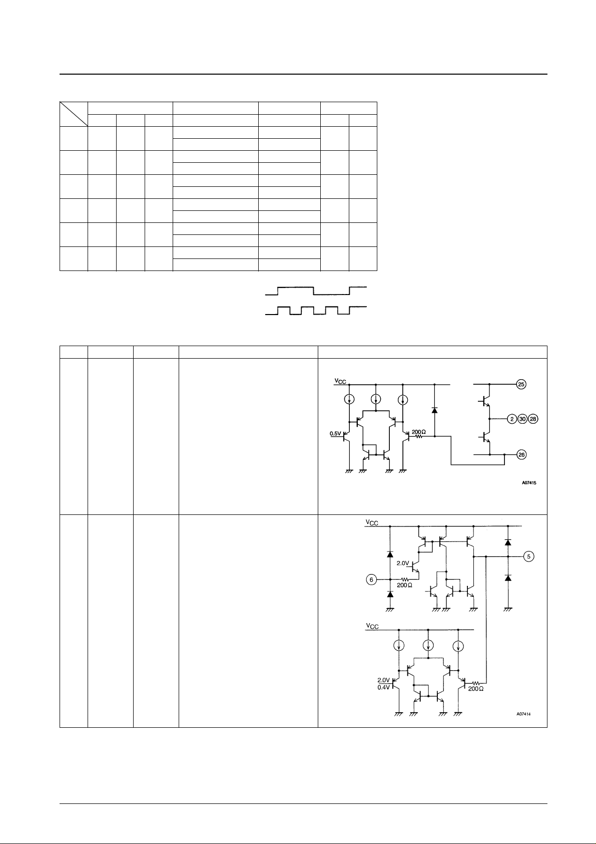
Truth Table
F/R
Forward (low): 0.0 to 0.8 V
Reverse (high): 4.2 to 5.0 V
FG Output
Input Forward/reverse control Output FG output
IN1 IN2 IN3 F/R Source → sink FG1 FG2
1 H L H
L OUT2 → OUT1
L L
H OUT1 →OUT2
2 H L L
L OUT3 → OUT1
L H
H OUT1 →OUT3
3 H H L
L OUT3 → OUT2
L L
H OUT2 →OUT3
4 L H L
L OUT1 → OUT2
H H
H OUT2 →OUT1
5 L H H
L OUT1 → OUT3
H L
H OUT3 →OUT1
6 L L H
L OUT2 → OUT3
H H
H OUT3 →OUT2
Pin Functions
Pin No. Pin Pin voltage(V) Pin function Equivalent circuit
2
30
28
25
26
OUT1
OUT2
OUT3
V
M
RF
• Output pin 1
• Output pin 2
• Output pin 3
• Power supply pin that provides the
output
• Output current detection
Connect the resistor Rf between this pin
and ground.
• The current limiter limits the output
current to the value set by V
RF
/Rf
(current limiter operation).
5
6
C
R
• The capacitor connected to this pin
determines both the time the output is
turned off when the current limiter
operates and the time the output current
is ignored.
• The resistor connected to this pin
determines the charge current for the pin
C capacitor.
Continued on next page.
FG1
FG2
Page 4
No. 5678-4/7
LB1695
Continued from preceding page.
Pin No. Pin Pin voltage(V) Pin function Equivalent circuit
7, 8,
9, 22,
23, 24
FRAME
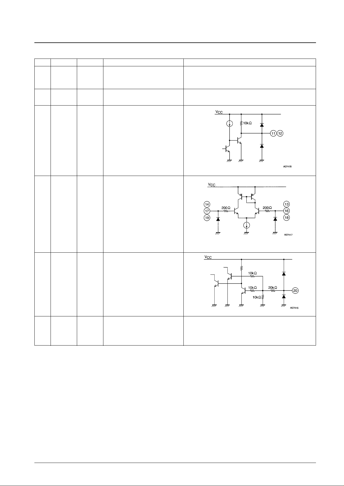
• This pin is used for heat dissipation.
Electrically, it must be left open.
10 V
CC
• Power for all circuits other than the
output block.
11
12
FG1
FG2
• First speed pulse output. A pull-up
resistor is built in.
• Second speed pulse output. A pull-up
resistor is built in.
13
14
16
17
18
19
IN1
–
IN1
+
IN2
–
IN2
+
IN3
–
IN3
+
1.5 V min
V
CC
–1.8V
max
• Hall element input
Logic high is defined as IN
+
> IN–.
• Hall element input
Logic high is defined as IN
+
> IN–.
• Hall element input
Logic high is defined as IN
+
> IN–.
20 F/R 0.0 V min
V
CC
max
• Forward/reverse control
21 GND
• Ground for all circuits other than the
output block.
The lowest potential of the output
transistors will be the potential of the Rf
pin.
Page 5
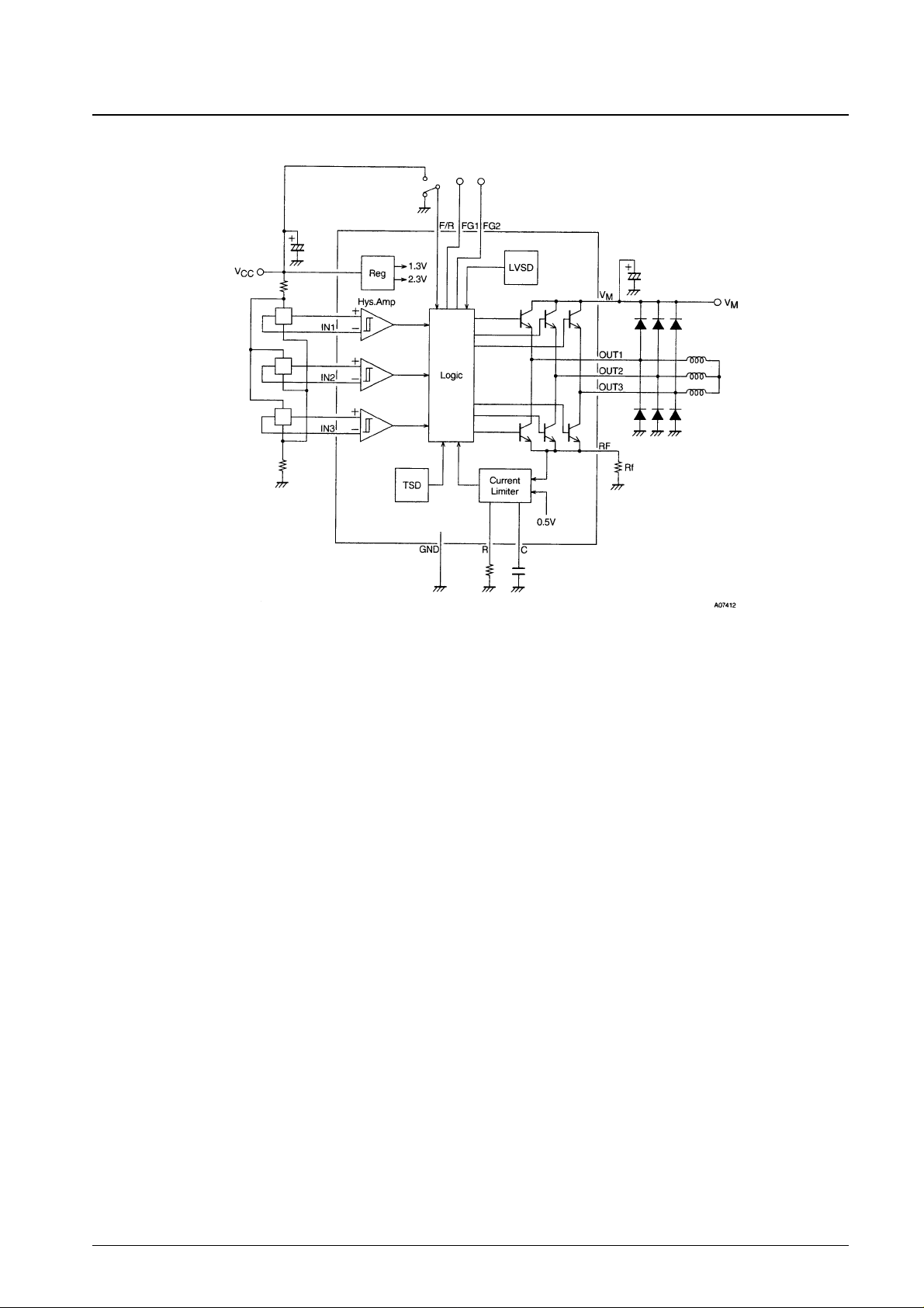
Block Diagram and Peripheral Circuits
LB1695 Functional Description
1.Hall element input circuits
The Hall element input circuits are differential amplifiers with a hysteresis of about 30 mV (typical). The operating DC
level must be within the common-mode input voltage range (1.5 V to VCC– 1.8 V). We recommend providing input
levels that exceed the hysteresis by at least a factor of three (120 to 160 mVp-p) to assure that circuit operation is not
affected by noise. If the ability to withstand noise is determined to be a problem during noise evaluation or other
testing, insert capacitors (of about 0.01 µF) between the Hall input IN+and IN–pins.
2.Protection circuit
2.1 Low-voltage protection circuit
The sink side output transistors are turned off if the VCCvoltage falls below the stipulated voltage (V
LVSD
). This
circuit prevents incorrect operation when the VCCvoltage is reduced.
2.2 Thermal shutdown circuit
The sink side output transistors are turned off if the junction temperature exceeds the stipulated temperature (TSD).
This circuit prevents the IC from being destroyed by overheating. Applications must be designed so that this circuit
does not operate except in unusual situations.
3.FG output circuit
The LB1695 combines the IN1, IN2, and IN3 inputs and then wave shapes the combined signal. The FG1 output has
the same frequency as the Hall inputs, and the FG2 output has a frequency three times that of the Hall inputs.
4.Forward/reverse control circuit
This circuit was designed with the assumption that the direction will not be switched from the F/R pin while the motor
is turning. If the direction is switched while the motor is turning, through currents will flow in the output and ASO will
become a problem. We recommend only using F/R switching when the VMpower supply is in the off state, i.e. with the
motor in the stopped state.
5.VCCand VMpower supplies
If the speed with which the power-supply voltages (VCCand VM) rise when power is first applied is too fast, through
currents will flow in the output and ASO will become a problem. Applications must assure that the power supply rise
speeds do not exceed 0.04 V/µ s (∆VCC/∆t) and 0.16 V/µ s (∆VM/∆t). When applying power, it is desirable to apply
VCCfirst and then apply VM. When turning the power off, it is desirable to first turn off VM, then to wait for the motor
to stop, and only then turn off VCC. If VCCis turned off after VMis turned off but while the motor is still turning due to
No. 5678-5/7
LB1695
Page 6

inertia, certain motor types may cause the VMvoltage at the IC to rise and generate voltages that exceed the voltage
handling capacity of the IC.
6.Power supply stabilization capacitor
The low-voltage protection circuit may operate or other problems may occur if large fluctuations occur in the VCCline
voltage. The VCCline must be stabilized by a capacitor (of a few µ F) inserted between VCCand ground. Also, the large
switching currents that flow in the VMline can cause fluctuations in the IC VMvoltage due to inductive components in
the circuit wiring. The VMline must also be stabilized by a capacitor inserted between VMand ground to prevent
fluctuations in the ground line potential, incorrect operation, and voltages that exceed the voltage handling capacity of
the IC. In particular, applications that have long circuit lines for VM, VCC, and ground must have adequate stabilization
capacitors inserted in the power lines.
7.Current limiter circuit
The current limiter circuit turns off the sink side output transistors when the output current reaches the set limit value
(the limit current). The RF pin is used for current detection, and the output current is detected as a voltage by inserting
the resistor Rfbetween the RF pin and ground. The current limiter circuit operates when the RF pin reaches 0.5 V
(typical), and thus the output current is limited to the current limit set by the term 0.5/Rf.
7.1 Output off time
After the current limiter circuit operates and turns off the sink side output transistors, it then turns the output on again
after a fixed period (the output off time) has elapsed. This current limiter circuit output switching technique adopted in
the LB1695 is much less susceptible to problems with ASO than are output limitation techniques in which the output is
not operated at the saturated level. The output off time it determined by the charge time for the capacitor connected to
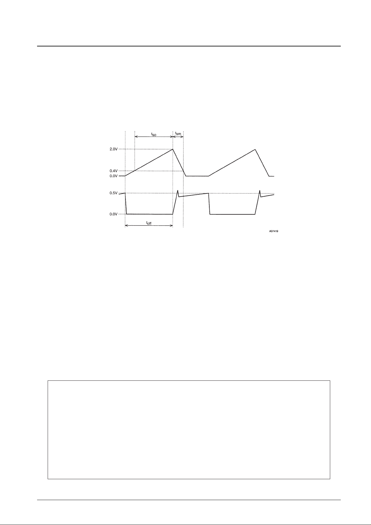
the C pin. When the current limiter circuit operates, the C pin capacitor begins to charge, and the time required to charge
this capacitor to the C voltage, which is 2 volts (typical), is the output off time. When the capacitor is charged to the C
voltage of 2 volts, the sink side output transistors are turned on again. The C pin charge current is a fixed current
determined by the resistor R connected to the R pin. The capacitor charge current ICLand the output off time t
off
are
related as follows.
ICL≈ 1.3/R (R must be set to a value in the range 13 to 100 kΩ)
t
off
≈ C/ICL× 2.0
≈ 1.53 × R × C
7.2 Output current ignored time
While the current limiter circuit is operating and the sink side output is off, a regenerative current flows in the
external diode provided to absorb regenerative currents in the upper side of the output circuit that was turned off.
When the sink side output is turned off after the output off time has elapsed, a reverse current flows instantaneously
in this diode due to the diode’s reverse recovery time. Due to this phenomenon, a current that may reach the current
limit value flows instantaneously in the output. If the current limiter operated again due to this current, the output
would be turned off and the average current level would fall. This could result in significantly lower torque during,
for example, motor startup. Therefore, to prevent this current from being detected, the current limiter circuit also
provides a fixed period (the output current ignored time) during which the output current is not detected at the point
where the sink side output is turned on again after being turned off. The output current ignored time is determined
by the discharge time for the capacitor connected to the C pin. This discharge starts at the point where the capacitor
is charged to 2 volts following operation of the current limiter circuit. The output current ignored time is the time
for the capacitor to discharge to 0.4 volts (typical). The capacitor discharge current is a fixed current and is set to be
a current about three times the charge current. Therefore, the output current ignored time is about 1/3 the output off
time. The capacitor discharge current ICHand the output current ignored time tsmare related as follows.
ICH≈ 1.3/R × 3
tsm≈ C/ICH× 1.6
≈ 0.41 × R × C
Since the current limiter circuit provides a slope to the on time when the sink side output is turned on again, the
reverse circuit never becomes significantly large, even if a rectifying diode (i.e. a diode whose reverse recovery
time is not particularly short) is used as the regenerative current absorption external diode.
7.3 Output off time setting
The output off time must be set to a period optimal for the type of motor used. This time is set by the values of the
external resistor attached to the R pin and the external capacitor attached to the C pin. Figure 1 shows the
waveforms during current limiter operation.
No. 5678-6/7
LB1695
Page 7
No. 5678-7/7
LB1695
This catalog provides information as of June, 1997. Specifications and information herein are subject to change
without notice.
■ No products described or contained herein are intended for use in surgical implants, life-support systems, aerospace
equipment, nuclear power control systems, vehicles, disaster/crime-prevention equipment and the like, the failure of
which may directly or indirectly cause injury, death or property loss.
■ Anyone purchasing any products described or contained herein for an above-mentioned use shall:
➀ Accept full responsibility and indemnify and defend SANYO ELECTRIC CO., LTD., its affiliates, subsidiaries and
distributors and all their officers and employees, jointly and severally, against any and all claims and litigation and all
damages, cost and expenses associated with such use:
➁ Not impose any responsibility for any fault or negligence which may be cited in any such claim or litigation on
SANYO ELECTRIC CO., LTD., its affiliates, subsidiaries and distributors or any of their officers and employees
jointly or severally.
■ Information (including circuit diagrams and circuit parameters) herein is for example only; it is not guaranteed for
volume production. SANYO believes information herein is accurate and reliable, but no guarantees are made or implied
regarding its use or any infringements of intellectual property rights or other rights of third parties.
(1) If a shorter output off time is used:
Since the output off time and the output current ignored time are set to have a ratio of about 3:1 by IC internal circuits, it
is not possible to set these periods independently. Thus the output current ignored period may become insufficient if the
output off time is set to an excessively short period. If the output current ignored period is too short, the reverse current
in the regenerative current absorption external diode may cause the current limiter circuit to operate. (See Section 7.2.)
Also, if the output off time is decreased, the diode reverse current will increase and ASO may become a problem.
(2) If a longer output off time is used:
If an excessively long output off time is used, the average current will decrease resulting in reduced torque during
motor startup. For some motor types, this may make it impossible to switch from the current limiter operating state
to steady state operation.
Figure 1. Current Limiter Operating Waveforms
8.IC internal power dissipation calculation
Pd = (VCC× ICC) + (VM× IM) – (power dissipated in the motor coils)
9.Techniques for measuring IC internal temperature increases
Since it is not possible to measure the IC internal temperature directly, one of the following techniques is normally
used for temperature measurement.
9.1 Thermocouple measurement
When using a thermocouple for temperature measurement, the thermocouple is attached to a fin on the heat sink.
While this measurement technique is simple, it suffers from large measurement errors when the thermal generation
process is not at steady state.
9.2 Measurement using IC internal diode properties
We recommend using the properties of the parasitic diode that exists between FG1 and ground for measuring the
temperature of this IC. Set FG1 to the high (off) state and measure the VFvoltage of the parasitic diode. Then
calculate the temperature from the temperature characteristics of the VFvoltage.
C pin voltage
RF pin voltage
 Loading...