

Page 1

Overview
The LB1845 is a PWM current control type stepping
motor driver that uses a bipolar drive scheme. It is
particularly suitable for driving carriage and paper feed
stepping motors in printers and similar products.
Features
• PWM current control (fixed off time scheme)
• Digital load current selection function
• Sustained output voltage: 45 V
• Built-in thermal shutdown circuit
Package Dimensions
unit: mm
3147A-DIP28H
Monolithic Digital IC
Ordering number: EN5505B
D3096HA (OT) No. 5505-1/7
SANYO: DIP28H
[LB1845]
SANYO Electric Co.,Ltd. Semiconductor Bussiness Headquarters
TOKYO OFFICE Tokyo Bldg., 1-10, 1 Chome, Ueno, Taito-ku, TOKYO, 110 JAPAN
PWM Current Control Stepping Motor Driver
LB1845
Parameter Symbol Conditions Ratings Unit
Motor supply voltage V
BB
45 V
Peak output current I
OPEAKtW
= 20 µS 1.75 A
Continuous output current I
OMAX
1.5 A
Logic block supply voltage V
CC
7.0 V
Logic input voltage range V
IN
–0.3 to V
CC
V
Emitter output voltage V
E
1.0 V
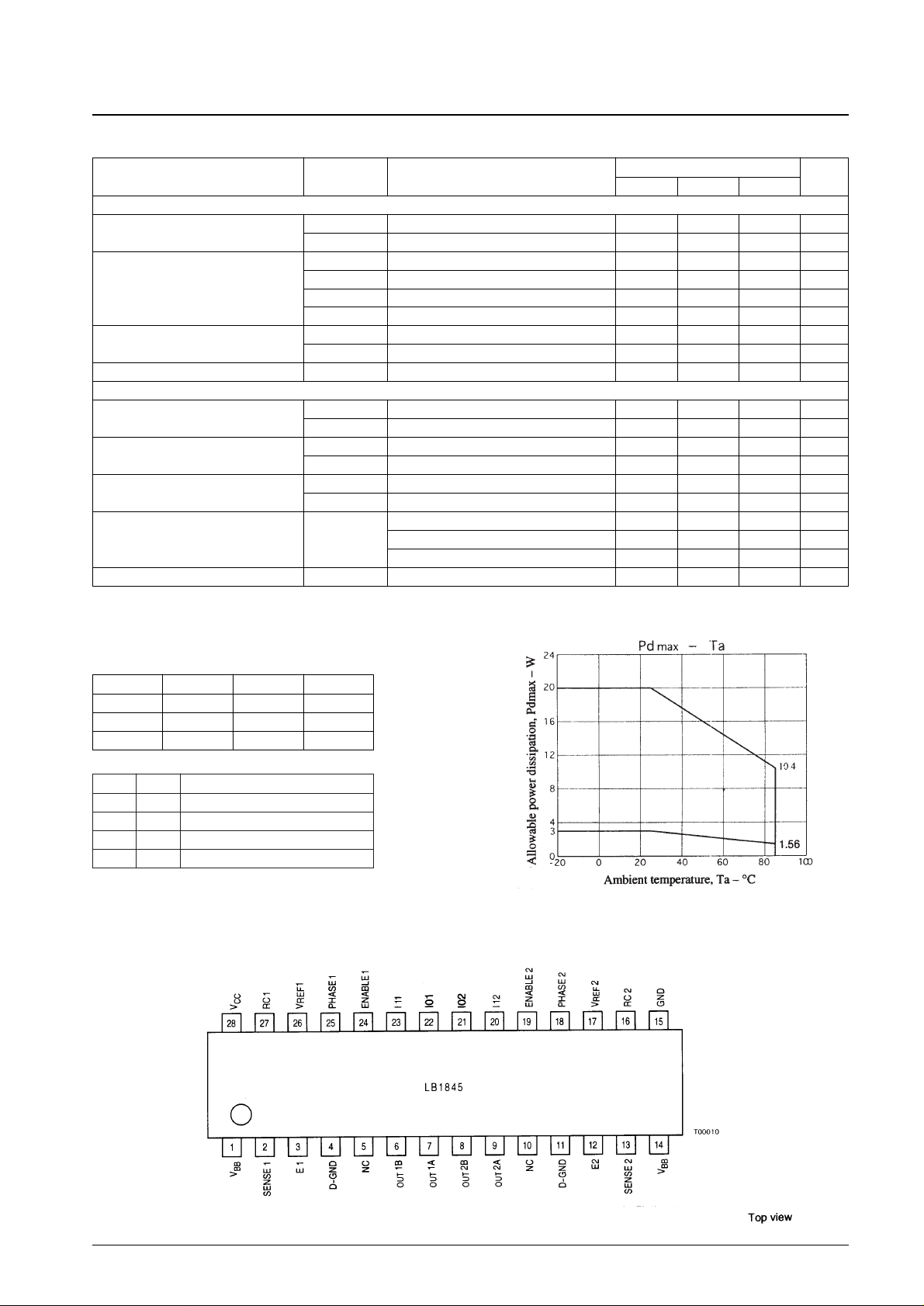
Allowable power dissipation
Pd max1 Independent IC 3.0 W
Pd max2 With an arbitrarily large heat sink 20.0 W
Operating temperature Topr –20 to +85 °C
Storage temperature Tstg –55 to +150 °C
Specifications
Absolute Maximum Ratings at Ta = 25°C
Parameter Symbol Conditions Ratings Unit
Motor supply voltage V
BB
10 to 44.5 V
Logic block supply voltage V
CC
4.75 to 5.25 V
Reference voltage V
REF
1.5 to 7.5 V
Recommended Operating Ranges at Ta = 25°C
Page 2
No. 5505-2/7
LB1845
Parameter Symbol Conditions
Ratings
Unit
min typ max
[Output Block]
Output stage supply voltage
I
BB ON
12 16 mA
I
BB OFF
0.7 0.9 mA
V
O
(sat)1 IO= +1.0 A sink 1.2 1.4 V
Output saturation voltage 1
V
O
(sat)2 IO= +1.5 A sink 1.4 1.7 V
V
O
(sat)3 IO= –1.0 A source 1.1 1.3 V
V
O
(sat)4 IO= –1.5 A source 1.3 1.6 V
Output leakage current
I
O
(leak)1 VO= VBBsink 50 µA
I
O
(leak)2 VO= 0 V source –50 µA
Sustained output voltage V(sus) * 45 V
[Logic Block]
Logic supply current
I
CC ON
I0 = 0.8 V, I1 = 0.8 V 19.5 25.3 mA
I
CC OFF
I0 = 2.4 V, I1 = 2.4 V 15.5 20.1 mA
Input voltage
V
IH
2.4 V
V
IL
0.8 V
Input current
I
IH
VIH= 2.4 V 10 µA
I
IL
VIL= 0.8 V –10 µA
I0 = 0.8 V, I1 = 0.8 V 9.5 10 10.5
Current control threshold voltage V
REF/VSENSE
I0 = 2.4 V, I1 = 0.8 V 13.5 15 16.5
I0 = 0.8 V, I1 = 2.4 V 25.5 30 34.5
Thermal shutdown temperature T
S
170 °C
Electrical Characteristics at Ta = 25°C, VBB= 38 V, VCC= 5 V, V
REF
= 5 V
Truth Table
Pin Assignment
Note: *Design guaranteed value
Note: Outputs go off when ENABLE is high or in the I0 = I1 = high state.
ENABLE PHASE OUT A OUT B
L H H L
L L L H
H — OFF OFF
I0 I1 Output current
L L V
REF
/ (10 × RE) = I
OUT
H L V
REF
/ (15 × RE) = I
OUT
× 2/3
L H V
REF
/ (30 × RE) = I
OUT
× 1/3
H H 0
Page 3

Block Diagram
Application Circuit Diagram
No. 5505-3/7
LB1845
Page 4
Pin Functions
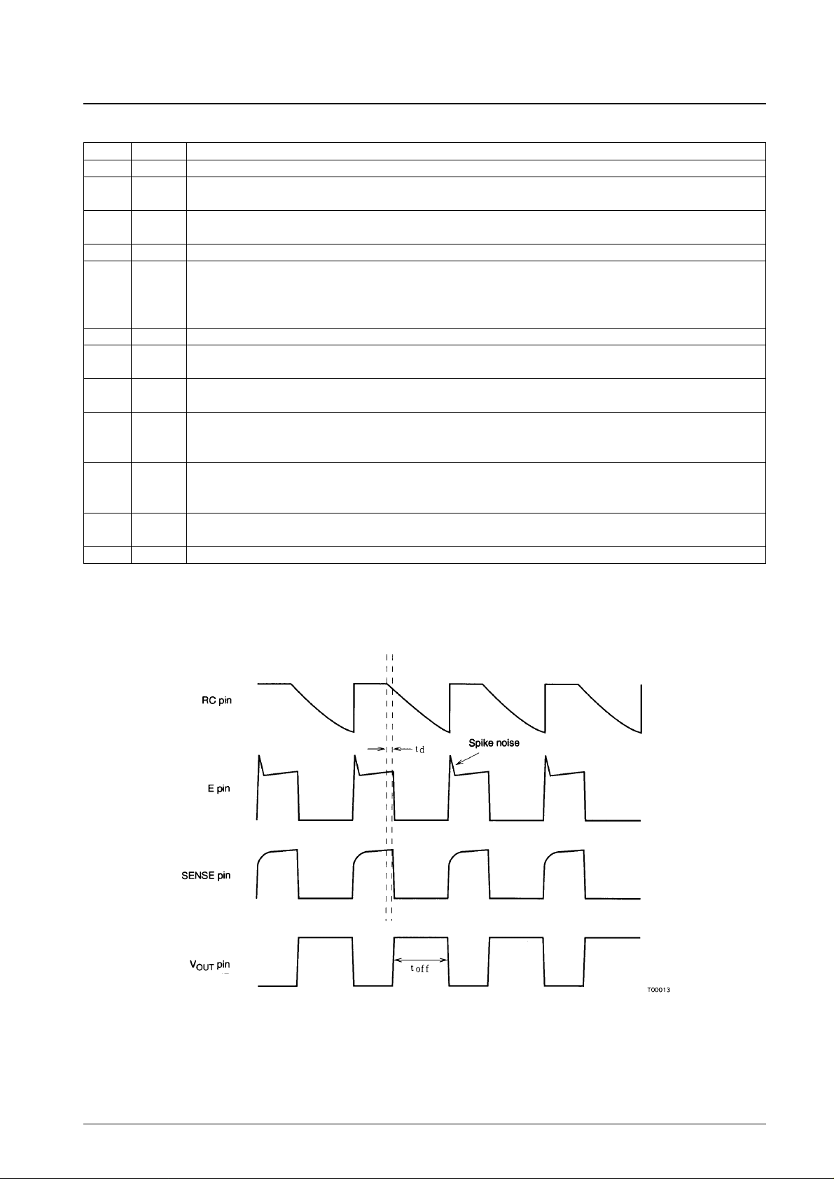
Timing chart for pin switching operations during PWM drive
Figure 1 Switching Waveforms
toff: Output off time. Determined by external capacitor and resistor Ct and Rt. (toff = Ct × Rt)
td: Delay time between the point the set current is sensed at the SENSE pin and the point the output turns off.
No. 5505-4/7
LB1845
Pin no. Pin Function
1, 14 V
BB
Output stage power-supply voltage
2 SENSE1 Set current detection pins.
13 SENSE2 Connect these pins, fed back through noise filters, to E1 and E2.
3 E1 The set current is controlled by the resistors Re inserted between these pins and ground.
12 E2
4, 11 D-GND Internal diode anode connection
6 OUT 1B Outputs
7 OUT 1A
8 OUT 2B
9 OUT 2A
15 GND Ground
27 RC1 Used to set the output off time for the switched output signal.
16 RC2 The fixed off times are set by the capacitors and resistors connected to these pins. toff = CR.
26 V
REF
1 Output current settings
17 V
REF
2 The output current is determined by the voltage (in the range 1.5 to 7.5 V) input to these pins.
25 PHASE1 Output phase switching inputs.
18 PHASE2 High-level input: OUT A = high, OUT B = low
Low-level input: OUT A = low, OUT B = high
24 ENABLE1 Output on/off settings
19 ENABLE2 High-level input: output off
Low-level input: output on
22, 23 I01, I11 Digital inputs that set the output current
21, 20 I02, I12 The output currents can be set to 1/3, 2/3, or full by setting these pins to appropriate combinations of high and low levels.
28 V
CC
Logic block power supply
Page 5
Usage Notes
1.External diode
Since this IC adopts a system based on lower side transistor switching drive, an external diode for the regenerative
current that occurs during switching is required between VBBand V
OUT
. Use a Schottky barrier diode with a low
feedthrough current.
2.Noise filters
Since spike noise (see Figure 1) occurs when switching to the on state due to the external diode’s feedthrough current,
applications must remove noise from the SENSE pin with a noise filter (Cc, Rc) between the E pin and the SENSE pin.
However, note that if the values of Cc and Rc are too large, the SENSE voltage rise will be slowed, and the current
setting will be shifted towards a higher current level.
3.V
REF
pin
It is possible to change the output current continuously by continuously changing the V
REF
pin voltage. However, this
voltage cannot be set to 0 V. The V
REF
pin input impedance is 26 kΩ (±30%) when V
REF
is 5 V. Since this pin is used
to set the output current, applications must be designed so that noise does not appear on this pin's input.
4.GND pin
Since this IC switches large currents, care must be taken to avoid ground loops when the IC is mounted in the
application. The section of the PCB that handles large currents should be designed with a low-impedance pattern, and
must be separated from the small signal sections of the circuit. In particular, the ground for the sense resistor Re must
be as close as possible to the IC ground.
5.Operation in hold mode
There are cases where a current somewhat larger than the current setting may flow in hold mode (light load mode).
Since this IC adopts a lower side switching, lower side sense system, the emitter voltage falls and the sense voltage
goes to 0 when the switching state goes to off. The circuit then always turns the output on after the toff period has
elapsed. At this time, due to the light load, the existence of the time td, and the fact that the output goes on even if the
output current is higher than the set current, the output current will be somewhat higher than the set current.
Applications should set the current setting somewhat lower than required if this occurs.
6.Function for preventing the upper and lower outputs being on at the same time
This IC incorporates a built-in circuit that prevents the through currents that occur when the phase is switched. The
table lists the output on and off delay times when PHASE and EANBLE are switched.
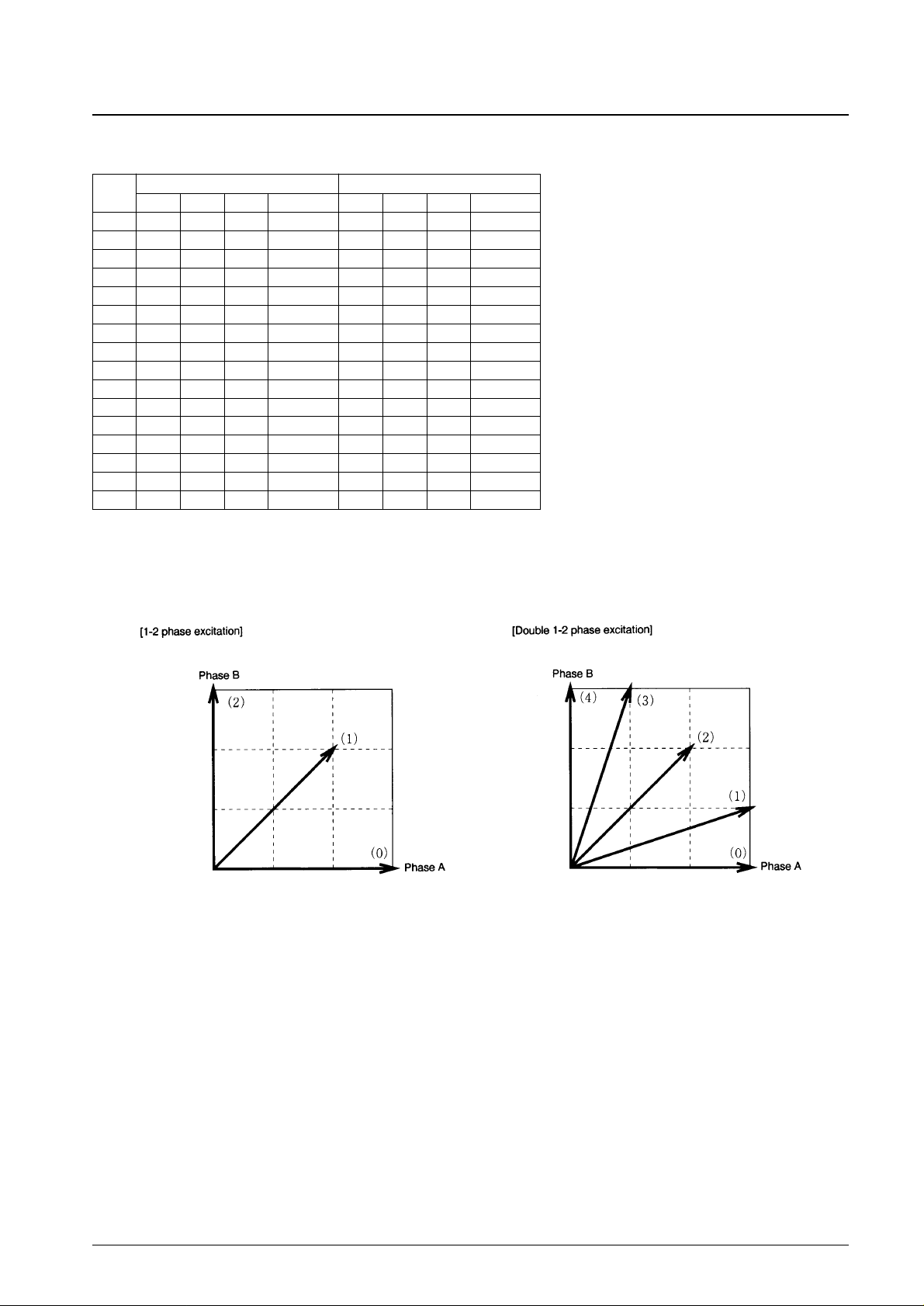
7.1-2 phase excitation and the double 1-2 phase excitation control sequence
To reduce the vibration that occurs when the motor turns, this IC supports 1-2 phase excitation and double 1-2 phase
excitation by using the output current setting digital input pins I0 and I1 without changing the V
REF
pin voltage. Tables
1 and 2 list that control sequence, and Figure 2 and Figure 3 present the composite vector diagram for this sequence.2.
Noise filters
No. 5505-5/7
LB1845
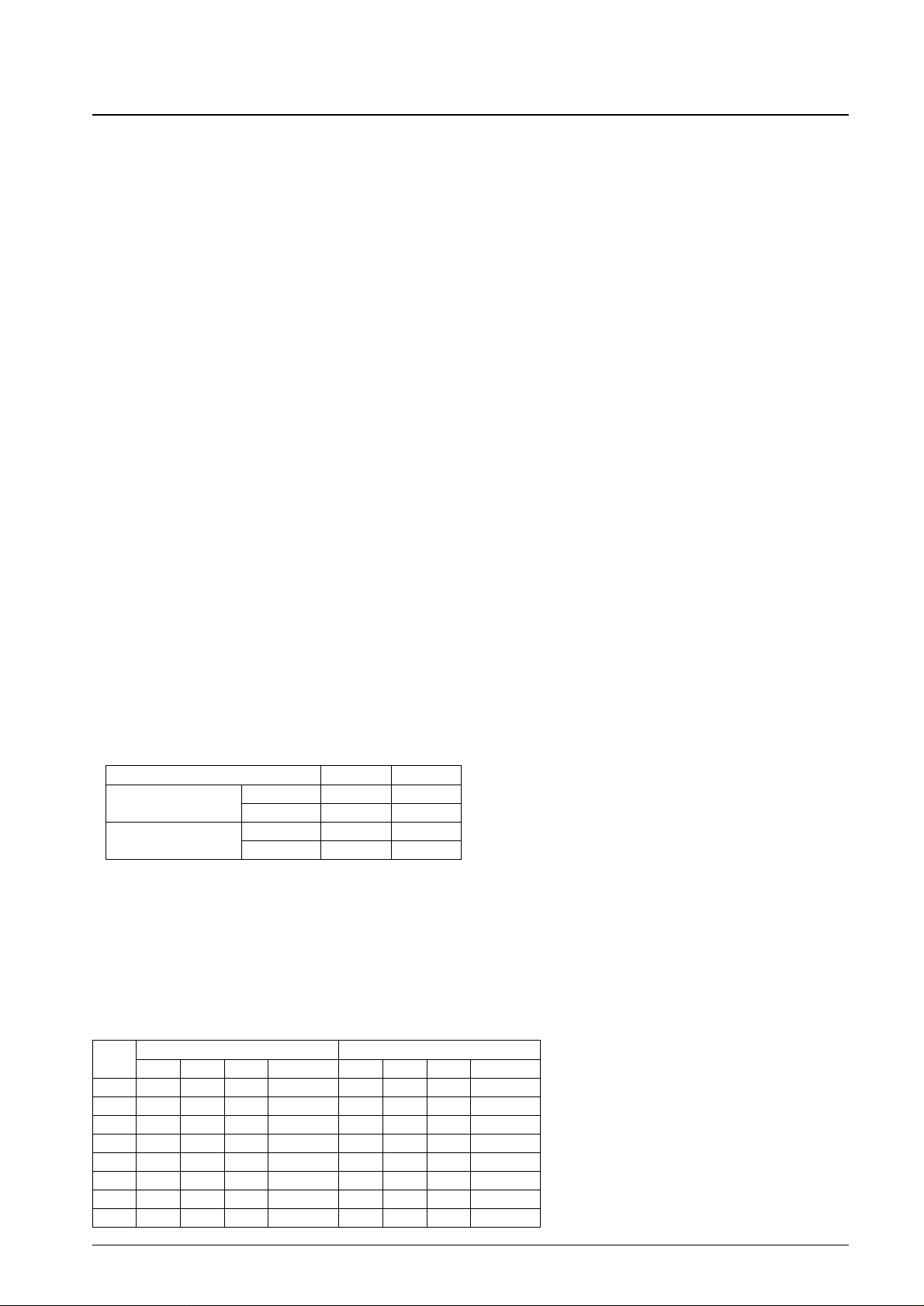
Sink side Source side
When PHASE is switched
On delay time 10 µs 9 µs
Off delay time 1.5 µs 3 µs
When ENABLE is on
On delay time 9 µs 9 µs
Off delay time 1.5 µs 6.5 µs
No.
Phase A Phase B
PH1 I11 I01 Current value PH2 I12 I02 Current value
0 0 0 0 1 * 1 1 0
1 0 0 1 2/3 0 0 1 2/3
2 * 1 1 0 0 0 0 1
3 1 0 1 2/3 0 0 1 2/3
4 1 0 0 1 * 1 1 0
5 1 0 1 2/3 1 0 1 2/3
6 * 1 1 0 1 0 0 1
7 0 0 1 2/3 1 0 1 2/3
Table 1 [1-2 phase excitation] 1/2 step
ENABLE1 = ENABLE2 = 0
Page 6
No. 5505-6/7
LB1845
No.
Phase A Phase B
PH1 I11 I01 Current value PH2 I12 I02 Current value
0 0 0 0 1 * 1 1 0
1 0 0 0 1 0 1 0 1/3
2 0 0 1 2/3 0 0 1 2/3
3 0 1 0 1/3 0 0 0 1
4 * 1 1 0 0 0 0 1
5 1 1 0 1/3 0 0 0 1
6 1 0 1 2/3 0 0 1 2/3
7 1 0 0 1 0 1 0 1/3
8 1 0 0 1 * 1 1 0
9 1 0 0 1 1 1 0 1/3
10 1 0 1 2/3 1 0 1 2/3
11 1 1 0 1/3 1 0 0 1
12 * 1 1 0 1 0 0 1
13 0 1 0 1/3 1 0 0 1
14 0 0 1 2/3 1 0 1 2/3
15 0 0 0 1 1 1 0 1/3
Table 2 [Double 1-2 phase excitation] about 1/4 step
Composite Vector Diagram
Figure 2 Composite Vector Diagram for the
Sequence in Table 1 (1/4 cycle)
Figure 3 Composite Vector Diagram for the
Sequence in Table 2 (1/4 cycle)
ENABLE1 = ENABLE2 = 0
Page 7
No. 5505-7/7
LB1845
This catalog provides information as of December, 1996. Specifications and information herein are subject to
change without notice.
■ No products described or contained herein are intended for use in surgical implants, life-support systems, aerospace
equipment, nuclear power control systems, vehicles, disaster/crime-prevention equipment and the like, the failure of
which may directly or indirectly cause injury, death or property loss.
■ Anyone purchasing any products described or contained herein for an above-mentioned use shall:
➀
Accept full responsibility and indemnify and defend SANYO ELECTRIC CO., LTD., its affiliates, subsidiaries and
distributors and all their officers and employees, jointly and severally, against any and all claims and litigation and all
damages, cost and expenses associated with such use:
➁
Not impose any responsibility for any fault or negligence which may be cited in any such claim or litigation on
SANYO ELECTRIC CO., LTD., its affiliates, subsidiaries and distributors or any of their officers and employees
jointly or severally.
■ Information (including circuit diagrams and circuit parameters) herein is for example only; it is not guaranteed for
volume production. SANYO believes information herein is accurate and reliable, but no guarantees are made or implied
regarding its use or any infringements of intellectual property rights or other rights of third parties.
 Loading...