

Page 1
Ordering number : EN5982
1
14
28
15
0.4
0.6
4.04.0
27.0
20.0
R1.7
8.4
1.93 1.78
1.0
12.7
11.2
LB1847
Monolithic Digital IC
LB1847
PWM Current Control Type Stepping Motor Driver
Overview
The LB1847 is a driver IC for stepping motors with
PWM current control bipolar drive (fixed OFF
time). A special feature of this IC is that V
REF
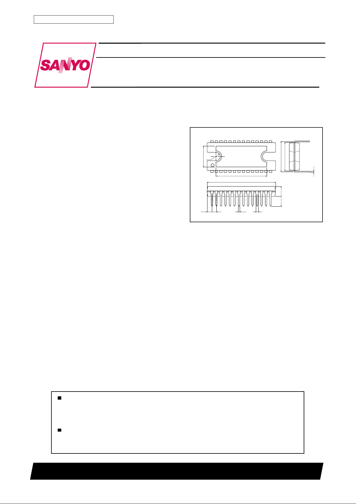
Package Dimensions
unit: mm
3147B-DIP28H
voltage is constant while the current can be set in
15 steps, allowing drive of motors ranging from 12 phase exciter types to 4W 1-2 phase exciter
types. The current decay pattern can also be
selected (SLOW DECAY, FAST DECAY, MIX
DECAY) to increase the decay of regenerative
current at chopping OFF, thereby improving
response characteristics. This is especially useful
for carriage and paper feed stepping motors in
printers and similar applications where highprecision control and low vibrations are required.
Features
• PWM current control (fixed OFF time)
• Load current digital selector (1-2, W1-2, 2W1-2, 4W1-2 phase exciter drive possible)
• Selectable current decay pattern (SLOW DECAY, FAST DECAY, MIX DECAY)
• Simultaneous ON prevention function (feedthrough current prevention)
• Noise canceler
• Built-in thermal shutdown circuit
• Built-in logic low-voltage OFF circuit
[LB1847]
SANYO : DIP28H
Any and all SANYO products described or contained herein do not have specifications that can handle
applications that require extremely high levels of reliability, such as life-support systems, aircraft's
control systems, or other applications whose failure can be reasonably expected to result in serious
physical and/or material damage. Consult with your SANYO representative nearest you before using
any SANYO products described or contained herein in such applications.
SANYO assumes no responsibility for equipment failures that result from using products at values that
exceed, even momentarily, rated values (such as maximum ratings, operating condition ranges, or other
parameters) listed in products specifications of any and all SANYO products described or contained
herein.
SANYO Electric Co., Ltd. Semiconductor Business Headquarters
TOKYO OFFICE Tokyo Bldg., 1-10, 1 Chome, Ueno, Taito-ku, TOKYO, 110-8534 JAPAN
11499RM(KI)
No. 5982-1/16
Page 2

LB1847
Specifications
Maximum Ratings at Ta = 25°C
Parameter Symbol Conditions Ratings Unit
Motor supply voltage 50 V
Output peak current 1.75 A
Output continuous current 1.5 A
Logic supply voltage 7.0 V
Logic input voltage range V
Emitter output voltage 1.0 V
Allowable power dissipation Pd max Ta=25°C 3.0 W
Operating temperature range Topr °C
Storage temperature range Tstg °C
Allowable Operating Ranges at Ta = 25°C
Parameter Symbol Conditions Ratings Unit
Motor supply voltage range 10 to 45 V
Logic supply voltage range 4.75 to 5.25 V
Reference voltage range 0.0 to 3.0 V
V
BB
I
OPEAK
IO max
V
CC
V
IN
V
E
V
BB
V
CC
V
REF
tW≤20 µs
–0.3 to V
CC
With heat sink 20 W
–20 to +85
–55 to +150
25
Pd max – Ta
With an arbitrary large heat sink
20
15
10
5
IC only
Allowable power dissipation, Pdmax – W
0
0–20 20 40 60 80 100
3.0
Ambient temperature, Ta – ˚C
20.0
10.4
1.56
No. 5982-2/16
Page 3
LB1847
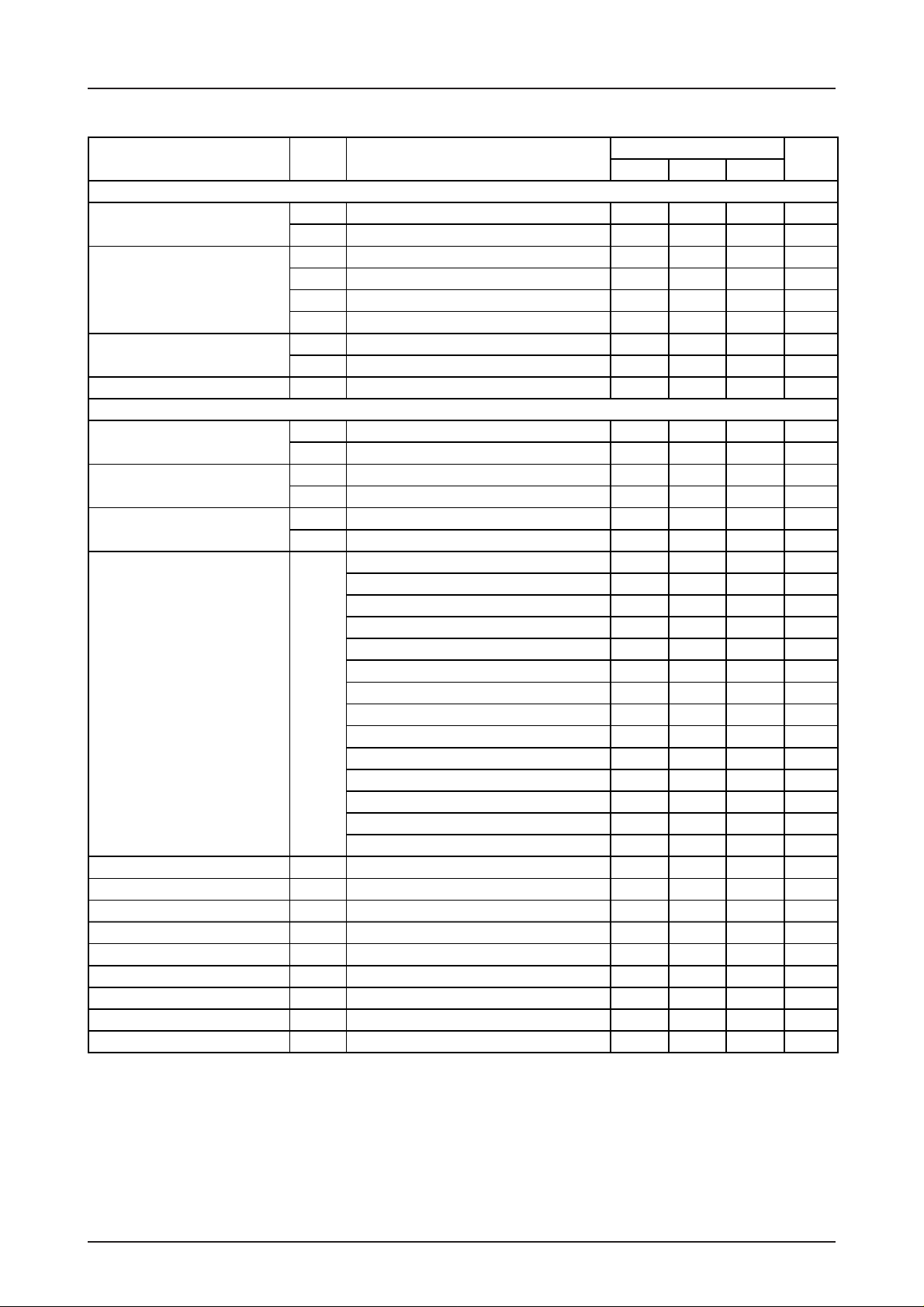
Electrical Characteristics at Ta = 25°C, V
Parameter Symbol Conditions
= 45V, V
BB
= 5V, V
CC
REF
= 1.52V
Ratings
min typ max
[Output Block]
Output stage supply voltage 2.3 3.5 5.0 mA
Output saturation voltage 1.2 1.6 V
Output leak current 50 µA
Output sustain voltage 45 V
I
BB ON
IBB
OFF
VO(sat)1
(sat)2
V
O
V
(sat)3
O
VO(sat)4
IO(leak)1
IO(leak)2
V
SUS
IO=+1.0A, sink
I
=+1.5A, sink
O
I
=–1.0A, source
O
IO=–1.5A, source
VO=VBB, sink
VO=0V, source
L=15 mH, IO=1.5A, Guaranteed design value
0.5 0.8 1.1 mA
1.5 1.9 V
1.9 2.2 V
2.2 2.4 V
–50 µA
[Logic Block]
Logic supply voltage 19.5 26 36.5 mA
Input voltage 3.2 V
Input current 100 µA
Sensing voltage 0.470 0.525 V
Reference current –0.5 µA
CR pin current CR=1.0V –4.6 –1.0 mA
MD pin current MD=1.0V, CR=4.0V –5.0 µA
DECAY pin current Low –10 µA
DECAY pin current High 5 µA
I
CC ON
I
CC OFF
V
IH
V
I
IH
I
IL
V
E
I
REF
I
CR
I
MD
I
DECL
I
DECH
I4=3.2V, I3=3.2V, I2=3.2V, I1=3.2V
ENABLE=3.2V 10.5 15 19.5 mA
IL
VIH=3.2V
VIL=0.8V
I4=3.2V, I3=3.2V, I2=3.2V, I1=3.2V
I
=3.2V, I3=3.2V, I2=3.2V, I1=0.8V
4
I4=3.2V, I3=3.2V, I2=0.8V, I1=3.2V
=3.2V, I3=3.2V, I2=0.8V, I1=0.8V
I
4
I
=3.2V, I3=0.8V, I2=3.2V, I1=3.2V
4
I4=3.2V, I3=0.8V, I2=3.2V, I1=0.8V
I4=3.2V, I3=0.8V, I2=0.8V, I1=3.2V
=3.2V, I3=0.8V, I2=0.8V, I1=0.8V
I
4
=0.8V, I3=3.2V, I2=3.2V, I1=3.2V
I
4
I4=0.8V, I3=3.2V, I2=3.2V, I1=0.8V
I4=0.8V, I3=3.2V, I2=0.8V, I1=3.2V
I4=0.8V, I3=3.2V, I2=0.8V, I1=0.8V
I4=0.8V, I3=0.8V, I2=3.2V, I1=3.2V
=0.8V, I3=0.8V, I2=3.2V, I1=0.8V
I
4
V
=1.5V
REF
V
=0.8V
DEC
V
=3.2V
DEC
–10 µA
0.50
0.445 0.48 0.505 V
0.425 0.46 0.485 V
0.410 0.43 0.465 V
0.385 0.41 0.435 V
0.365 0.39 0.415 V
0.345 0.37 0.385 V
0.325 0.35 0.365 V
0.280 0.3 0.325 V
0.30
0.240 0.26 0.285 V
0.195 0.22 0.235 V
0.155 0.17 0.190 V
0.115 0.13 0.145 V
0.075 0.09 V
0.8 V
0.190
0.100
Thermal shutdown temperature TSD 170 °C
Logic ON voltage 3.35 3.65 3.95 V
Logic OFF voltage 3.20 3.50 3.80 V
L
hysteresis width
VSD
L
∆L
L
VSD
VSD
VSD
1
2
0.065 0.15 0.23 V
Unit
No. 5982-3/16
Page 4
LB1847
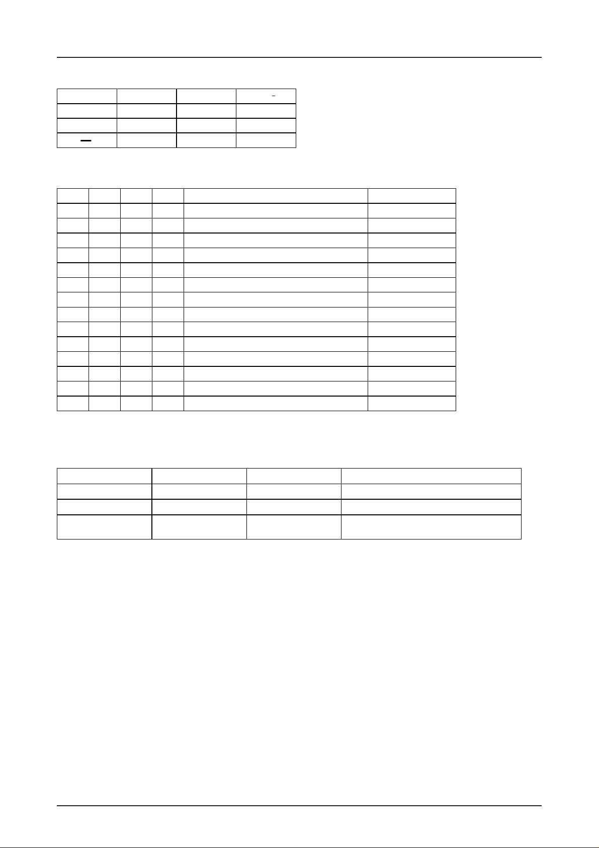
Truth table
PHASE ENABLE
HLHL
LLLH
HOFFOFF
Set current truth table
I
IA4IA3
1111 100
1110 95.65
1101 91.30
1100 86.95
1011 82.61
1010 78.26
1001 73.91
1000 69.56
0111 60.87
0110 52.17
0101 43.48
0100 34.78
0011 26.08
0010 17.39
* Current ratio (%) is the calculated set current value.
2
I
A
A
1
11.5/11.5 X V
11.0/11.5 X V
10.5/11.5 X V
10.0/11.5 X V
9.5/11.5 X V
9.0/11.5 X V
8.5/11.5 X V
8.0/11.5 X V
7.0/11.5 X V
6.0/11.5 X V
5.0/11.5 X V
4.0/11.5 X V
3.0/11.5 X V
2.0/11.5 X V
OUT
A
OUT
A
Set current Iout Current ratio (%)
/3.04RE=Iout
REF
/3.04RE=Iout
REF
/3.04RE=Iout
REF
/3.04RE=Iout
REF
/3.04RE=Iout
REF
/3.04RE=Iout
REF
/3.04RE=Iout
REF
/3.04RE=Iout
REF
/3.04RE=Iout
REF
/3.04RE=Iout
REF
/3.04RE=Iout
REF
/3.04RE=Iout
REF
/3.04RE=Iout
REF
/3.04RE=Iout
REF
Current decay switching truth table
Current decay mode DECAY pin MD pin Output chopping
SLOW DECAY H L Top-side chopping
FAST DECAY L L Dual-side chopping
MIX DECAY
L
4V to 1.5V input
voltage setting
CR voltage > MD : dual-side chopping
CR voltage < MD : top-side chopping
No. 5982-4/16
Page 5

LB1847
Pin function
Pin number Pin name Function description
1
2 Output set current reference supply pin
13 Setting voltage range: 0V to 3V
3 CR1
12 CR2
4E1
11 E2
5 DECAY1 SLOW mode/FAST mode selector pin
10 DECAY2 SLOW DECAY: H
6
7
8
9
14 Output stage supply voltage pin
15 GND Ground pin
27 PHASE1
16 PHASE2
26 ENABLE1
17 ENABLE2
22, 23
24, 25 Output set current digital input pin
21, 20 15-stage voltage setting
19, 18
28 Logic block supply voltage pin
M D
V
REF
V
REF
OUT
OUT
OUT
OUT
V
BB
IA4, IA3
I
2, IA1
A
4, IB3
I
B
I
2, IB1
B
V
CC
Sets the OFF time for FAST mode and SLOW mode in MIX DECAY
Setting input range: 4V to 1.5V
1
2
Output OFF time setting pin for switching operation
Pin for controlling the set current with sensing resistor RE
FAST DECAY: L
A
A
B
B
Output pin
Output phase selector input pin
Output ON/OFF setting input pin
Pin Assignment
VCCPHASE1
1282273264
MD
1
REF
V
1
2
3
4
4
3
2
A
ENABLE1
I
A
A
A
B
I
I
I
B
I
I
1
B
B
I
I
ENABLE2
2552462372282192010191118121713161415
LB1847
CR1
E1
DECAY1
A
OUT
OUTAOUTBOUT
B
DECAY2
E2
CR2
PHASE2
2
REF
V
A11312
GND
BB
V
Top view
No. 5982-5/16
Page 6
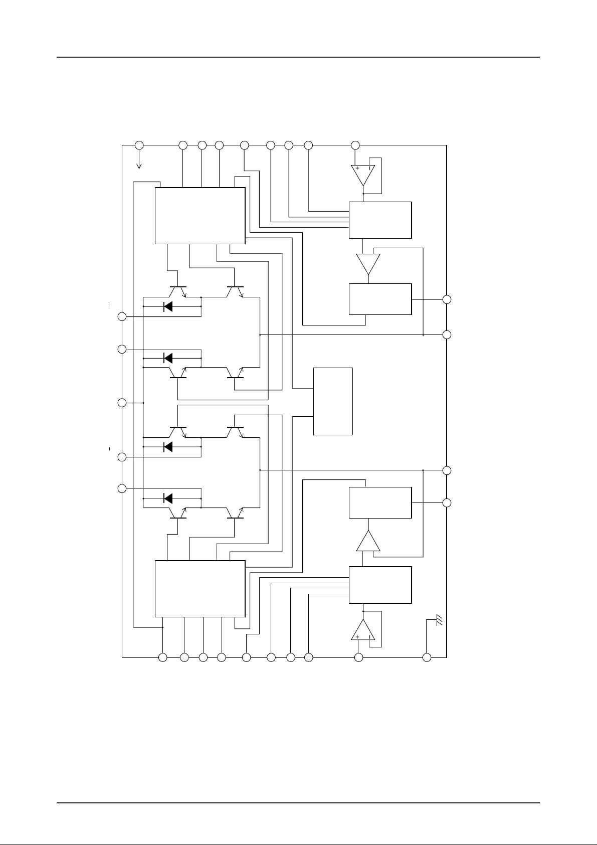
Block diagram
Control logic
circuit
Thermal shutdown
circuit
Control logic
circuit
Current
selector
circuit
Current
selector
circuit
One-shot
multi-
blanking
time
One-shot
multi-
blanking
time
MD
PHASE1
DECAY1
ENABLE1
I
A
1
I
A
2
I
A
3
I
A
4
V
REF
1
GND
V
CC
OUT
B
OUT
B
V
BB
OUT
A
OUT
A
PHASE2
DECAY2
ENABLE2
I
B
1
I
B
2
I
B
3
I
B
4
V
REF
2
CR1
E1
E2
CR2
A11311
LB1847
No. 5982-6/16
Page 7
LB1847
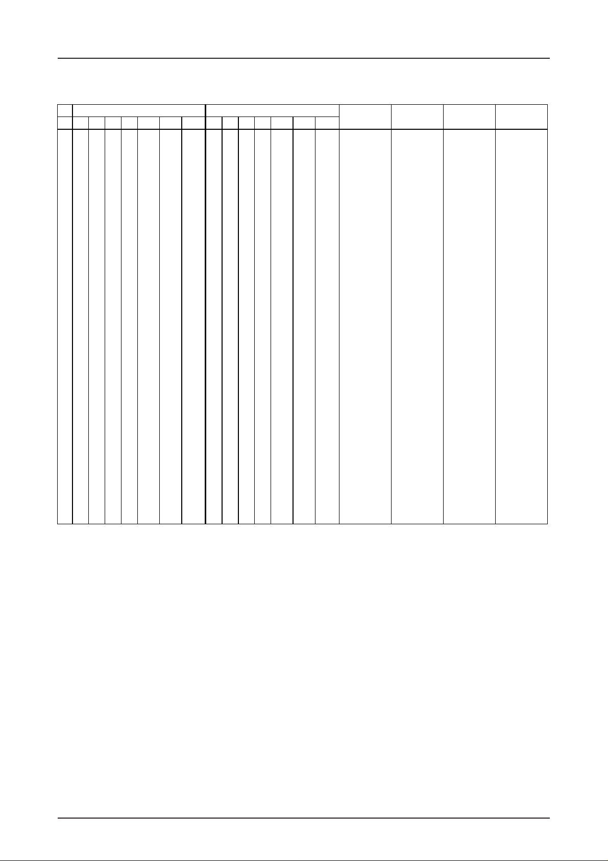
Sequence table
Phase A Phase B
No. IA4 IA3 IA2 IA1 ENA1 PHA1 Iout IB4 IB3 IB2 IB1 ENA1 PHA1 Iout
01111 0 0100% 0010 1 0%
11111 0 0100 0010 0 017.39
21111 0 0100 0011 0 026.08
31110 0 096.650100 0 034.78
41101 0 091.300101 0 043.48
51100 0 086.950110 0 052.17
61011 0 082.610111 0 060.87
71010 0 078.261000 0 069.56
81001 0 073.911001 0 073.91
91000 0 069.561010 0 078.26
100111 0 060.871011 0 082.61
110110 0 052.171100 0 086.95
120101 0 043.481101 0 091.30
130100 0 034.781110 0 096.65
140011 0 026.081111 0 0100
150010 0 017.391111 0 0100
160001 1 * 0 1111 0 0100
170010 0 117.391111 0 0100
180011 0 126.081111 0 0100
190100 0 134.781110 0 095.65
200101 0 143.481101 0 091.30
210110 0 152.171100 0 086.95
220111 0 160.871011 0 082.61
231000 0 169.561010 0 078.26
241001 0 173.911001 0 073.91
251010 0 178.261000 0 069.56
261011 0 182.610111 0 060.87
271100 0 186.950110 0 052.17
281101 0 191.300101 0 043.48
291110 0 195.650100 0 034.78
301111 0 1100 0011 0 026.08
311111 0 1100 0010 0 017.39
* : Iout percentage (%) is the calculated setting value.
*
Phase 1-2
Phase W1-2 Phase 2W1-2 Phase 4W1-2
√√√√
√
√√
√
√√√
√
√√
√
√√√√
√
√√
√
√√√
√
√√
√
√√√√
√
√√
√
√√√
√
√√
√
√√√√
√
√√
√
√√√
√
√√
√
No. 5982-7/16
Page 8
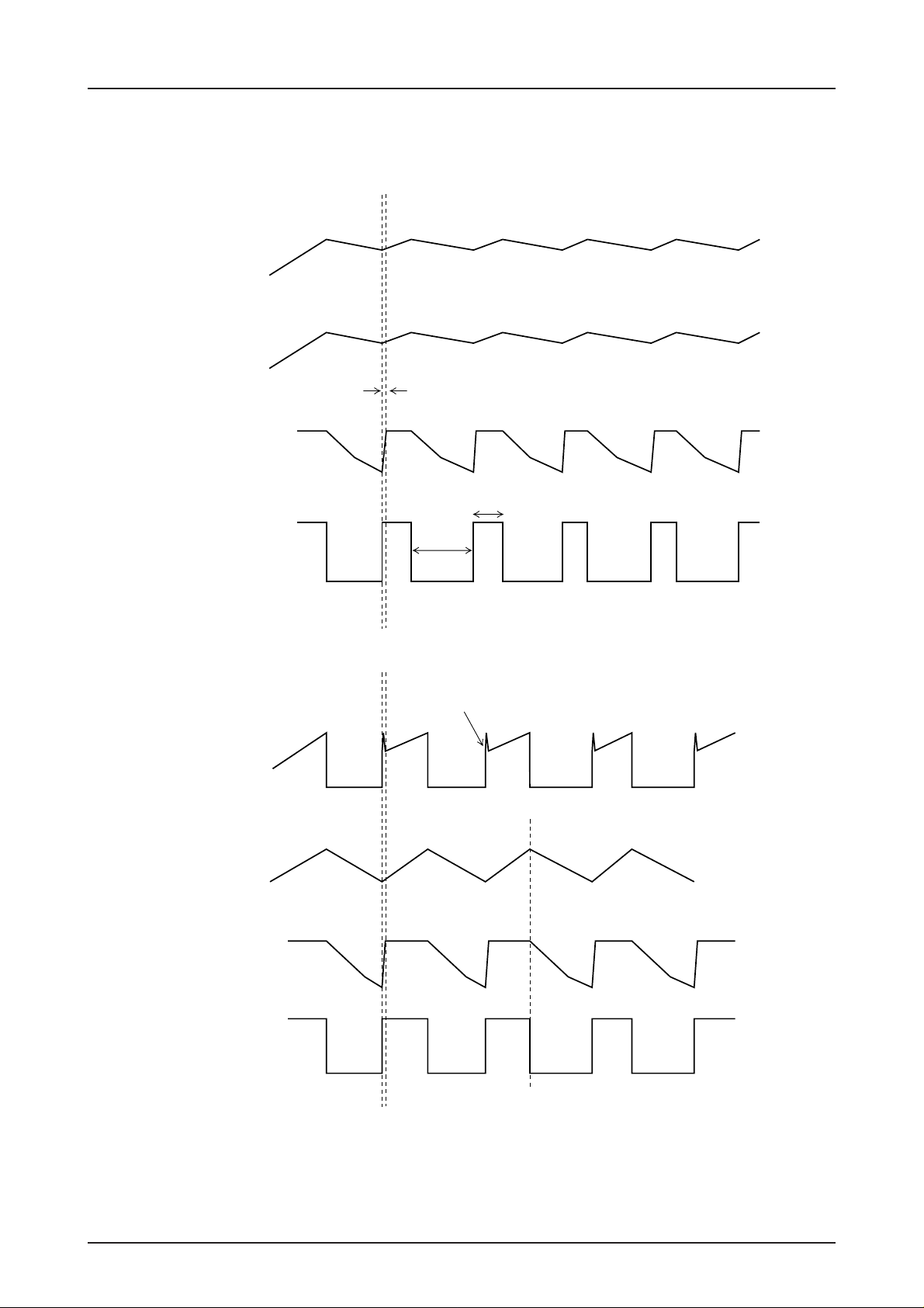
Switch timing chart during PWM drive
SLOW DECAY(top-side chopping)
DECAY pin : High
Output pin
RC pin
E pin
MD pin : Low
t
n
LB1847
Output oin
FAST DECAY
DECAY pin : High
Output pin
RC pin
E pin
MD pin : Low
Switching waveform
Noise spike
A11313
Output pin
Switching waveform
A11314
No. 5982-8/16
Page 9
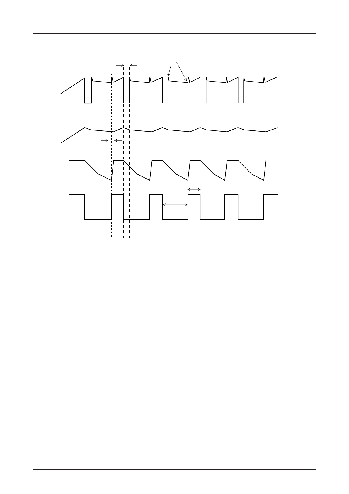
MIX DECAY
E pin
Output pin
RC pin
LB1847
Noise spike
t
m
t
n
t
on
Output pin
off
t
Switching waveform
t
on
: Output ON time
t
off
: Output OFF time
t
m
: FAST DECAY time in MIX DECAY mode
t
n
: Noise cancelling time
MIX DECAY logic setting
DECAY pin : L
MD pin : 1.5V to 4.0V voltage setting
CR voltage and MD pin voltage are compared to select dual-side chopping
or top-side chopping.
CR voltage > MD pin voltage: dual-side chopping
CR voltage < MD pin voltage: top-side choppi
A11315
No. 5982-9/16
Page 10
LB1847
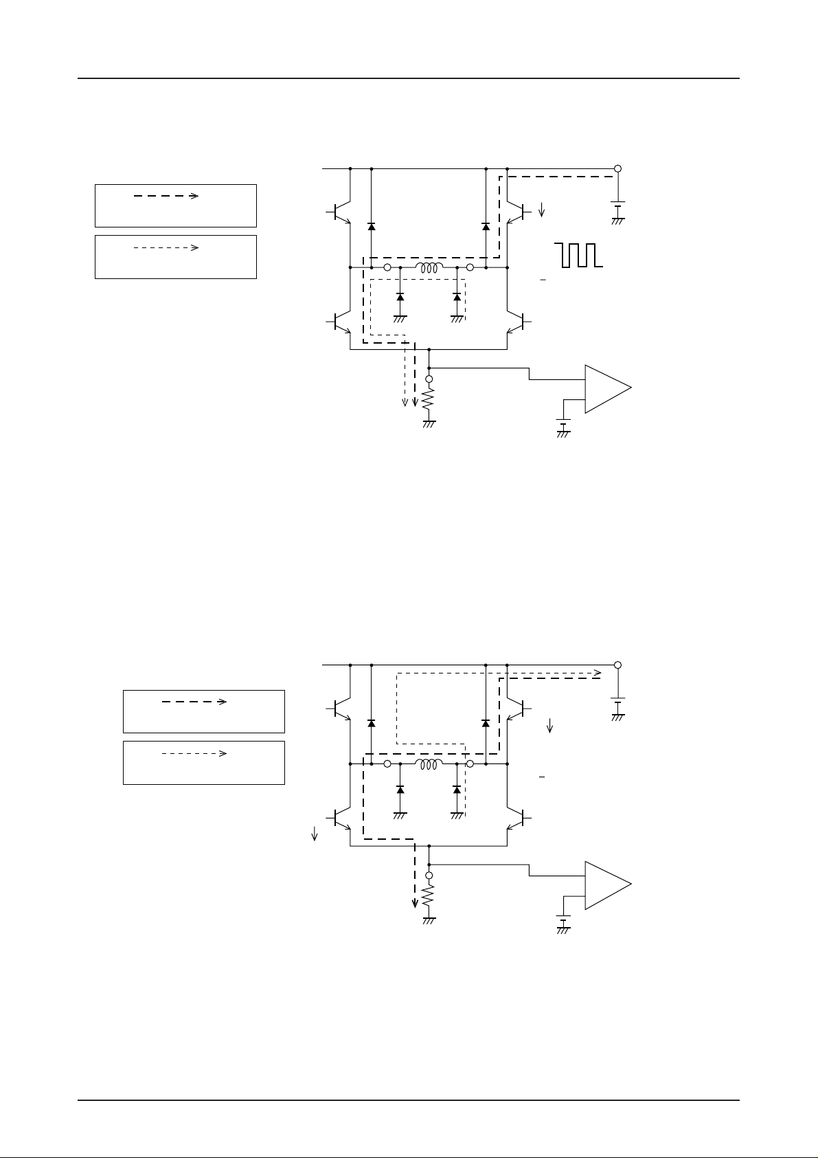
SLOW DECAY current path
Regenerative current during top-side transistor switching operation
ON
V
BB
Current path at output ON
Regenerative circuit
when top-side transistor is OFF
Current path in FAST DECAY mode
OUT
ON
Constant
OFF
A
SBD
SBD
Re
A
OUT
Sensing voltage comparator
A11316
Current path at output ON
Current path in FAST DECAY mode
OUT
ON
OFF
V
BB
ON
OFF
A
SBD
SBD
Re
OUT
A
Sensing voltage comparator
A11317
No. 5982-10/16
Page 11
LB1847
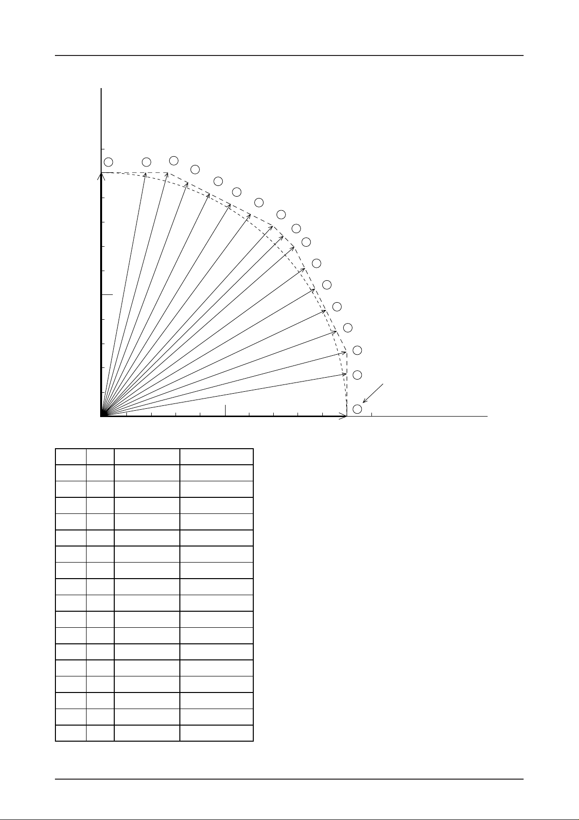
Composite spectrum of set current (1 step normalized to 90°)
Phase B
I
OUT
16
14
15
13
12
11
10
9
8
7
6
5
4
3
No. θ Rotation angle Composite spectrum
0
θ0
1
θ1
2
θ2
3
θ3
4
θ4
5
θ5
6
θ6
7
θ7
8
θ8
9
θ9
10
θ10
11
θ11
12
θ12
13
θ13
14
θ14
15
θ15
16
θ16
0° 100.0
9.87° 101.5
14.6° 103.35
20.0° 101.78
25.5° 101.12
30.96° 101.4
36.38° 102.61
41.63° 104.7
45.0° 104.5
48.37° 104.7
53.62° 102.61
59.04° 101.4
64.5° 101.12
70.0° 101.78
75.4° 103.35
80.13° 101.5
90.0° 100.0
2
1
0
Phase A
Sequence No.
OUT
I
A11318
* Rotation angle and composite spectrum are calculated values.
No. 5982-11/16
Page 12
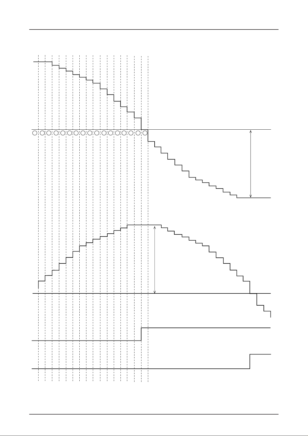
Set current waveform model
0 1 2 3 4 5 6 7 8 9 10 11 12 13 14 15 16
LB1847
Phase A
I
OUT
I
OUT
PHASE1
Phase B
PHASE2
A11319
No. 5982-12/16
Page 13
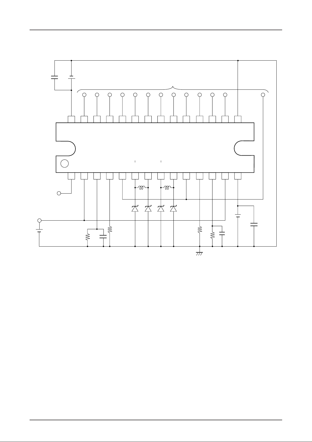
Sample Application Circuit
LB1847
10 µF
1.5V to 4.0V
voltage setting
1.5V
5V
Logic input
28 27 26 25 24 23 22 21 20 19 18 17 16 15
1
2
3
4
4
3
2
V
CC
PHASE1
I
ENABLE1
A
A
A
A
B
I
I
I
B
I
I
1
B
B
I
I
ENABLE2
GND
PHASE2
LB1847
1
REF
MD
V
CR1
E1
1234567891011121314
SBD
0.51Ω
15 kΩ
470 pF
DECAY1
A
OUTAOUTBOUTBDECAY2E2CR2
OUT
LL
SBD
SBD
SBD
0.51Ω
15 kΩ
2
REF
V
470 pF
BB
V
42V
47 µF
A11320
Notes on Usage
1. External diodes
Because this IC uses top-side transistor switching in SLOW DECAY mode and dual-side transistor switching in FAST DECAY
mode, it requires external diodes between the OUT pins and ground, for the regenerative current during switching OFF . Use Schottky
barrier diodes with low VF.
2. V
REF
pin
Because the V
range is 0 to 3.0V.
3. GND pin
The ground circuit for this IC must be designed so as to allow for high-current switching. Blocks where high current flows must use
low-impedance patterns and must be removed from small-signal lines. Especially the ground connection for the sensing resistor RE
at pin E, and the ground connection for the Schottky barrier diodes should be in close proximity to the IC ground.
The capacitors between VCC and ground, and VBB and ground should be placed close to the V
REF
pin serves for input of the set current reference voltage, precautions against noise must be taken. The input voltage
CC
and V
BB
pins, respectively.
No. 5982-13/16
Page 14
LB1847
4. Simultaneous ON prevention function
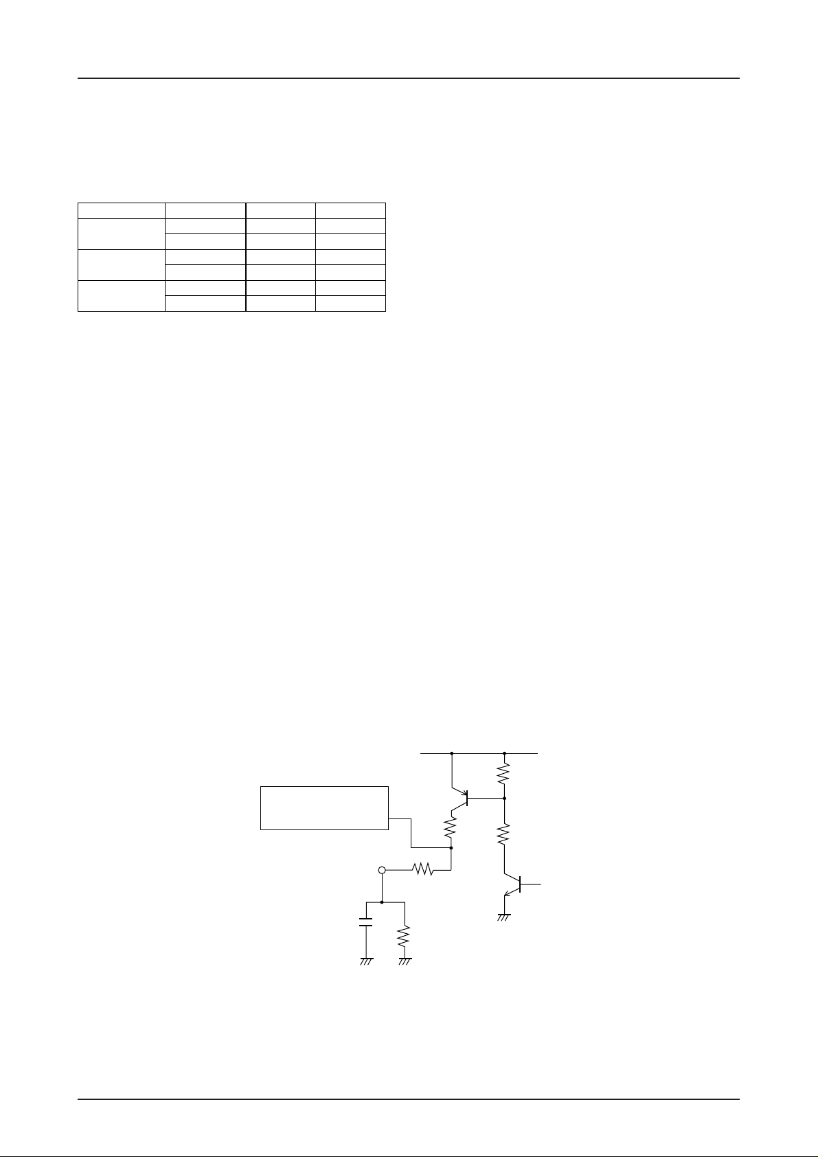
This IC incorporates a circuit to prevent feedthrough current when phase switching. For reference, the output ON and OFF delay
times at PHASE and ENABLE switching are given below.
Reference data * typical value
Sink side Source side
PHASE switching ON delay time 1.9 µs 2.2 µs
(Low -> Hi)
PHASE switching ON delay time 1.4 µs 1.7 µs
(Hi -> Low) OFF delay time 0.9 µs 1.35 µs
ENABLE switching ON delay time 2.15 µs 2.75 µs
5. Noise canceler
This IC has a noise canceling function to prevent malfunction due to noise spikes generated when switching ON. The noise cancel
time tn is determined by internal resistance of the CR pin and the constant of the externally connected CR components. The constant
also determines the switching OFF time.
Figure 1 shows the internal configuration at the CR pin, and Figure 2 the CR pin constant setting range.
Equation when logic voltage VCC = 5 V
CR pin voltage E1 = V
Noise cancel time t
Switching OFF time t
Internal resistance at CR pin : R1 = 1 kΩ, R2 = 300Ω (typ.)
OFF delay time 0.8 µs 1.8 µs
OFF delay time 1.2 µs 5.8 µs
CC
• R/(R1+R2+R) [V]
.
n
(R1+R2) • C • 1n {(E1-1.5)/(E1-4.0)} [s]
=
.
.
=
off
–R • C • 1n (1.5/E1) [s]
.
*The CR constant setting range in Figure 2 on page 15 is given for reference. It applies to a switching OFF time in the range from 8
to 100 µs. The switching time can also be made higher than 100 µs. However, a capacitor value of more than several thousand pF
will result in longer noise canceling time, which can cause the output current to become higher than the set current. The longer
switching OFF time results in higher output current ripple, causing a drop in average current and rotation efficiency. When keeping
the switching OFF time within 100 µs, it is recommended to stay within the CR constant range shown in Figure 2.
Internal configuration at CR pin
V
CC
line
One-shot multi-blanking
time circuit
CR pin
E1
R1R21 kΩ
300Ω
R:15 kΩC:470 pF
Figure 1
A11321
No. 5982-14/16
Page 15
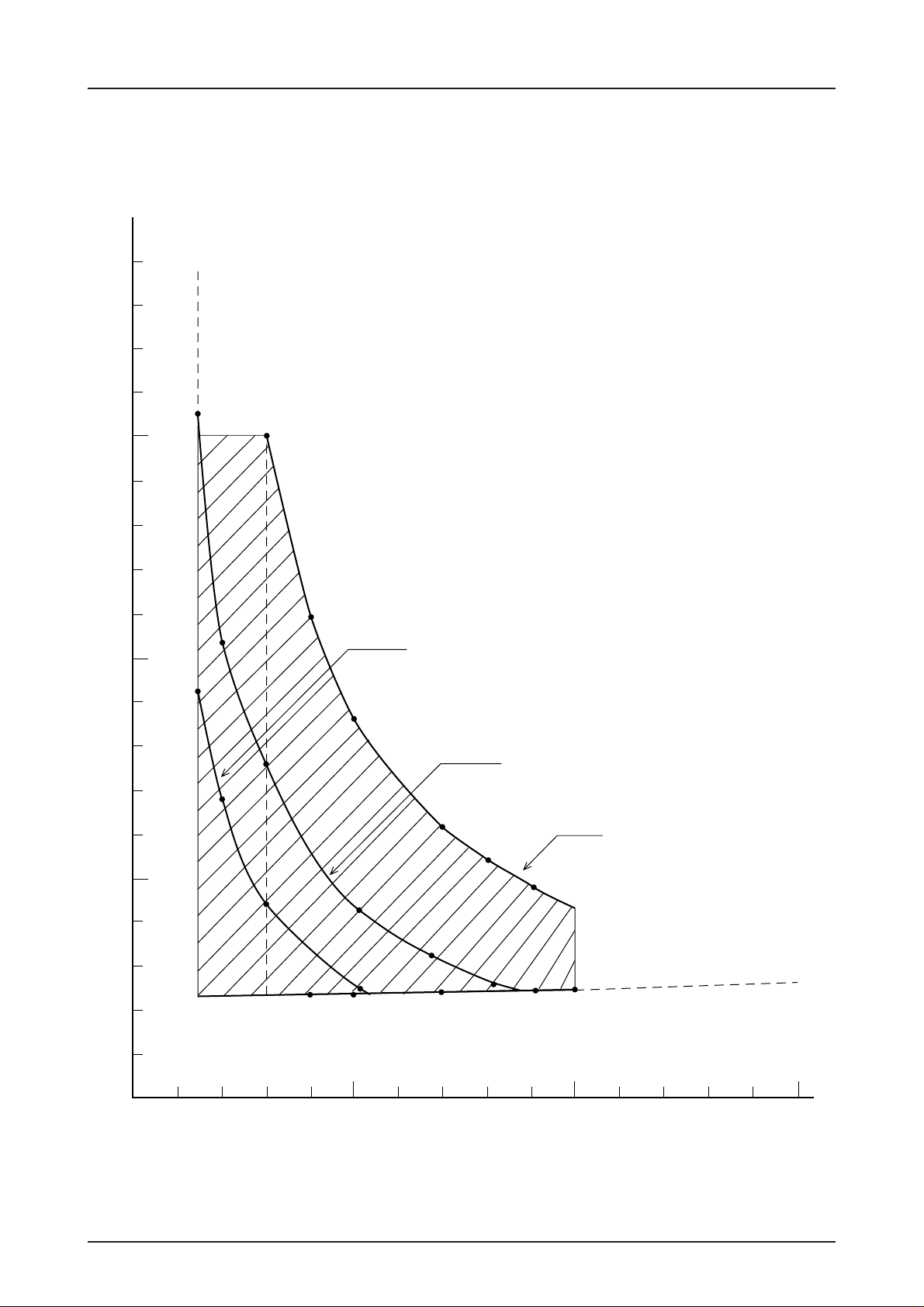
Switching OFF time and CR setting range
(t
time : approx. 8 to 100 µs)
off
C [pF]
3000
LB1847
2000
1000
t
off
time : 30 µs
time : 50 µs
t
off
time : 100 µs
t
off
50k 100k
Figure 2
R [Ω]
A11322
No. 5982-15/16
Page 16
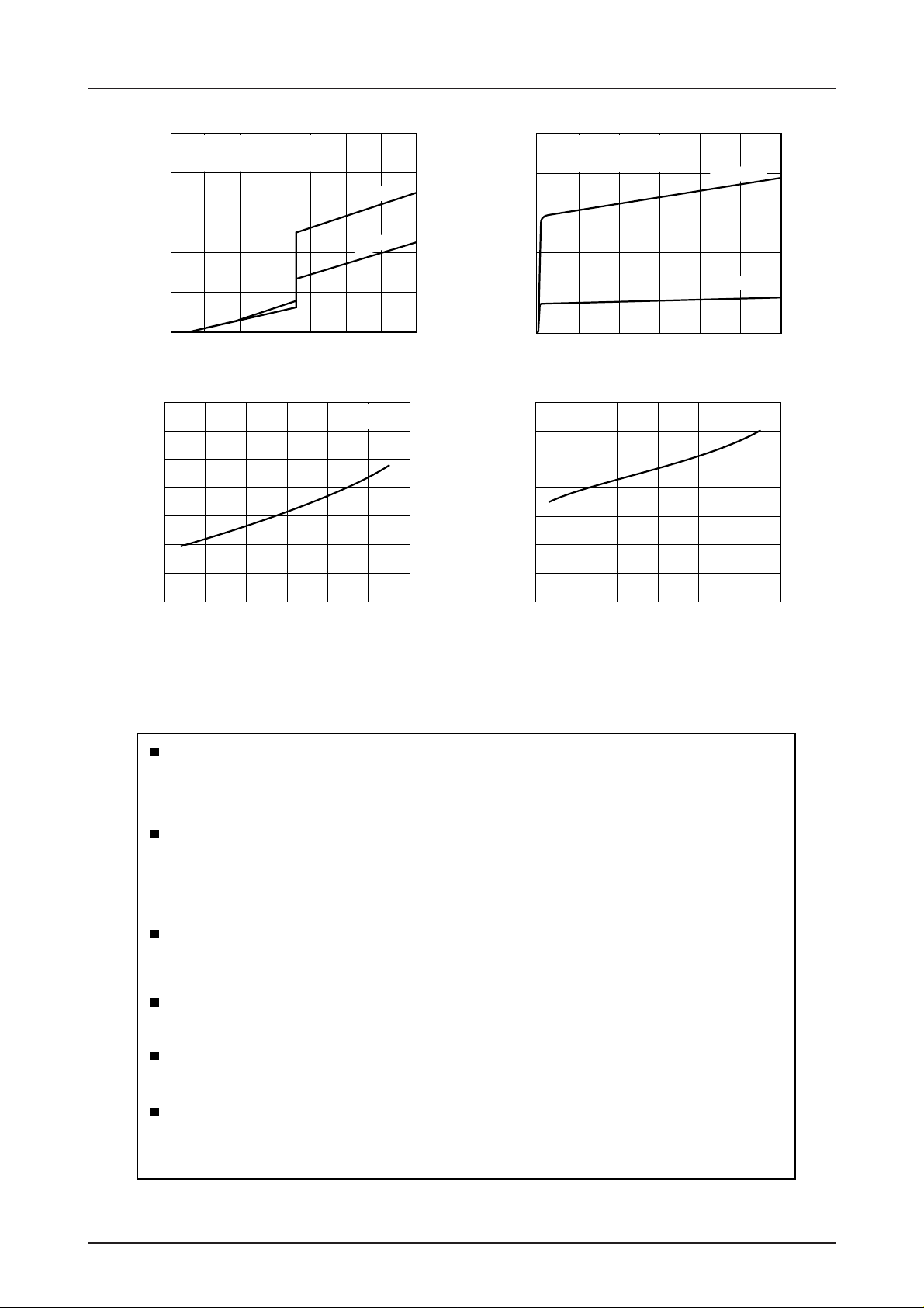
LB1847
50
Input logic voltage: IA1,2,3,4
PHA,ENA=V
typ.
40
CC
Icc – V
cc
– mA
CC
30
20
10
Logic supply current, I
0
01 2 34 5 6
Logic supply voltage, VCC – mV
V
– I
o
– V
(sat)
o
2.8
2.4
2.0
1.6
1.2
0.8
0.4
(sat)
o
Output saturation voltage, V
0
0
1.2 1.60.80.4
Output current, I
o
– A
Output ON
Output OFF
Sink side
[typ.]
2.0 2.4
5
Input logic voltage: IA1,2,3,4
– mA
BB
4
3
2
1
PHA,ENA=V
typ.
CC
IBB – V
BB
Output ON
Output OFF
Output stage supply current, I
7
0
01020304050
60
Output stage supply current voltage, VBB – V
V
– I
o
(sat) – V
o
2.8
2.4
2.0
1.6
1.2
0.8
0.4
(sat)
o
Source side
[typ.]
Output saturation voltage, V
0
0
1.2 1.60.80.4
Output current, Io – A
2.0 2.4
Specifications of any and all SANYO products described or contained herein stipulate the performance,
characteristics, and functions of the described products in the independent state, and are not guarantees
of the performance, characteristics, and functions of the described products as mounted in the customer's
products or equipment. To verify symptoms and states that cannot be evaluated in an independent device,
the customer should always evaluate and test devices mounted in the customer's products or equipment.
SANYO Electric Co., Ltd. strives to supply high-quality high-reliability products. However, any and all
semiconductor products fail with some probability. It is possible that these probabilistic failures could
give rise to accidents or events that could endanger human lives, that could give rise to smoke or fire,
or that could cause damage to other property. When designing equipment, adopt safety measures so
that these kinds of accidents or events cannot occur. Such measures include but are not limited to protective
circuits and error prevention circuits for safe design, redundant design, and structural design.
In the event that any or all SANYO products(including technical data,services) described or
contained herein are controlled under any of applicable local export control laws and regulations,
such products must not be exported without obtaining the export license from the authorities
concerned in accordance with the above law.
No part of this publication may be reproduced or transmitted in any form or by any means, electronic or
mechanical, including photocopying and recording, or any information storage or retrieval system,
or otherwise, without the prior written permission of SANYO Electric Co. , Ltd.
Any and all information described or contained herein are subject to change without notice due to
product/technology improvement, etc. When designing equipment, refer to the "Delivery Specification"
for the SANYO product that you intend to use.
Information (including circuit diagrams and circuit parameters) herein is for example only ; it is not
guaranteed for volume production. SANYO believes information herein is accurate and reliable, but
no guarantees are made or implied regarding its use or any infringements of intellectual property rights
or other rights of third parties.
This catalog provides information as of January, 1999. Specifications and information herein are subject to change
without notice.
No. 5982-16/16
PS
 Loading...