

Page 1

Ordering number: EN 4385B
Monolithic Digital IC
LB1843V
Low-saturation, current-controlled
bidirectional motor driver
Overview
The LB1843V is a low-saturation bidirectional motor driver
with output current limitation and detection functions. This
design is ideal for controlling the loading motor in a video
camera.
Package Dimensions
unit : mm
3179A-SSOP20
[LB1843V]
Features
.
Output current limiter and detector built in
.
Low-saturation voltage bidirectional bridge circuit built in:
V
sat = 0.40 V typ. at 400 mA
O
.
Practically no current drain (0.1 µA or less) in standby mode
.
Input-linked reference voltage built in
.
Thermal shutdown circuit built in
.
Requires little space, since few external components are
needed and the IC is contained in a small SSOP-20 package
SANYO : SSOP20
Specifications
Absolute Maximum Ratings at Ta = 25°C
Parameter Symbol Conditions Ratings Unit
Maximum supply voltage V
Maximum output current Im max 800 mA
Applied input voltage V
Allowable power dissipation Pd max With board ( 50 × 35 × 1.6 mm
Operating temperature Topr –20 to +80 °C
Storage temperature Tstg –40 to +150 °C
max 10.5 V
CC
IN
3
) 800 mW
–0.3 to +10 V
Allowable Operating Ranges at Ta = 25°C
Parameter Symbol Conditions Ratings Unit
Supply voltage V
V
voltage V
M
High-level input voltage V
Low-level input voltage V
LIR input voltage V
Output current limitation I
CC
M
IH
IL
LIR
limit
3.0 to 9.0 V
2.2 to V
3.0 to 9.0 V
–0.3 to +0.7 V
0.5 to VCC–1.0 V
50 to 350 mA
SANYO Electric Co.,Ltd. Semiconductor Bussiness Headquarters
TOKYO OFFICE Tokyo Bldg., 1-10, 1 Chome, Ueno, Taito-ku, TOKYO, 110 JAPAN
O3096HA(II) No.4385-1/6
CC
V
Page 2

LB1843V
Electrical Characteristics at Ta = 25°C, VCC= 7.2 V
Parameter Symbol Conditions min typ max Unit
0 During standby 0.1 10 µA
I
CC
I
Supply current
Output saturation voltage
Reference voltage Vref I
Set output current I
Input current I
RD saturation voltage V
Output current limit is determined by the following equation (Rfis the sensing resistance between VCCand VM):
I
limit=VLIR
The input range for V
/10Rf(A)
LIR
is 0.5 to VCC–1.0 (V)
1 During bidirectional operation, no load 9 13 mA
CC
I
2 During braking 12 18 mA
CC
Vsat1 I
Vsat2 I
limit
IN
sat IO= 1 mA 0.3 V
RD
= 200 mA (upper side + lower side) 0.20 0.30 V
O
= 400 mA (upper side + lower side) 0.40 0.60 V
O
ref = 1 mA 1.85 2.0 2.15 V
V
Resistance between VCCand VM=1Ω,
when LIR = 2 V
VIN= 5 V 90 150 µA
165 185 205 mA
Pd max – Ta
Specified board (50 × 35 × 1.6 mm3glass epoxy)
Allowable power dissipation, Pd max – mW
Ambient temperature, Ta – °C
No.4385-2/6
Page 3
LB1843V
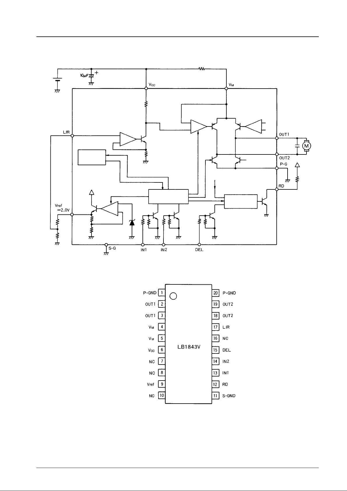
Block Diagram and Sample Application Ciruit
VCC= 3 to 10.5 V
Thermal
shut down
Decoder
Rf= 0.47 to 2 Ω
Limit detection
0.001 µF
to 0.01 µF
Pin Assignment
.
Notes:
Connect both VMpins
(motor power supply/sensing pins).
.
Connect both P-GND pins
(motor power supply GND pins).
.
Connect S-GND (control power
supply GND pin) to the
microcontroller’s GND.
Top view
No.4385-3/6
Page 4
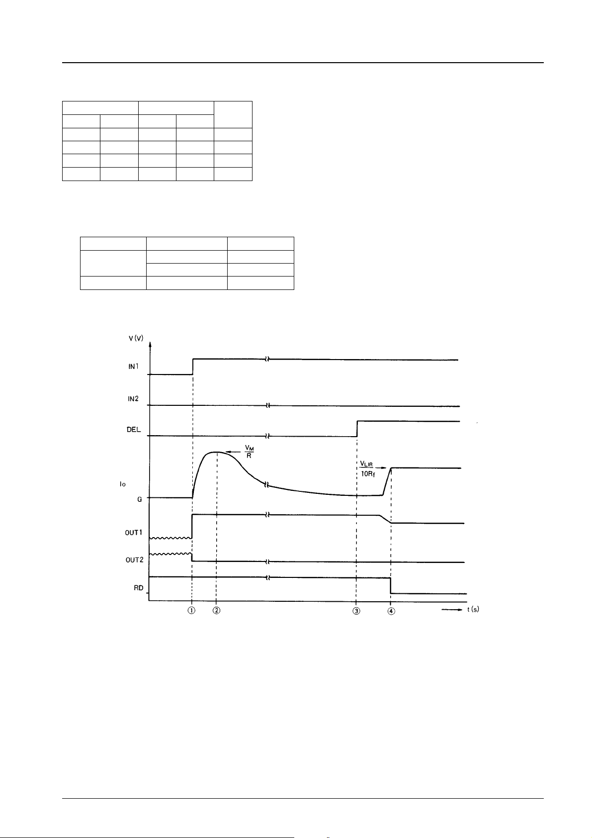
Truth Table
LB1843V
Input Output
IN1 IN2 OUT1 OUT2
L L off off Standby
HLHLForward
LHLHReverse
H H L L Brake
Mode
Output Current Limitation and Detector Output
DEL OUT output RD
H
L Saturated Off
Limit L
Non-limit Off
Sample Application Timing Chart
Sample application timing chart
1 Connect a DC motor (R
=RΩ) between OUT1 and OUT2, and with the RD pin pulled up, input a forward rotation signal
L
(IN1 = high, IN2 = low).
Because the output is used in the saturated state at startup, set the DEL input to low.
2 The DC motor starts up, and the startup current (I
ST=VM
/R) flows to the motor.
3 The DC motor rotates in the normal state. At this point, set the DEL input to high.
4 If the DC motor locks, the motor current I
increases to the point of I
M
limit
(= V
/(10Rf)), the output current limiter operates
LIR
to limit the output current. At the same time, RD is output low from the set current detection circuit.
No.4385-4/6
Page 5
LB1843V
Reference voltage (Vref)
The Vref output is linked to the input; if either IN1 or IN2 is high, the reference voltage is output.
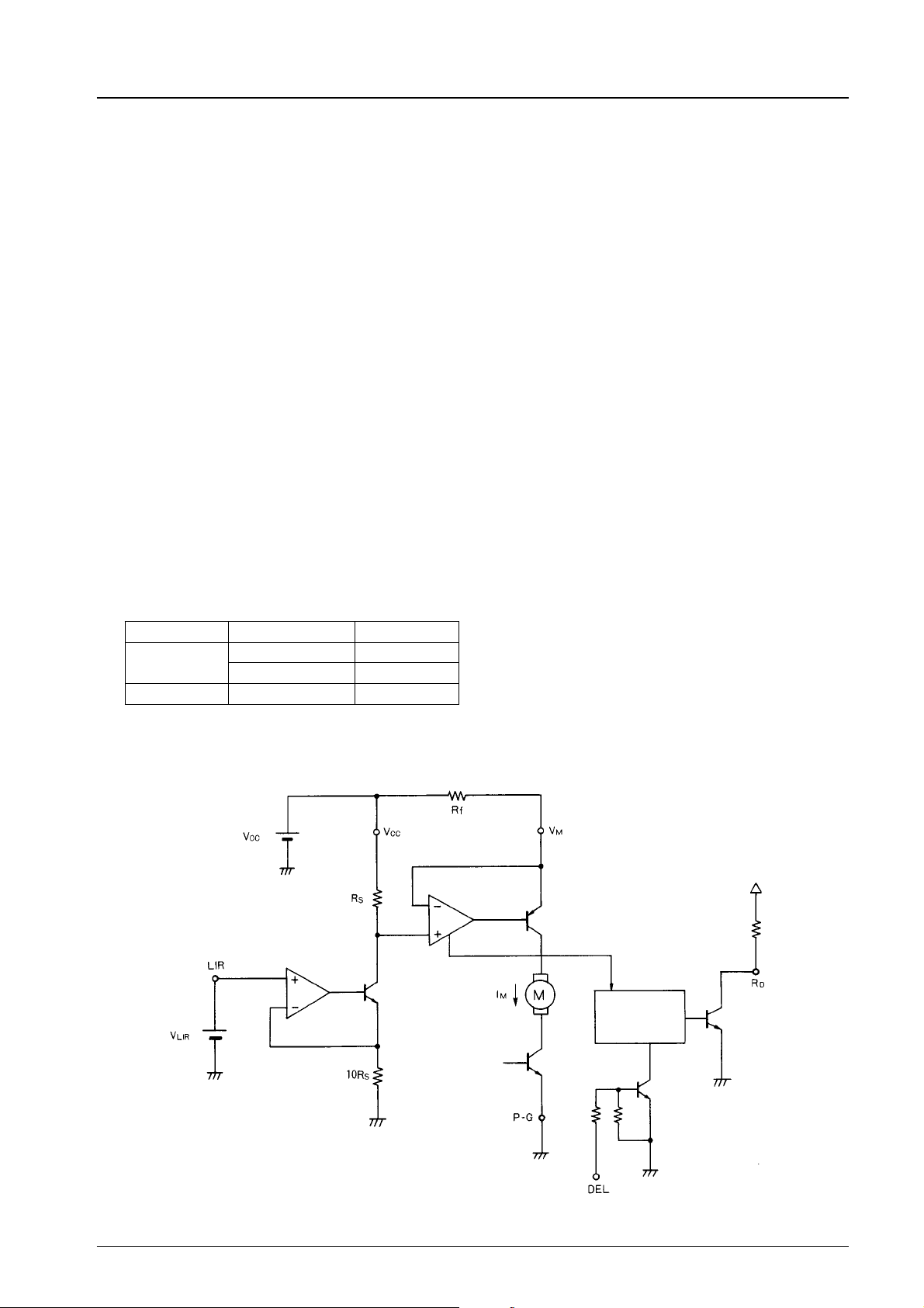
Output current limiter
The schematic for the output current limiter is shown below.
The output set current is set according to the reference voltage V
voltage is generated at both ends of R
in the diagram; this voltage is input on the positive (+) side of the current setting
S
amplifier.
The motor current I
generates voltage equal to (IM× Rf) at both ends of the external resistor Rf. This voltage is input to the
M
negative (–) side of the same amplifier, and the differential amplifier functions and the output transistors are driven so that these
inputs become equal.
The set current value in this instance is determined by the following equation:
I
limit=VLIR
/(10Rf) [A]
Set current detector
(1) When DEL = high
If the motor current I
has not reached the set current I
M
limit
greater than the input voltage on the positive (+) side. As a result, the drive current increases and the output PNP transistors
reach the saturation state. If this state is detected, the detection signal is sent to the set current detector, and the RD output
goes high.
If the motor current I
reaches the set current I
M
, the output PNP transistor enters the controlled state, and the RD output
limit
goes low.
applied to the LIR pin. When V
LIR
is applied, 1/10 of that
LIR
, the input voltage on the negative (–) side of the amplifier is
(2) When DEL = low
Because the operation of the current setting amplifier is cancelled when a low signal is input to the DEL pin, the output PNP
transistors reach the saturation state and the RD output goes high, just as in the case described above.
The following table summarizes the states described above.
DEL OUT RD
H
L Saturated H
limit L
Non-limit (saturated) H
Output Current Limiter and Set Current Detector Block Diagram
Set current
detector
No.4385-5/6
Page 6
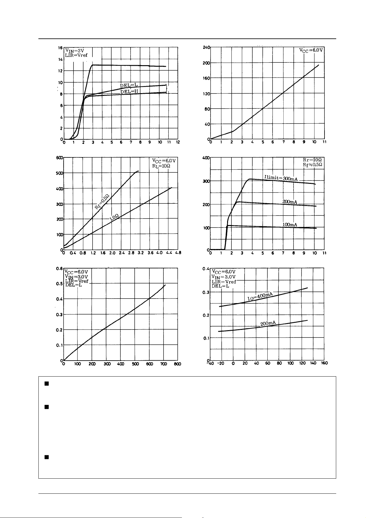
ICC–V
CC
LB1843V
I
IN–VIN
Rf= 0.5 Ω, no load
–mA
CC
Current drain, I
–mA
limit
Set output current, I
Brake
Supply voltage, VCC–V
I
limit–VLIR
Bidirectional
–µA
IN
Input current, I
–mA
limit
Set output current, I
Input voltage, VIN–V
I
limit–VCC
V
–V
LIR
VO(sat) – I
(sat) – V
O
Output saturation voltage, V
O
(sat) – V
O
Output saturation voltage, V
Output current, IO–mA
Supply voltage, VCC–V
(sat) – Ta
V
O
Ambient temperature, Ta – °C
No products described or contained herein are intended for use in surgical implants, life-support systems,
aerospace equipment, nuclear power control systems, vehicles, disaster/crime-prevention equipment and the like,
the failure of which may directly or indirectly cause injury, death or property loss.
Anyone purchasing any products described or contained herein for an above-mentioned use shall:
1 Accept full responsibility and indemnifyanddefend SANYO ELECTRIC CO., LTD., its affiliates, subsidiaries and
distributors and all their officers and employees, jointly and severally, against any and all claims and litigation
and all damages, cost and expenses associated with such use:
2 Not impose any responsibility for any fault or negligence which may be cited in any such claim or litigation on
SANYO ELECTRIC CO., LTD., its affiliates, subsidiaries and distributors or any of their officers and employees
jointly or severally.
Information (including circuit diagrams and circuit parameters) herein is for example only; it is not guaranteed for
volume production. SANYO believes information herein is accurate and reliable, but no guarantees are made or
implied regarding its use or any infringements of intellectual property rights or other rights of third parties.
This catalog provides information as of October, 1996. Specifications and information herein are subject to change without notice.
No.4385-6/6
 Loading...