

Page 1
Ordering number : EN6199A
LB1877M
Monolithic Digital IC
LB1877M
Brushless Motor Driver with Speed Control
for Portable Cassette Recorders
Overview
The LB1877M is a motor driver well suited for driving
motors of minicassette recorders, headphone stereos, and
microcasette recorders that use a 3V power supply.
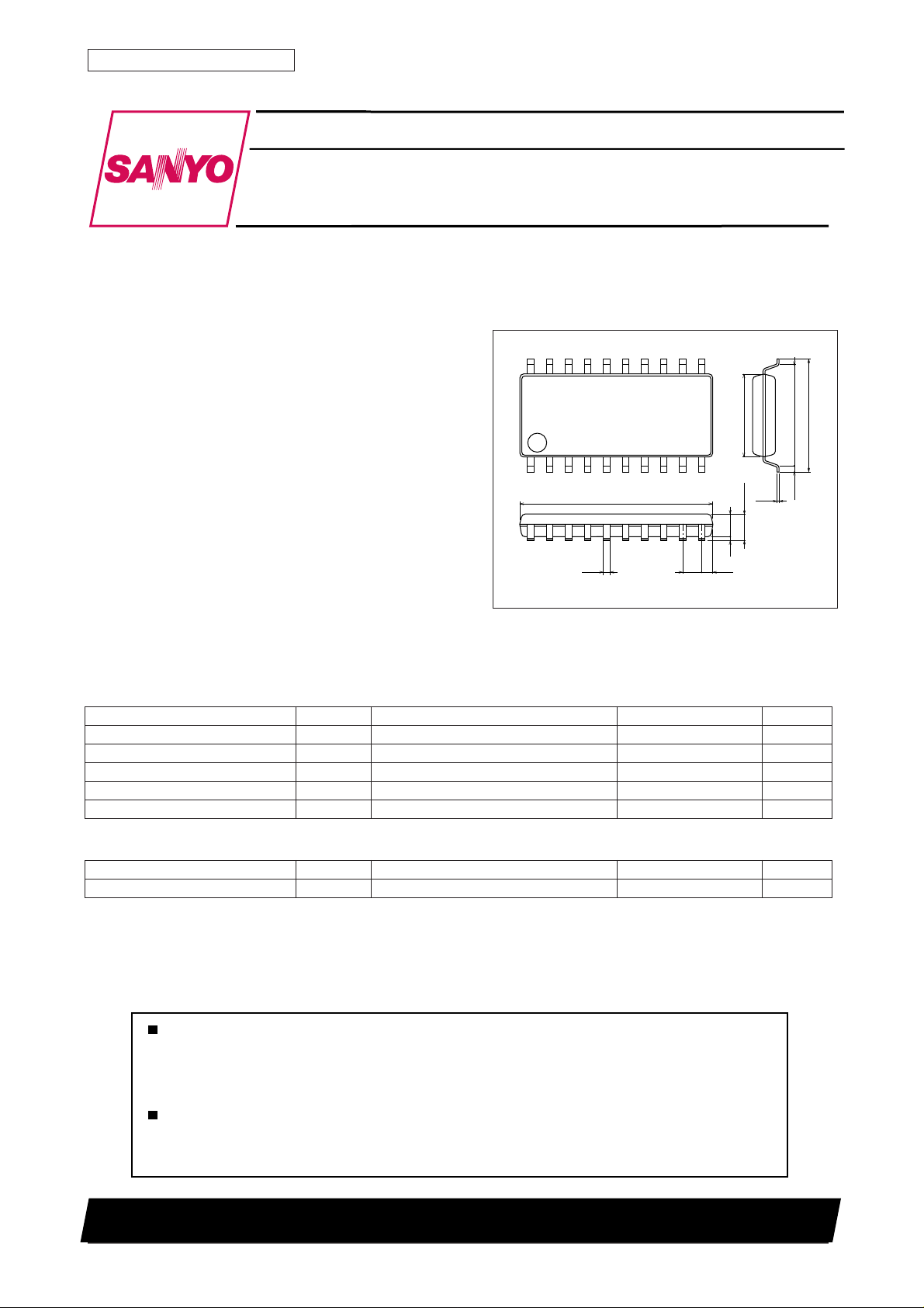
Package Dimensions
unit: mm
3036B-MFP20
20
[LB1877M]
11
5.4
Functions and Features
• Brushless sensorless motor drive (3-phase half-wave drive)
• Forward/reverse drive possible
• Built-in speed control function (voltage servo)
• Built-in reference voltage (0.9V)
• Soft switching
1
12.6
0.35
10
1.27
0.15
1.8 max
1.50.1
0.59
SANYO : MFP20
Specifications
Absolute Maximum Ratings at Ta = 25°C
Parameter Symbol Conditions Ratings Unit
Maximum supply voltage V
Maximum output current IO max 0.5 A
Allowable power dissipation Pd max 0.5 W
Operating temperature Topr –10 to +80 °C
Storage temperature Tstg –40 to +150 °C
max 6.0 V
CC
6.35
0.625
7.6
Allowable Operating Ranges at Ta = 25°C
Parameter Symbol Conditions Ratings Unit
Power supply voltage V
Any and all SANYO products described or contained herein do not have specifications that can handle
applications that require extremely high levels of reliability, such as life-support systems, aircraft's
control systems, or other applications whose failure can be reasonably expected to result in serious
physical and/or material damage. Consult with your SANYO representative nearest you before using
any SANYO products described or contained herein in such applications.
SANYO assumes no responsibility for equipment failures that result from using products at values that
exceed, even momentarily, rated values (such as maximum ratings, operating condition ranges, or other
parameters) listed in products specifications of any and all SANYO products described or contained
herein.
CC
SANYO Electric Co.,Ltd. Semiconductor Company
TOKYO OFFICE Tokyo Bldg., 1-10, 1 Chome, Ueno, Taito-ku, TOKYO, 110-8534 JAPAN
1.8 to 5.0 V
63099RM(KI)
No. 6199-1/7
Page 2
LB1877M
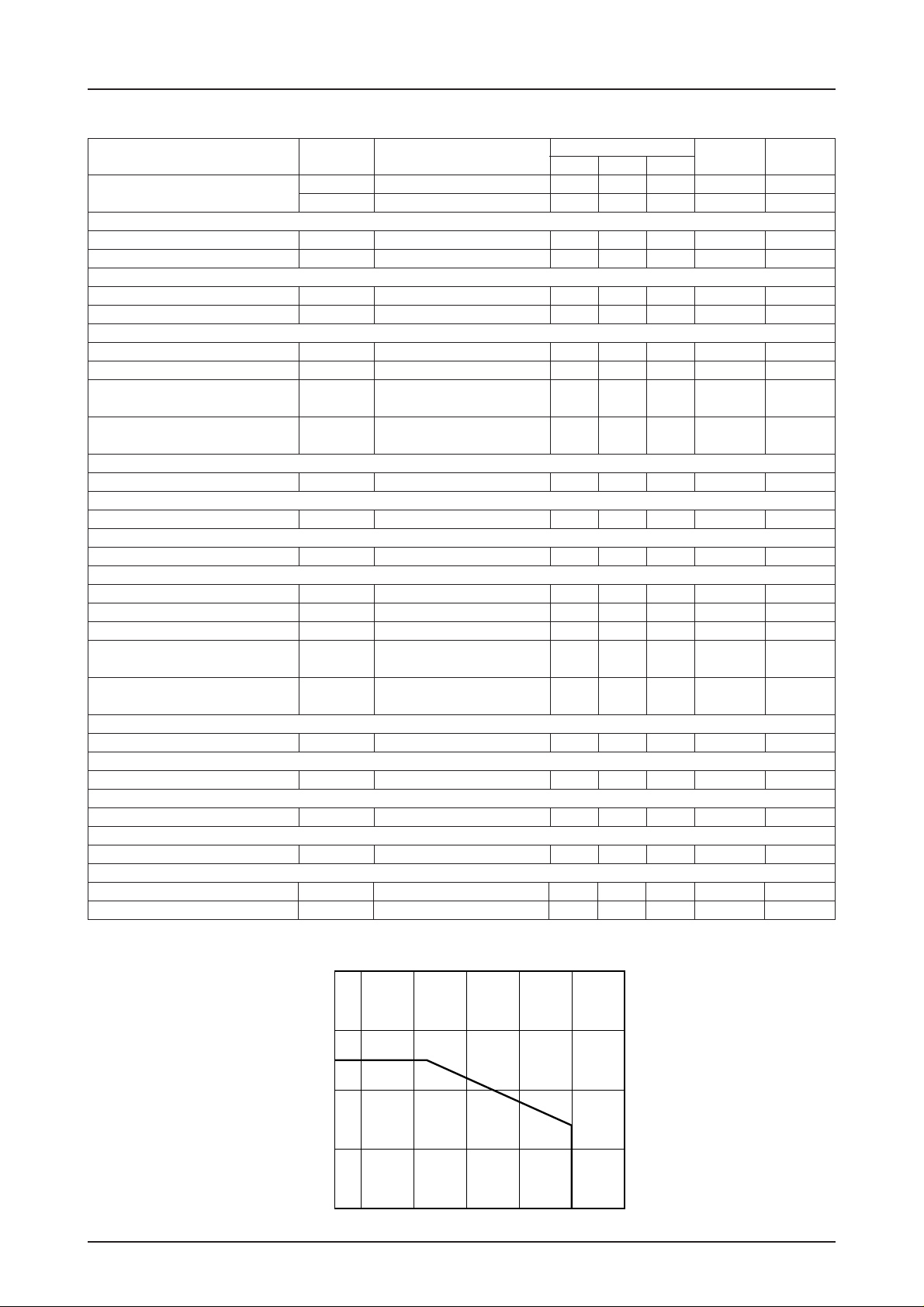
Electrical Characteristics at Ta = 25°C, VCC = 2.4V
Parameter Symbol Conditions
Ratings
min typ max circuit
Unit
Power supply current ICC1 S/S pin High level 4.0 mA 1
ICC2 S/S pin Low level (standby) 20 µA2
[S/S pin]
S/S pin High level SSH Start 1.5 V
CC
S/S pin Low level SSL Stop 0 0.3 V 4
[DR pin]
DR pin High level DRH Reverse 1.5 V
CC
DR pin Low level DRL Normal direction 0 0.3 V 10
[Internal reference voltage]
Internal reference voltage VREF Output current 0 µA 0.8 0.9 1.0 V 11
Output current IREF Output current 250 µA 25 mV/250 µA12
Reference voltage to power supply
∆VREF/∆VCCV
= 1.8 to 5.0V 5 mV/V 13
CC
voltage characteristics
Reference voltage to temperature ∆IREF/∆Ta VCC = 2.4V – 0.1 0.3 mV/°C Target
characteristics
[OSC pin]
Charge current Isc 3.0 4.5 6.0 µA14
[COM pin]
Sink current ICOM 17 24 33 µA15
[LB pin]
Charge current ILB 4.5 6.5 9.0 µA16
[VSP pin]
Input voltage range VIN VCC = 2.4V 0.15 1.8 V 17
Speed signal detection precision VSP VIN = 1V 420 500 580 mV 18
Speed signal relative precision RSP – 6 6 % Target
Speed signal to power supply
∆VSP/∆VCCVCC = 1.8 to 5.0V 2.5 mV/V 19
voltage characteristics
Speed signal to temperature ∆VSP/∆Ta – 0.1 0.2 mV/°C Target
characteristics
[IN+ pin]
Input voltage range VIN+ VCC = 2.4V 0.1
VCC – 0.7
[OUT pin]
Output current IOUT VIN+ = 1V 25 30 47.3 µA21
[RI pin]
Current detection precision VRI RI = 10 kΩ U, V, Wout = 2.3V 10 20 35 mV 22
[U, V, WOUT pins]
Output saturation voltage Vsat IO = 200 mA 0.25 V 23
[Thermal]
Thermal protection trigger temperature
TTSD 180 °C Target
Temperature hysteresis width ∆TTSD 15 °C Target
Note: Items shown to be Target are not measured.
Measurement
V3
V9
V20
0.8
0.6
0.5
0.4
0.2
Pd max – Ta
Allowable power dissipation, Pd max – W
0
0 20406080100–10
Ambient temperature, Ta – °C
No. 6199-2/7
Page 3
LB1877M
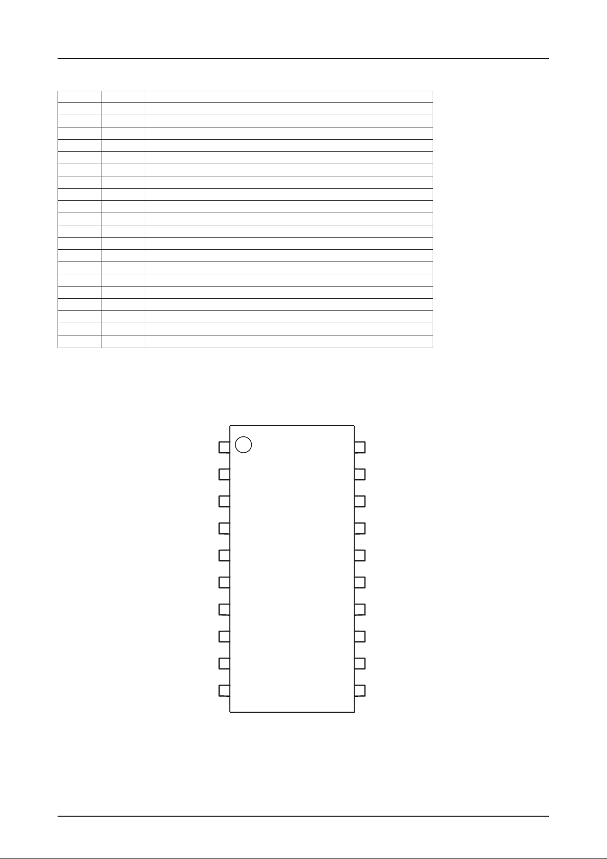
Pin Function
Pin number Pin name Function
20 UOUT U-phase output
1 VOUT V-phase output
2 WOUT W-phase output
6 UB U-phase base of 3-phase differential
5 VB V-phase base of 3-phase differential
4 WB W-phase base of 3-phase differential
18 VCC Power supply
7 OSC Startup oscillator pin
8 COM Output waveform detection comparator voltage
3 P – GND Output transistor and predriver ground
9 GND Ground pin
11 S/S Start/stop pin
19 DR Forward/reverse pin
12 VREF Reference voltage 0.9V
14 VSP Output waveform peak detection pin
13 IN+ Error amp non-inverted pin
15 OUT Error amp output pin
10 RI Current feedback resistor connection pin
16 FC Frequency response adjustment pin
17 LB Motor start lockup prevention. Connect to GND via capacitor
Pin Assignment
VOUT
WOUT
PGND
WB
VB
UB
OSC
1
2
3
4
5
20
UOUT
19
DR
18
VCC
17
LB
16
FC
LB1877M
6
7
8
COM
9
GND
10
RI
15
OUT
14
VSP
13
IN+
12
VREF
11
S/S
Top view
No. 6199-3/7
Page 4
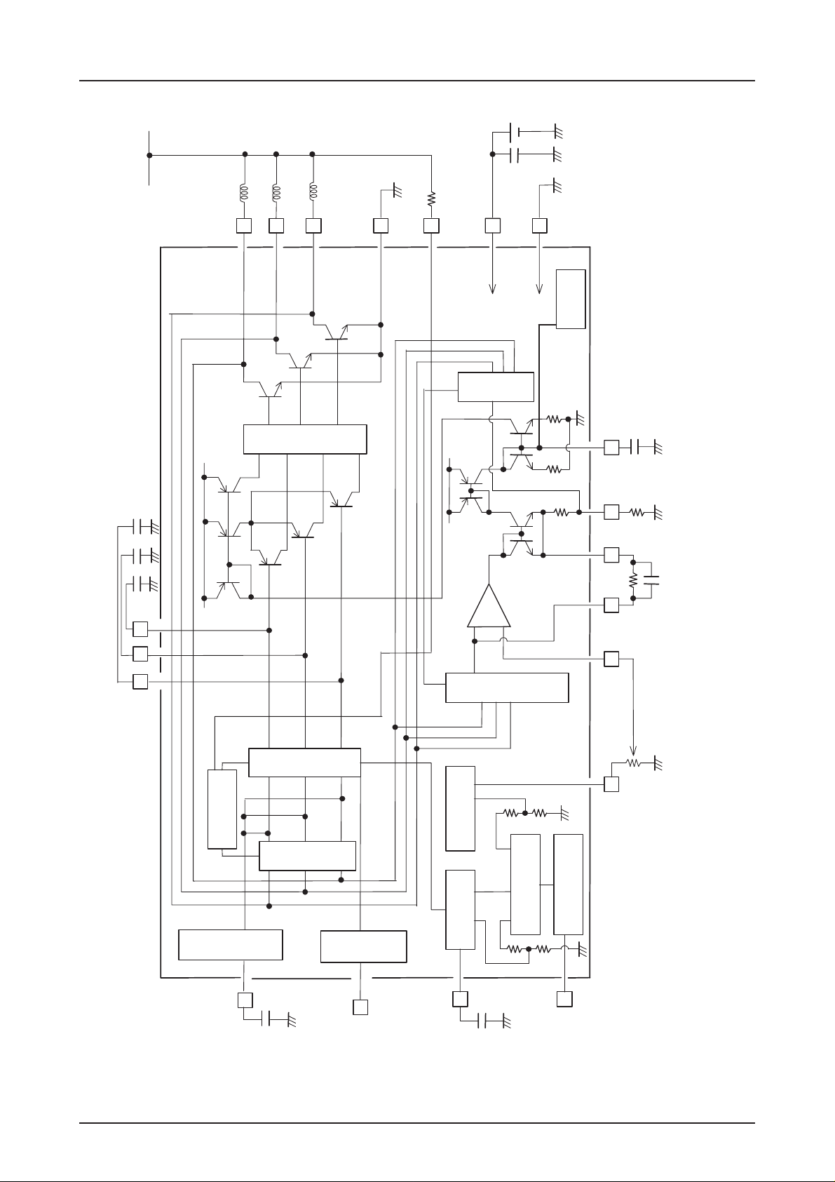
Block Diagram
–
+
WBVB
UB
V
CC
UOUT
VOUT
WOUT
GND
3V
COM
V
CC
FCRIOUTVspIN+VREF
S/S
DR
LB
0.047µF
OSC
P–GND
TSD
0.22µF
0.47µF
0.1µF
1kΩ
100kΩ
10kΩ
0.1µF0.1µF
0.1µF
Predriver
Lockup
prevention
Waveform
detection
Transfer current
start logic
Forward/
reverse
Startup
detection
Oscillator
Speed control
reference voltage
Reference
voltage
Power supply
bias
* Constants given in the illustration are for reference only and are not guaranteed for all motors.
Individual adjustment for each motor is required.
Speed detection
Current
detection
To various blocks
To control block
LB1877M
No. 6199-4/7
Page 5
LB1877M
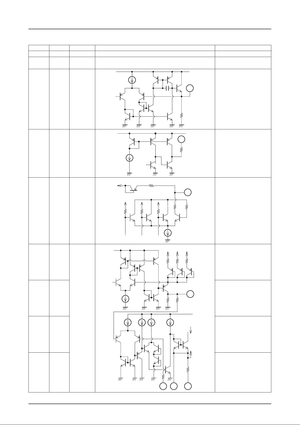
Pin Description Unit (resistance: Ω, capacitance: F)
Pin number
18
9
12
Pin name
VCC
GND
VREF
Pin voltage
1.8V to 5.0V
0.7V to 0.9V
Equivalent circuit
50k
12
Pin function
Power supply for all circuits
Ground for all circuits except
FC and power block.
Internal reference voltage.
Connected as speed control
voltage to IN+ pin via external
resistor.
14
7
8
OSC
COM
VSP
1V to Vcc
1.3V to Vcc
0.1V to
Vcc – 0.7V
To comparator input
To UOUT
20k
20k
10k
To WOUTTo VOUT
20k
7
200
1k 20k
To U,V,WOUT
10k 10k 10k
Startup oscillator pin.
Adjusts self-excitation
frequency via external
capacitor.
Determines threshold voltage
of waveform detection circuit.
8
Connected to Vcc via an
external resistor.
Varies the startup threshold
voltage.
Peak detection circuit output
pin.
13
15
10
IN+
OUT
RI
200
14
2005k
Drive
current
I
Current feedback circuit
10k
101513
Error amplifier non-inverted
pin.
Controls rotation speed via
input pin voltage.
Error amplifier output pin.
Connect external resistor
between Vsp pins for
feedback.
Current feedback output pin.
Connect external resistor
between this pin and ground
for current feedback
adjustment.
Continued on next page
No. 6199-5/7
Page 6
LB1877M
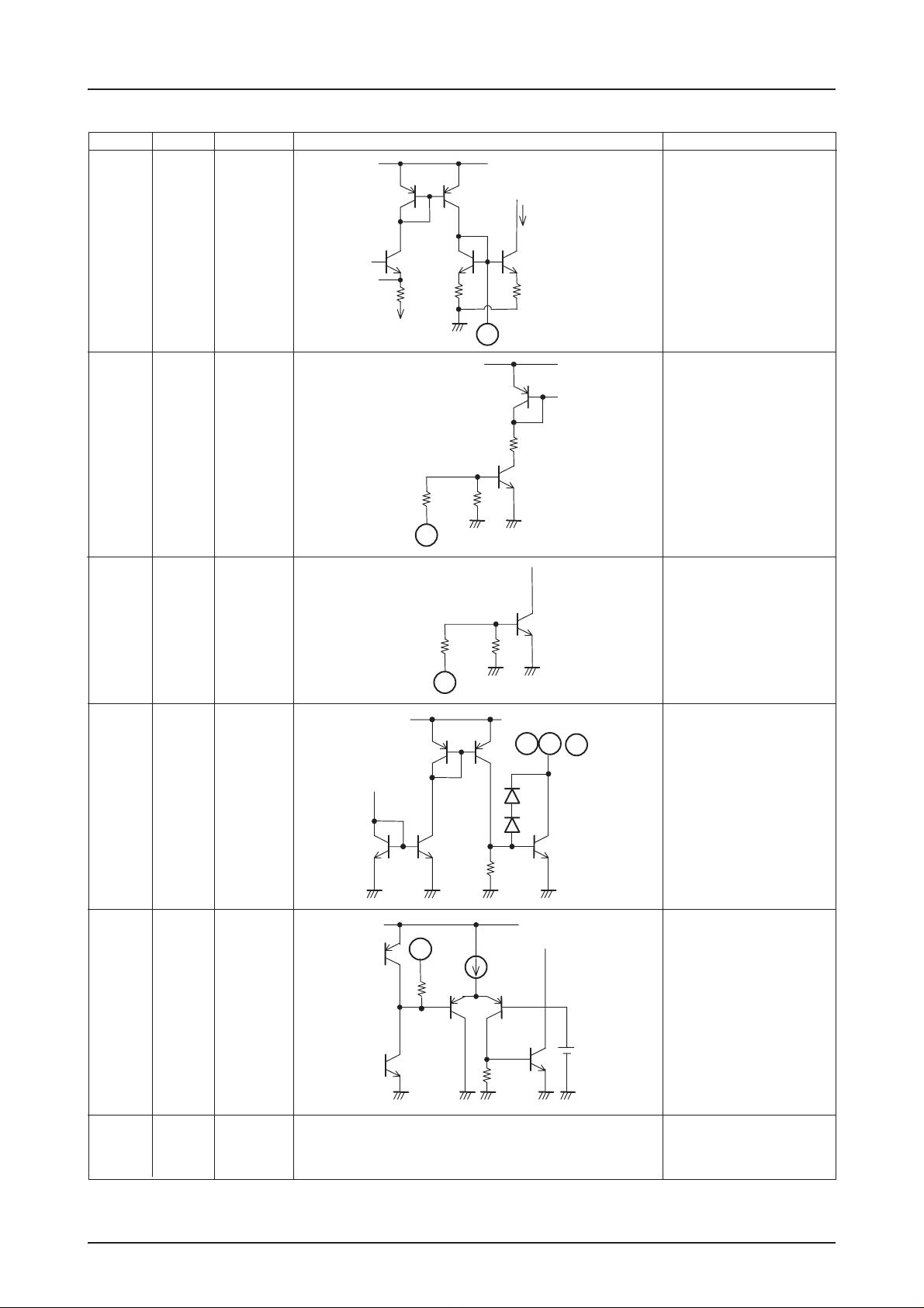
Continued from preceding page Unit (resistance: Ω, capacitance: F)
Pin number
16
Pin name
FC
Pin voltage
Voltage
input not
allowed
Equivalent circuit
6k
3S
Drive current
2k
Pin function
Frequency characteristics
adjustment pin.
Connect to ground via
capacitor.
11
19
20
S/S
To RI pin
0 to Vcc
16
Start/stop pin.
80k
50k50k
11
DR
0 to Vcc
Forward/reverse rotation pin.
50k50k
19
UOUT
1
VOUT
0 to 8V
20 1
U, V, W phase output pins.
2
Connect to motor coils
17
2
WOUT
LB
0 to 1V
100k
Motor start lockup prevention.
17
200
3
P – GND
Power block ground.
Continued on next page
No. 6199-6/7
Page 7
Continued from preceding page
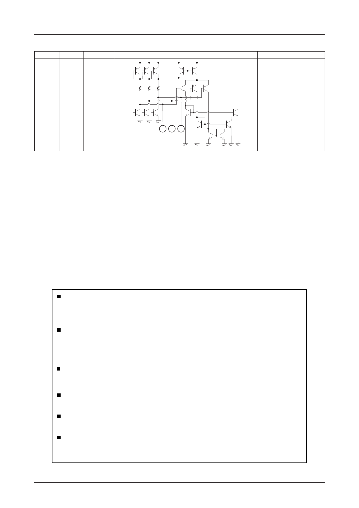
Pin number
4
5
6
Pin name
WB
VB
UB
Pin voltage
Voltage
input not
allowed
LB1877M
Equivalent circuit
4 5 6
Pin function
Base pins for U, V, W
differential.
Connect to ground via
capacitor for soft switching
Specifications of any and all SANYO products described or contained herein stipulate the performance,
characteristics, and functions of the described products in the independent state, and are not guarantees
of the performance, characteristics, and functions of the described products as mounted in the customer's
products or equipment. To verify symptoms and states that cannot be evaluated in an independent device,
the customer should always evaluate and test devices mounted in the customer's products or equipment.
SANYO Electric Co., Ltd. strives to supply high-quality high-reliability products. However, any and all
semiconductor products fail with some probability. It is possible that these probabilistic failures could
give rise to accidents or events that could endanger human lives, that could give rise to smoke or fire,
or that could cause damage to other property. When designing equipment, adopt safety measures so
that these kinds of accidents or events cannot occur. Such measures include but are not limited to protective
circuits and error prevention circuits for safe design, redundant design, and structural design.
In the event that any or all SANYO products(including technical data,services) described or
contained herein are controlled under any of applicable local export control laws and regulations,
such products must not be exported without obtaining the export license from the authorities
concerned in accordance with the above law.
No part of this publication may be reproduced or transmitted in any form or by any means, electronic or
mechanical, including photocopying and recording, or any information storage or retrieval system,
or otherwise, without the prior written permission of SANYO Electric Co. , Ltd.
Any and all information described or contained herein are subject to change without notice due to
product/technology improvement, etc. When designing equipment, refer to the "Delivery Specification"
for the SANYO product that you intend to use.
Information (including circuit diagrams and circuit parameters) herein is for example only ; it is not
guaranteed for volume production. SANYO believes information herein is accurate and reliable, but
no guarantees are made or implied regarding its use or any infringements of intellectual property rights
or other rights of third parties.
This catalog provides information as of June, 1999. Specifications and information herein are subject to change
without notice.
PS
No. 6199-7/7
 Loading...