

Page 1
Overview
The LB1872 is a 3-phase brushless motor driver IC
developed for driving the polygon mirror motor used in
laser printers and similar products.
Functions and Features
• Integrates the circuits (speed control and driver circuits)
required for laser printer polygon mirror motor drive in a
single chip.
• Uses a current linear drive technique for minimal motor
noise. Only a small capacitors are required for output
oscillation prevention.
• PLL speed control adopted for high-precision rotation
with excellent jitter characteristics.
• Phase lock detection output with a chattering prevention
function
• Four rotation rates can be set up using a single crystal
oscillator to support 240, 300, 400, and 600 dpi
operation.
• Arbitrary rotation rates can be acquired when an
external clock is used.
• Deceleration function implemented by short-circuit
braking (free running when stopped)
• Built-in FG and error amplifiers
• Full complement of protection circuits, including
thermal protection, low voltage protection, and current
limiter circuits, provided on chip.
Package Dimensions
unit: mm
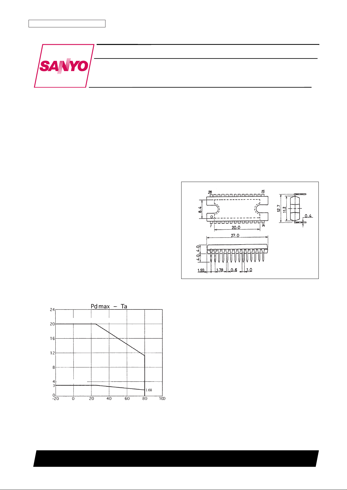
3147B-DIP28H
Monolithic Digital IC
13098HA(OT) No. 5625-1/11
SANYO: DIP28H
[LB1872]
SANYO Electric Co.,Ltd. Semiconductor Bussiness Headquarters
TOKYO OFFICE Tokyo Bldg., 1-10, 1 Chome, Ueno, Taito-ku, TOKYO, 110-0005 JAPAN
Polygon Mirror Scanner Driver IC
LB1872
Ordering number : EN5625A
Independent IC
Ambient temperature, Ta - °C
Allowable power dissipation, Pd max - W
With an arbitrarily large heat sink
Page 2
No. 5625-2/11
LB1872
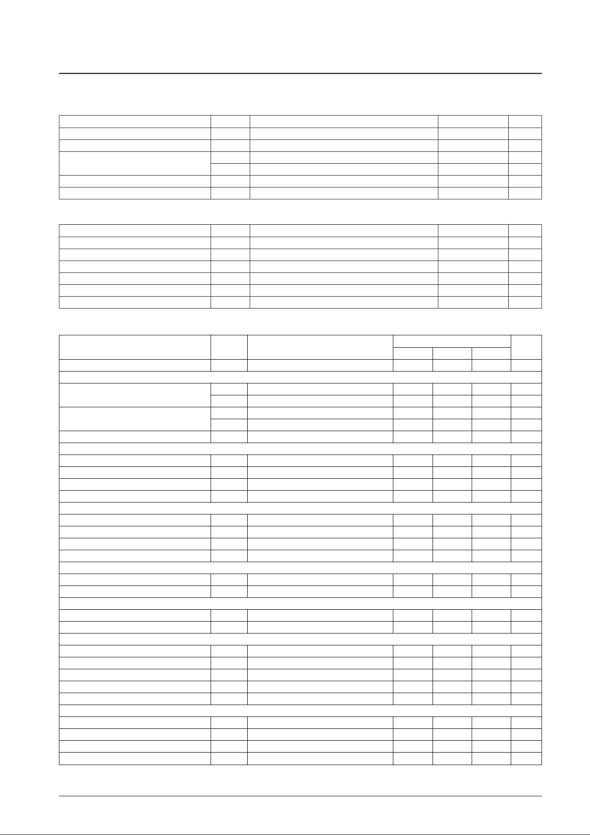
Parameter Symbol Conditions
Ratings
Unit
min typ max
Current drain I
CC
In stop mode 20 27 mA
[Output Saturation Voltage] V
AGC
= 2 V
Source
V(sat)1-1 I
O
= 0.7 A, RF= 0 Ω 1.5 1.9 V
V(sat)1-2 I
O
= 1.5 A, RF= 0 Ω 1.8 2.2 V
Sink
V(sat)2-1 I
O
= 0.7 A, RF= 0 Ω 0.3 0.5 V
V(sat)2-2 I
O
= 1.5 A, RF= 0 Ω 0.7 1.0 V
Output leakage current I
O
(leak) VCC= 28 V 100 µA
[5-V Fixed-Voltage Output]
Output voltage V
REG
4.65 5.0 5.35 V
Voltage regulation ∆V
REG
1 VCC= 10 to 28 V 40 100 mV
Load regulation ∆V
REG
2 IO= 0 to 10 mA 20 100 mV
Temperature coefficient ∆V
REG
3 Design target value 0 mV/°C
[Hall Input Block]
Input bias current I
B(HA)VAGC
= 3 V 2 10 µA
Differential-mode input range V
HIN
With a sine wave input 50 350 mV
Common-mode input range V
ICM
Differential input: 50 mV p-p 3.5 VCC– 3.5 V
Input offset voltage V
IOH
Design target value –20 +20 mV
[Low Voltage Protection Circuit]
Operating voltage V
SD
8.4 8.8 9.2 V
Hysteresis ∆V
SD
0.2 0.4 0.6 V
[Thermal Protection Circuit]
Shutdown temperature TSD Design target value (junction temperature) 150 180 °C
Hysteresis ∆TSD Design target value (junction temperature) 40 °C
[FG Amplifier]
Input offset voltage V
IO(FG)
Design target value –10 +10 mV
Input bias current I
B(FG)
–1 +1 µA
DC bias level V
B(FG)
–5% 1/2V
REG
+5% V
Output high-level voltage V
OH(FG)IOH
= –500 µA V
REG
– 1.2 V
REG
– 0.8 V
Output low-level voltage V
OL(FG)IOL
= 500 µA 0.8 1.2 V
[FG Schmitt Input Block]
Input hysteresis (high to low) V
SHL
0 mV
Input hysteresis (low to high) V
SLH
150 mV
Hysteresis V
FGL
100 150 200 mV
Input operating level V
FGSIL
400 mV
Electrical Characteristics at Ta = 25°C, VCC= 24 V
Parameter Symbol Conditions Ratings Unit
Supply voltage V
CC
10 to 28 V
5.0-V fixed-voltage output current I
REG
0 to –15 mA
LD pin voltage V
LD
0 to 28 V
FGS pin voltage V
FGS
0 to 28 V
LD pin output current I
LD
0 to 10 mA
FGS pin output current I
FGS
0 to 5 mA
Allowable Operating Ranges at Ta = 25°C
Parameter Symbol Conditions Ratings Unit
Maximum supply voltage V
CC
max 30 V
Maximum output current I
O
max t ≤0.5s 2.0 A
Allowable power dissipation
Pd max1 Independent IC 3 W
Pd max2 Arbitrarily large heat sink 20 W
Operating temperature Topr –20 to +80 °C
Storage temperature Tstg –55 to +150 °C
Specifications
Absolute Maximum Ratings at Ta = 25°C
Continued on next page.
Page 3
No. 5625-3/11
LB1872
Continued from preceding page.
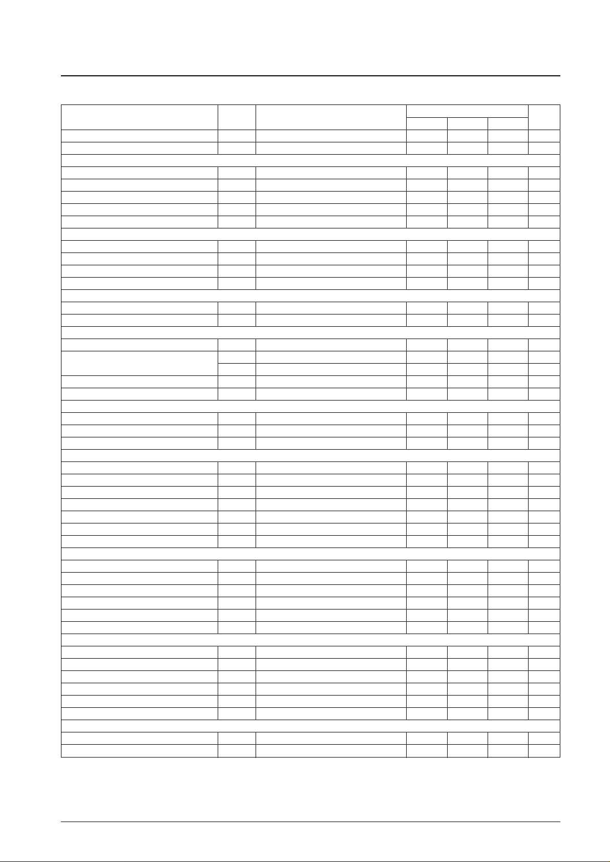
Parameter Symbol Conditions
Ratings
Unit
min typ max
Output saturation voltage V
FGS(sat)IFGS
= 3 mA 0.2 0.4 V
Output leakage current I
L(FGS)VCC
= 28 V 10 µA
[Error Amplifier]
Input offset voltage V
IO(ER)
Design target value –10 +10 mV
Input bias current I
B(ER)
–1 +1 µA
DC bias level V
B(ER)
–5% 1/2V
REG
+5% V
Output high-level voltage V
OH(ER)IOH
= –500 µA V
REG
– 1.2 V
REG
– 0.8 V
Output low-level voltage V
OL(ER)IERI
= 100 µA, IOL= 500 µA 0.7 1.0 1.3 V
[Phase Comparator Output]
Output high-level voltage V
PDHIOH
= –100 µA V
REG
– 0.2 V
REG
– 0.1 V
Output low-level voltage V
PDLIOL
= 100 µA 0.1 0.2 V
Output source current I
PD
+ VPD= V
REG
/2 –0.6 mA
Output sink current I
PD
– VPD= V
REG
/2 1.5 mA
[Lock Detection Output]
Output saturation voltage V
LD(sat)ILD
= 5 mA 0.1 0.4 V
Output leakage current I
LDLEAKVCC
= 28 V 10 µA
[Drive Block]
Output idling voltage V
ID
6 mV
Forward gain
G
DF
1 When the phase is locked 0.4 0.5 0.6
G
DF
2 When unlocked 2.4 3.0 3.6
Current limiter V
L
Rf = 2 Ω 0.45 0.5 0.55 V
Brake command voltage V
BRK
2.3 V
[Reference Signal Block]
Crystal oscillator frequency f
OSC
In crystal oscillator mode 1 10 MHz
Low-level pin voltage V
OSCLIOSC
= –0.5 mA 1.7 V
High-level pin voltage I
OSCHVOSC
= V
OSCL
+ 0.3 V 0.5 mA
[N1 Pin]
External input frequency f
I
(N1) In external clock mode 100 10000 Hz
High-level input voltage V
IH
(N1) 3.5 V
REG
V
Low-level input voltage V
IL
(N1) 0 1.5 V
Input open voltage V
IO
(NI) V
REG
– 0.5 V
REG
V
Hysteresis V
IS
(N1) 0.3 0.4 0.5 V
High-level input current I
IH
(N1) VN1 = V
REG
–10 0 +10 µA
Low-level input current I
IL
(N1) VN1 = 0 V –350 –275 µA
[N2 Pin]
High-level input voltage V
IH
(N2) 4.0 V
REG
V
Middle-level input voltage V
IM
(N2) 2.0 3.0 V
Low-level input voltage V
IL
(N2) 0 1.0 V
Input open voltage V
IO
(N2) 2.2 2.5 2.8 V
High-level input current I
IH
(N2) VN2 = V
REG
200 270 µA
Low-level input current I
IL
(N2) VN2 = 0 V –270 –200 µA
[S/S Pin]
High-level input voltage V
IH
(SS) 3.5 V
REG
V
Low-level input voltage V
IL
(SS) 0 1.5 V
Input open voltage V
IO
(SS) V
REG
– 0.5 V
REG
V
Hysteresis V
IS
(SS) 0.3 0.4 0.5 V
High-level input current I
IH
(SS) VS/S = V
REG
–10 0 +10 µA
Low-level input current I
IL
(SS) VS/S = 0 V –350 –275 µA
[CLD Pin]
Charge current I
CLD
1 V
CLD
= 0 V (Phase locked) –9 –7 –5 µA
Discharge current I
CLD
2 VCL= V
REG
/2 (Phase unlocked) 1 mA
Page 4
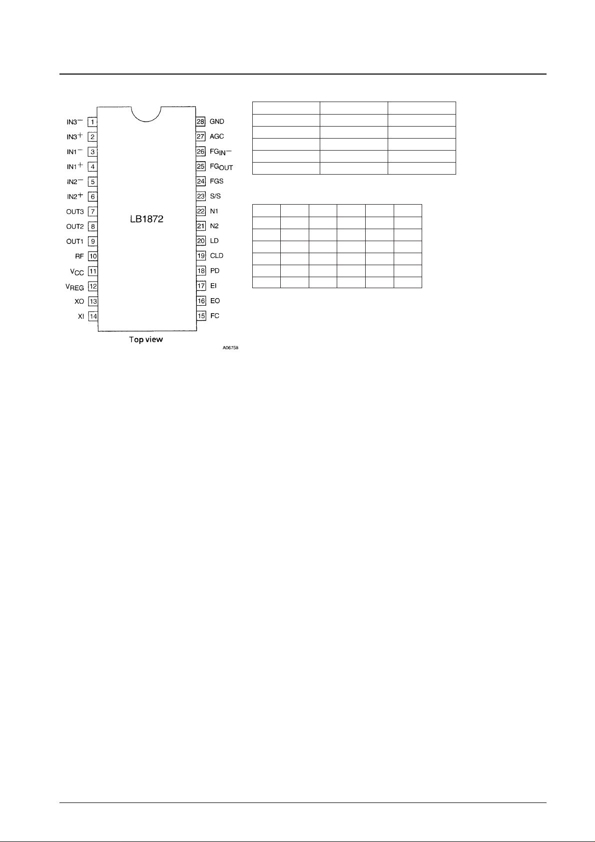
Pin Assignment
No. 5625-4/11
LB1872
Clock Divisor Switching
N1 N2 Divisor
H H 2048 (4
× 1 × 512)
H L 4096 (4 × 2 × 512)
L H 5120 (5 × 2 × 512)
L L 3072 (3 × 2 × 512)
CLK IN M or open EXT. CLK
Three-Phase Logic Truth Table
H1 H2 H3 OUT1 OUT2 OUT3
H L H L H M
H L L L M H
H H L M L H
L H L H L M
L H H H M L
L L H M H L
Page 5
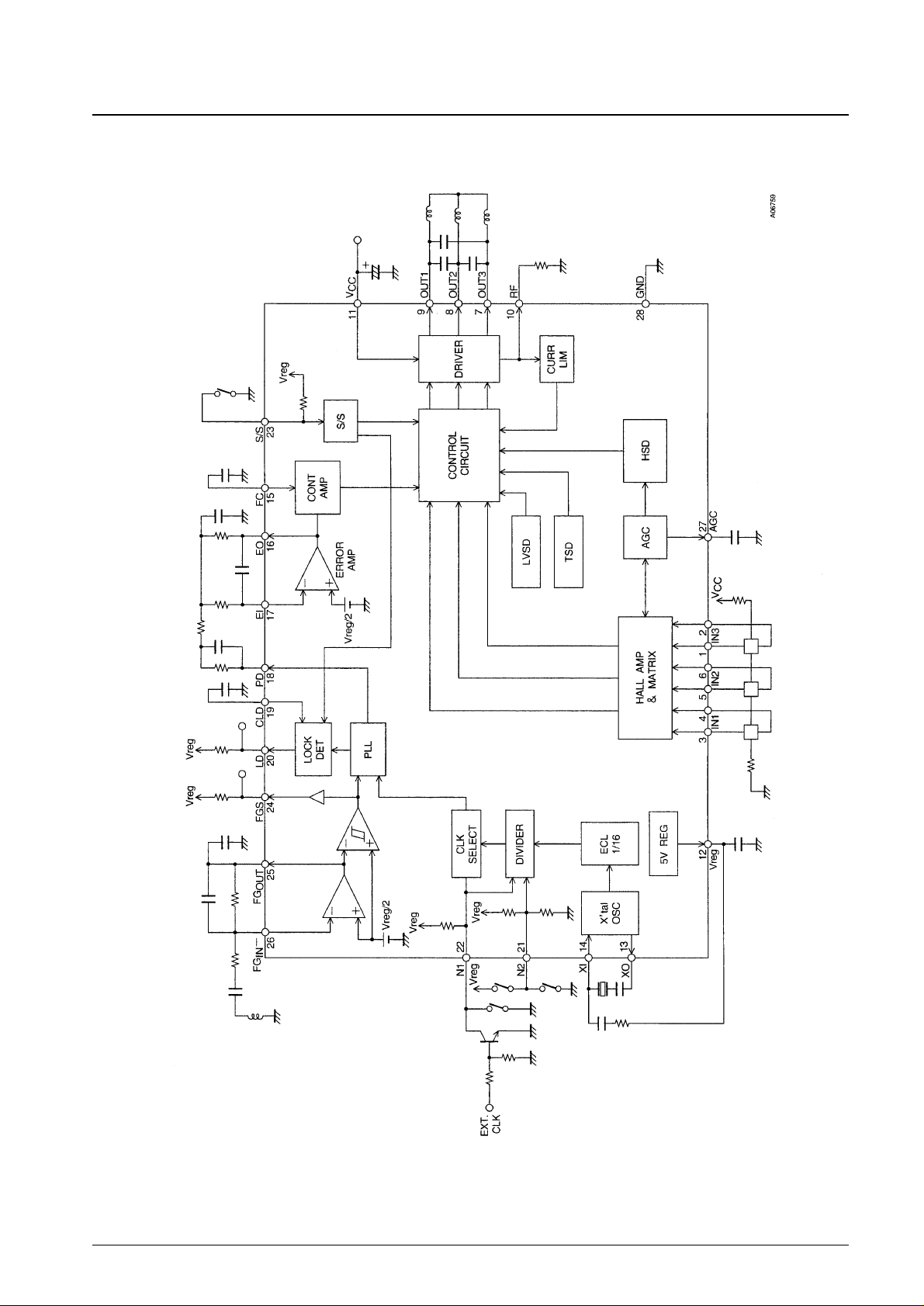
Equivalent Circuit Block Diagram
No. 5625-5/11
LB1872
Page 6
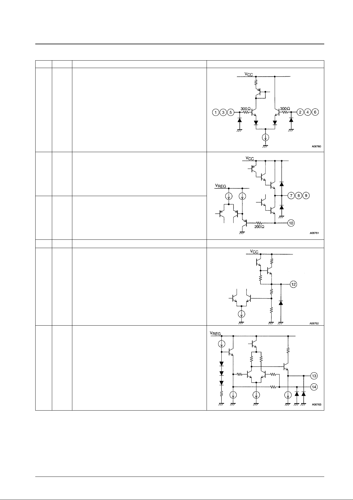
Pin No. Symbol Pin function Equivalent circuit
No. 5625-6/11
LB1872
Pin Functions
1
2
3
4
5
6
IN3
–
IN3
+
IN1
–
IN1
+
IN2
–
IN2
+
Hall amplifier inputs
IN
+
> IN–is the input high state, and the reverse is the input low state.
Connect a capacitor between the IN
+
and IN–inputs if there is noise in
the Hall sensor signals.
An amplitude of over 50 mV p-p and under 350 mV p-p is desirable in
the Hall sensor signals. Kickback may occur in the output if the input
signal has an amplitude greater than 350 mV p-p.
7
8
9
OUT3
OUT2
OUT1
Motor drive outputs
Connect capacitors between the motor outputs (or between the motor
outputs and ground) if oscillation occurs in the outputs. (Use capacitors
in the range 0.1 µF to 0.47 µF.)
10 RF
Output current detection
Connect a resistor (Rf) between this pin and ground.
The output current is limited to be up to I
OUT
= V
REG
/Rf.
11
V
CC
Power supply
12
V
REG
Stabilized power supply output (5-V output)
Connect a capacitor (about 0.1 µF) between this pin and ground for
stabilization.
13
14
XO
XI
Crystal oscillator connections
These pins are used to drive the reference clock oscillator element.
If an external clock (with a frequency of a few MHz) is used, connect a
resistor (about 13 kΩ) to the XI pin in series and input the clock signal
through that resistor. Leave the XO pin open in this case.
Continued on next page.
Page 7
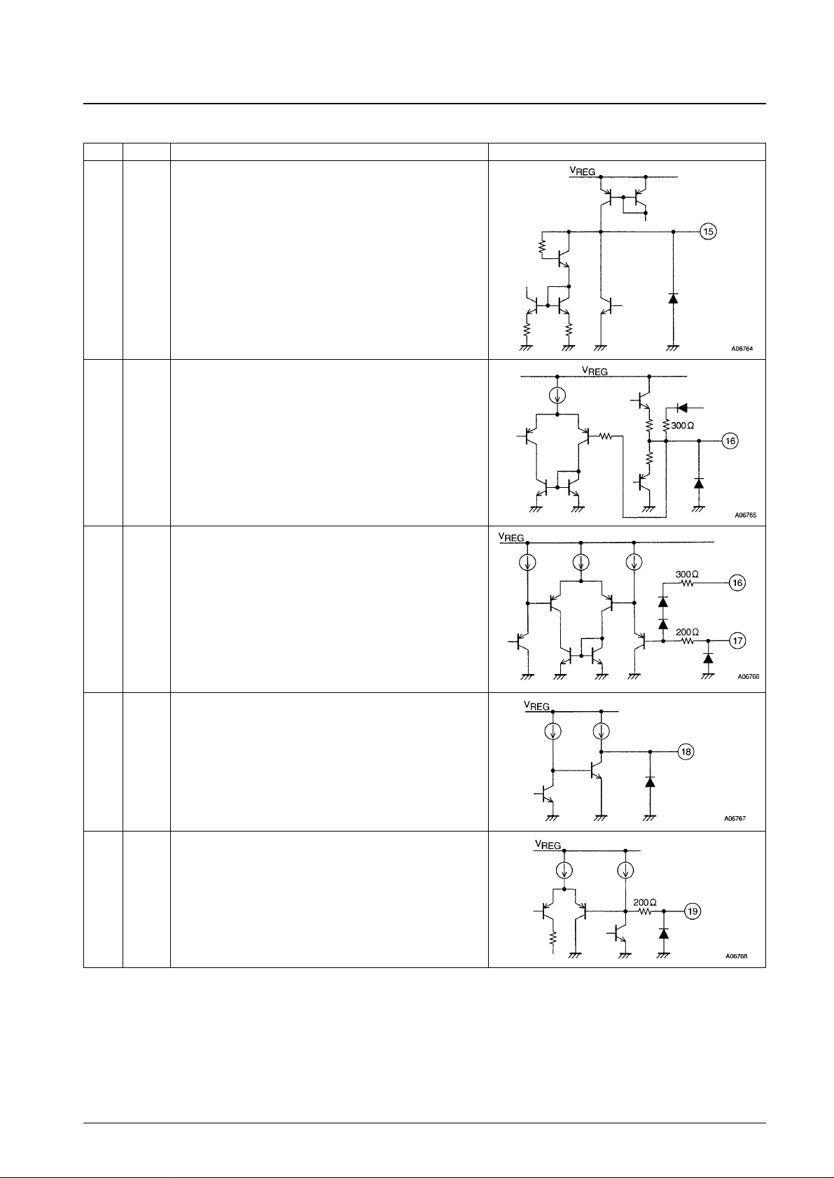
No. 5625-7/11
LB1872
Continued from preceding page.
Pin No. Symbol Pin function Equivalent circuit
15 FC
Control amplifier frequency correction
Current limiter system closed loop oscillation can be prevented by
inserting a capacitor (about 0.022 to 0.47 µF) between this pin and
ground. If the capacitance of this capacitor is too large, the output
current response characteristics may be degraded.
16 EO
Error amplifier output
When high, the output current is increased.
Control
amplifier
17 EI Error amplifier input
18 PD
Phase comparator output (PLL output)
The phase error is output as changes in the duty of a pulse waveform.
The output current is increased as the duty becomes smaller.
19 CLD
LD output mask time setting
Chattering can be masked by inserting a capacitor (about 0.1 to 0.47
µF) between this pin and ground. The startup time may be increased if
only masking is used and the servo constants are not re-optimized.
Continued on next page.
Page 8
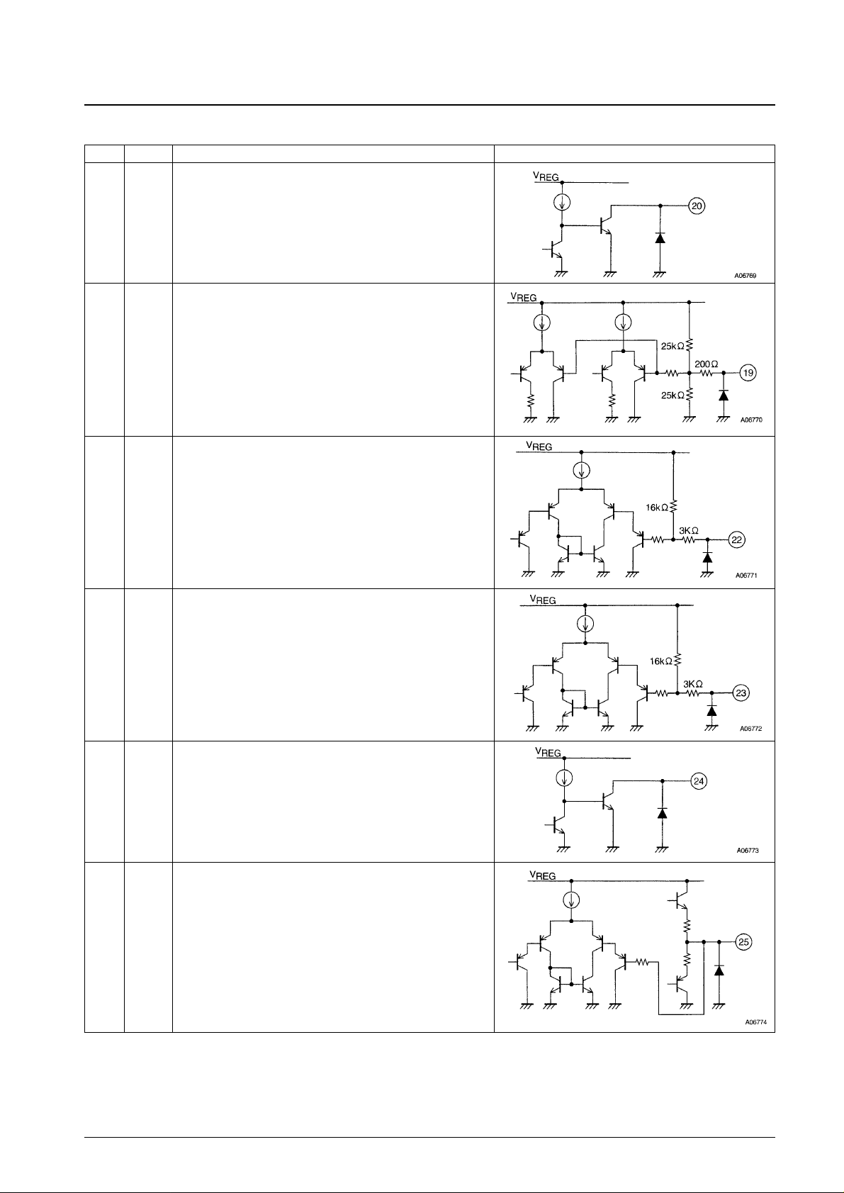
No. 5625-8/11
LB1872
Continued from preceding page.
Pin No. Symbol Pin function Equivalent circuit
20 LD
Phase lock detector output
This pin goes to the on state when the PLL phase is locked. This is an
open collector output.
21 N2
Divisor switch
Low: 0 to 1.0 V
Middle: 2.0 to 3.0 V
High: 4.0 V to V
REG
This pin goes to the middle level when open.
22 N1
Divisor switch and external clock input
Low: 0 to 1.5 V
High: 3.5 V to V
REG
This pin functions as the external clock input pin when N2 is at the
middle level.
This pin goes to the high level when open.
23 S/S
Start/stop control
Low: Start
High: Stop
This pin goes to the high level when open.
24 FGS
FG pulse-converted output
This pin outputs the post-hysteresis comparator FG signal.
This is an open collector output.
25
FG
OUT
FG amplifier output
If noise in the FG signal is a problem, e.g. if discharge noise is
detected, insert a capacitor (about 0.01 to 0.1 µF) between this pin and
ground.
Continued on next page.
FG schmitt comparator
Page 9
No. 5625-9/11
LB1872
Continued from preceding page.
Pin No. Symbol Pin function Equivalent circuit
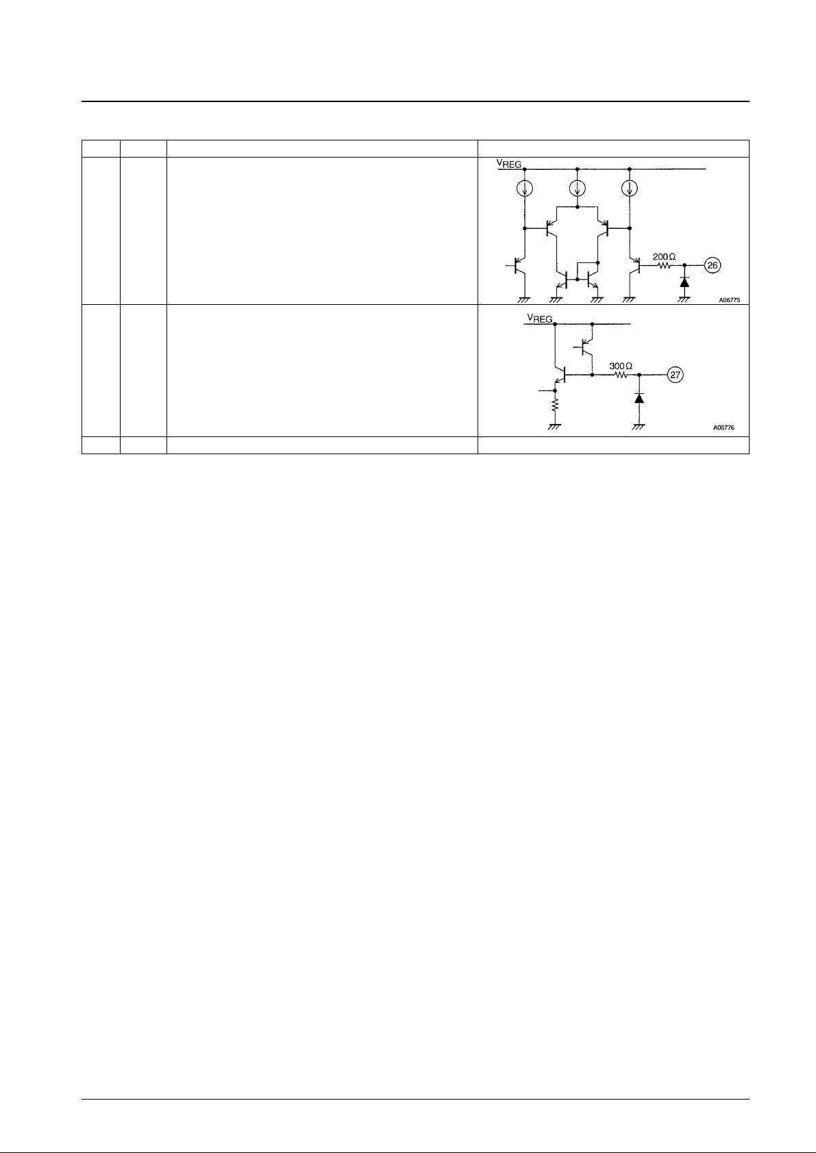
26
FGIN–
FG amplifier input
27 AGC
AGC amplifier frequency characteristics correction
Insert a capacitor (about 0.1 µF) between this pin and ground.
28 GND Ground
LB1872 Functional Description
1. Speed control circuit
Since this IC adopts a PLL speed control circuit, it can provide high-precision, jitter-free, and stable motor operation.
This PLL circuit compares the phases of the CLK (external clock) rising edge and the FG Schmitt output rising edge
and uses the error output from that comparison for control.
If an internal clock system is used, the FG servo frequency is determined by the following formula. Therefore, the
motor speed can be set by setting the number of FG pulses and the crystal oscillator frequency.
fFG(servo) = f
OSC
/N
f
OSC
: Crystal oscillator frequency
N: Clock divisor (See the separately provided table.)
If an external clock (input to the N1 pin) is used, the IC controls the motor speed by holding the FG servo frequency
identical to the external clock frequency.
2. Output drive circuit
To suppress motor noise as much as possible, this IC adopts a three-phase full wave current linear drive technique.
Also, it adopts a midpoint control technique to prevent ASO destruction of the output transistors.
This IC uses short-circuit braking (lower side output) for motor deceleration during speed switching and lock pull in.
In stop mode, the output is turned off.
If a motor with a coil resistance (interphase) of 10 Ω or lower is used, diodes (rectifying) may be inserted between the
outputs and ground (for all outputs) and current limitation may also be applied during braking to prevent excessive
braking currents. Although this is disadvantageous from an ASO standpoint, since states with a large back EMF are
states with a high switching frequency and the amount of time during which loads are applied to the transistors will
be shorter, ASO problems will not be particular severe.
3. Current limiter circuit
The current limiter circuit is a peak current limiter whose limit current is determined by I = VRF/Rf (where VRF = 0.5
V (typical) and Rf is the current detection resistor).
Page 10
4. Reference clock
Any one of the following three techniques can be used to input the reference clock used for speed control.
• Crystal oscillator generated clock
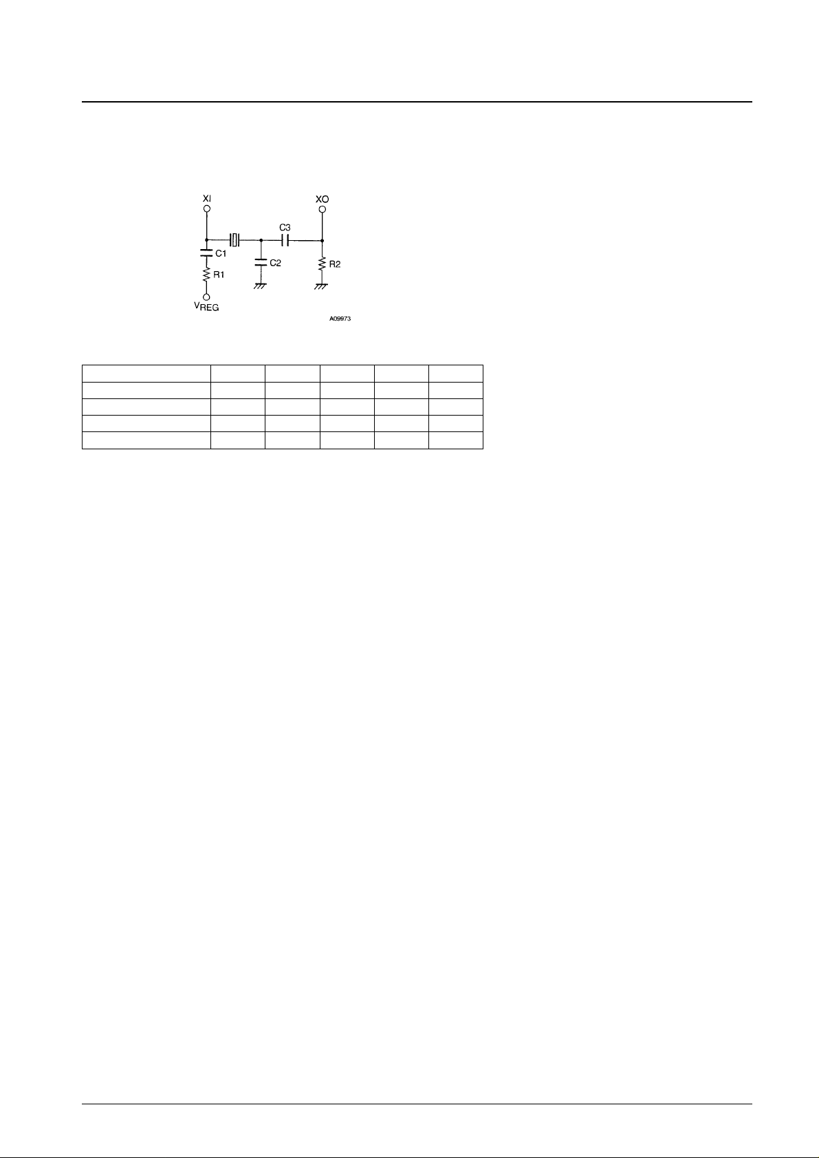
Use the following circuit, consisting of a crystal element, capacitors, and resistors, as a crystal oscillator circuit.
C1 and R1: Used for oscillator stabilization.
C3: Used for oscillator element coupling.
C2: Used for overtone prevention.
R2: Improves the oscillator margin.
This circuit and these component values are only provided for reference purposes. Consult with the manufacturer of
the crystal element concerning the influence of such factors as the characteristics of the crystal element itself and the
stray capacitances due to the printed circuit board wiring pattern to assure that problems do not occur.
(Notes on printed circuit board wiring)
Since crystal oscillator circuits are high-frequency circuits, they are easily influenced by stray capacitances due to the
printed circuit board wiring. Therefore, lines for external components must be kept as short as possible and lines must
be made as narrow as possible. In this external circuit, the connection between the oscillator element and C3 (and C2)
is particularly subject to influence by stray capacitance, and requires special care.
• External clock (crystal oscillator equivalent: a few MHz)
If a signal equivalent to a crystal oscillator signal is input from an external signal generator, input that signal
through a series resistor of about 13 kΩ to the XI pin. Leave the XO pin open.
• External clock (FG frequency equivalent: a few kHz)
If a signal equivalent to the FG frequency is input from an external signal generator, set the N2 pin to the middle
level (or open) and input that signal to the N1 pin. In this case, the motor will remain in the stopped state (shortcircuit braking operation) even if a start input is applied when no clock is input. However, since IC heating due to
the large output drive currents that flow in the short braking state (since the lower side transistors in all phases are
driven) care is required if the braking state must be held for extended periods.
5. Hall input signals
Even if the amplitude of the Hall sensor input signals is changed by the motor, the influence on the output will be
suppressed by the AGC circuit. However, if there are discrepancies between the amplitudes of the three phases, the
output phase switching timing may be shifted.
The output current will be cut off by a protection circuit if a start signal is input when there are no signals applied to
the Hall inputs.
The maximum operating frequency of the Hall inputs is affected by the saturation state of the outputs. While there are
no problems for frequencies of under 1 kHz (the frequency in a single Hall phase), if a higher operating frequency is
required, it can be advantageous if the outputs remain unsaturated. If the outputs remain in the unsaturated state, this
IC can be used up to frequencies of about 2 kHz.
Since motors with higher speeds have higher operating frequencies, we recommend using motors with four motor
magnet poles.
6. LD output
The LD output goes on when the phase is locked. Phase lock is determined not by the speed error but by the phase
error only. Therefore, the speed error when the LD output is on, during, for example, lock pull-in, will change with
the acceleration of the FD signal. (The speed error will be smaller for lower accelerations.) If it is necessary to
No. 5625-10/11
LB1872
Sample External Component Values
Oscillator frequency (MHz) C1 (µF) C2 (pF) C3 (pF) R1 (Ω) R2 (Ω)
1 to 3 0.1 47 220 220 k —
3 to 5 0.1 18 100 100 k —
5 to 7 0.1 — 47 47 k —
7 to 10 0.1 — 33 10 k 4.7 k
Page 11

PS No. 5625-11/11
LB1872
stipulate the speed error when the LD output is on, this must be determined based on the result of a speed
measurement for the motor state.
This IC includes a built-in circuit that masks LD output chattering (rapid switching between on and off) during phase
lock pull-in. The mask time is determined as shown below by the capacitance of the capacitor inserted between the
CLD pin and ground.
t = 0.35 × C
t: Mask time (s)
C: External capacitance (µF)
If LD chattering is masked, the LD output is delayed by the mask time. Therefore care is required, since the speed
error when LD is on is changed by the mask time.
Leave the CLD pin open if there is no need for masking.
7. Power supply stabilization
Since this IC provides large output currents, it can easily cause fluctuations in the power supply line voltage.
Therefore, capacitors with adequate capacitances for stabilization must be inserted between the VDDand ground pins.
If diodes are inserted in the power supply lines to prevent device destruction by reverse power supply connection, the
power supply line voltage becomes especially liable to fluctuations. In this case, even larger capacitors are required.
8. External protection circuits
If an application will include external motor constraint protection and other external protection circuits, use an open
collector transistor output to set the FC pin low to shut off the IC drive current.
This catalog provides information as of January, 1998. Specifications and information herein are subject to
change without notice.
■ No products described or contained herein are intended for use in surgical implants, life-support systems, aerospace
equipment, nuclear power control systems, vehicles, disaster/crime-prevention equipment and the like, the failure of
which may directly or indirectly cause injury, death or property loss.
■ Anyone purchasing any products described or contained herein for an above-mentioned use shall:
➀ Accept full responsibility and indemnify and defend SANYO ELECTRIC CO., LTD., its affiliates, subsidiaries and
distributors and all their officers and employees, jointly and severally, against any and all claims and litigation and all
damages, cost and expenses associated with such use:
➁ Not impose any responsibility for any fault or negligence which may be cited in any such claim or litigation on
SANYO ELECTRIC CO., LTD., its affiliates, subsidiaries and distributors or any of their officers and employees
jointly or severally.
■ Information (including circuit diagrams and circuit parameters) herein is for example only; it is not guaranteed for
volume production. SANYO believes information herein is accurate and reliable, but no guarantees are made or implied
regarding its use or any infringements of intellectual property rights or other rights of third parties.
 Loading...