

Page 1

Monolithic Digital IC
Ordering number : EN4476B
O3097HA (OT)/31795TH (OT) No. 4476-1/6
SANYO Electric Co.,Ltd. Semiconductor Bussiness Headquarters
TOKYO OFFICE Tokyo Bldg., 1-10, 1 Chome, Ueno, Taito-ku, TOKYO, 110 JAPAN
Three-Phase Brushless Motor Driver IC
LB1854M
Overview
The LB1854M is a three-phase brushless motor driver IC
and is optimal, in particular, for driving VCR capstan and
drum motors.
Features
• 120° voltage linear drive technique
• The LB1854M soft switching scheme allows smaller
external capacitors to be used (e.g., chip capacitors).
• Built-in thermal-shutdown function
• Built-in overcurrent protection circuit
• Built-in FG amplifiers (operational amplifier and
Schmitt amplifier)
• Control start voltage set by an external voltage
• The output current feedback level can be changed by
changing the control gain to one of two levels.
Package Dimensions
unit: mm
3073A-MFP30S
SANYO: MFP30S
[LB1854M]
Specifications
Absolute Maximum Ratings at Ta = 25°C
Allowable Operating Ranges at Ta = 25°C
Parameter Symbol Conditions Ratings Unit
Maximum supply voltage
V
CC
1 max 20 V
V
CC
2 max 7.0 V
Applied output voltage V
OU, V, W
22 V
Maximum output current I
OUT
max 1.5 A
Allowable power dissipation Pd max 1.05 W
Operating temperature Topr –20 to +75 °C
Storage temperature Tstg –55 to +150 °C
Parameter Symbol Conditions Ratings Unit
Supply voltage
V
CC
1 5 to 18 V
V
CC
2 4.3 to 6.5 V
Page 2

No. 4476-2/6
LB1854M
Electrical Characteristics at Ta = 25°C, VCC1 = 12 V, VCC2 = 5 V
Note: * Items marked with an asterisk are design target values and are not measured.
Parameter Symbol Conditions min typ max Unit
Current drain
I
CC
1 VC= 0 V, RL= ∞ 17 30 mA
I
CC
2 VC= 0 V 6.5 9.5 mA
[Drive Block]
Output saturation voltage
V
O
(sat) 1 I
OUT
= 0.5 A, sink + source 1.6 2.2 V
V
O
(sat) 2 I
OUT
= 1.0 A, sink + source 2.0 3.0 V
Output TRS breakdown voltage V
O
(sus) I
OUT
= 20 mA* 20 V
Output resting potential V
OQ
VC= 0 V 5.7 6.0 6.3 V
Hall amplifier input offset voltage V
H
offset –5 +5 mV
Hall amplifier input bias current I
H
bias 1 5 µA
Hall amplifier common mode
V
H
ch 1.3 2.2 V
input voltage range
Hall input/output voltage gain GV
HO
43 46 49 dB
[Control Block]
Control output drive gain
GV
CO
1 High gain 37 40 43 dB
GV
CO
2 Low gain 31 34 37 dB
Control output CH difference ∆GV
CO
–2 +2 dB
Control start voltage V
CTH
When V
OUT
p-p = 2 V 2.5 V
Gain control switching high level 4 5 V
Gain control switching
Middle level when the input is open 2 3 V
middle level
Gain control switching low level 0 1 V
[FG Amplifier]
FG amplifier input offset voltage V
FG
offset –8 +8 mV
Open-loop voltage gain GV
FG
f = 1 kHz 60 dB
Source output saturation voltage V
FG OUIO
= 2 mA 37 V
Sink output saturation voltage V
FG ODIO
= –2 mA 1.3 V
Common-mode signal
CHR
*
80 dB
rejection ratio
FG amplifier common-mode
V
FG CH
0 3.5 V
input voltage range
Phase margin * 20 Deg
Schmitt hysteresis
∆Vsh1 FG
OUT
2: High to low 22 mV
∆Vsh2 FG
OUT
2: Low to high 22 mV
Schmitt input voltage range Vsh
CH
0.7 3.5 V
[Thermal Shutdown]
Operating temperature TSD * 150 180 210 °C
Hysteresis ∆TSD * 15 °C
Page 3
No. 4476-3/6
LB1854M
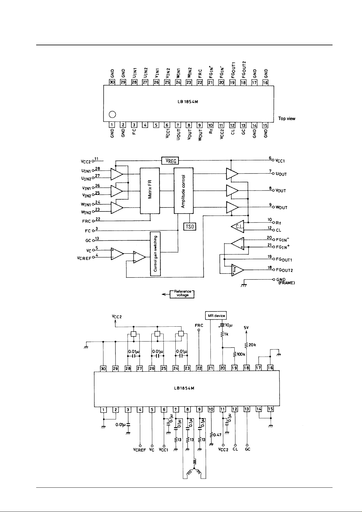
Pin Assignment
Block Diagram
Sample Application Circuit
Unit (resistance: Ω, capacitance: F)
V
CREF
V
C
Page 4
No. 4476-4/6
LB1854M
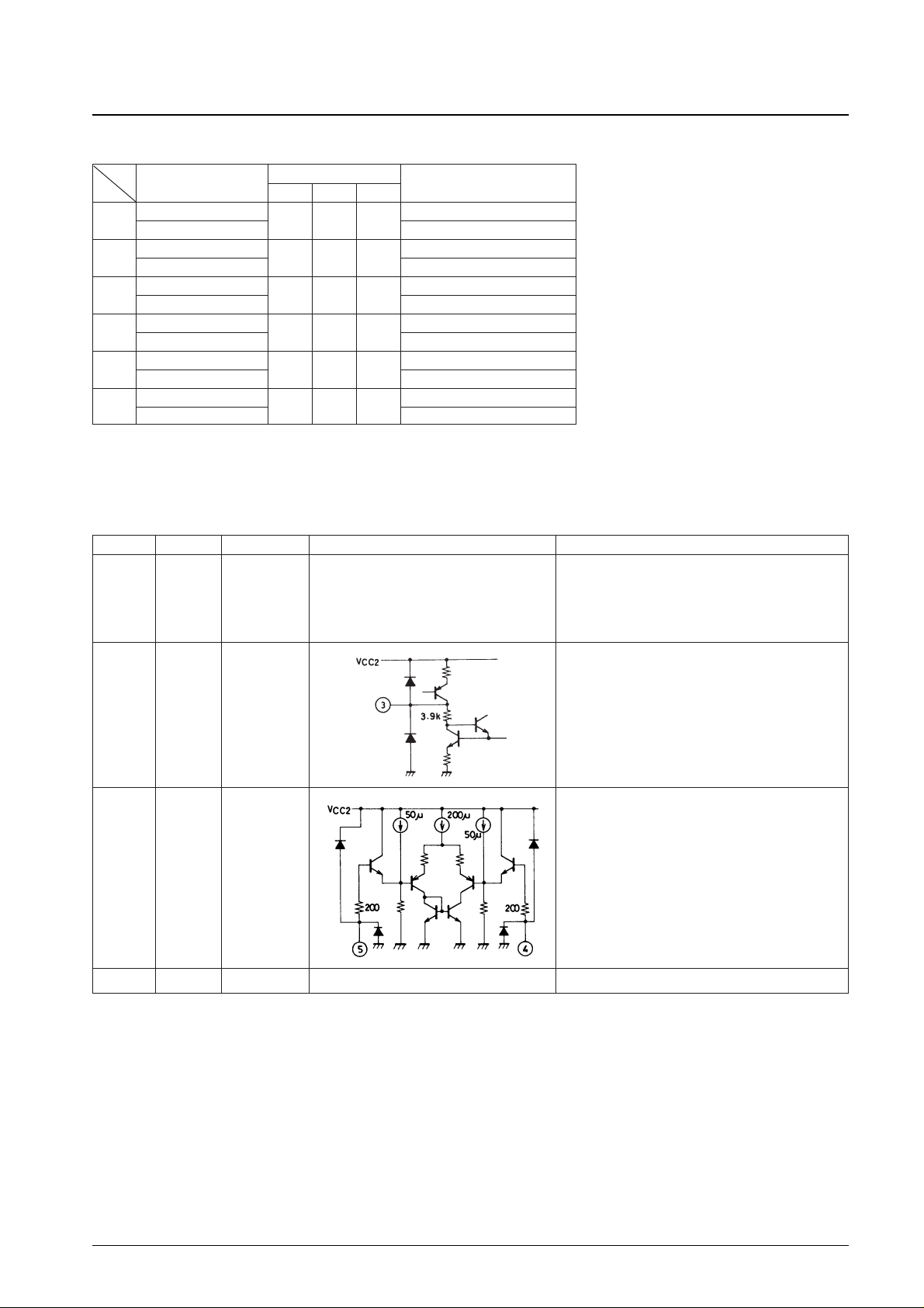
Truth Table
Input high: Phase 1 is 0.2 V or more higher than the corresponding phase 2 for each phase input.
Low: Phase 1 is 0.2 V or more lower than the corresponding phase 2 for each phase input.
Forward and reverse control high: 2.3 V to V
CC
1
Low: 0 V to 0.7 V
Pin Functions
Unit (resistance: Ω)
Source
Input
Forward and reverse control
Sink
U V W
F/RC
1
W phase
→ V phase
H H L
L
V phase → W phase H
2
W phase → U phase
H L L
L
U phase → W phase H
3
V phase → W phase
L L H
L
W phase → V phase H
4
U phase → V phase
L H L
L
V phase → U phase H
5
V phase → U phase
H L H
L
U phase → V phase H
6
U phase → W phase
L H H
L
W phase → U phase H
Pin No. Symbol Pin voltage Equivalent circuit Function
1, 2, 14,
15, 16,
17, 29,
30
3
4
5
6
FRAME
(GND)
FC
V
C REF
V
C
VCC1
1.5 V min
V
CC
2 max
0 V min
VCC2 max
5 to 18 V
Ground for all circuits except the outputs
The gain frequency characteristics can be lowered by
connecting a capacitor between this pin and ground to
prevent oscillation.
Speed control
The LB1854M implements a voltage control scheme in
which the output voltage is controlled by the pin 5 voltage.
The pin 4 voltage determines the control start voltage.
Power supply that provides the drive outputs
Page 5
No. 4476-5/6
LB1854M
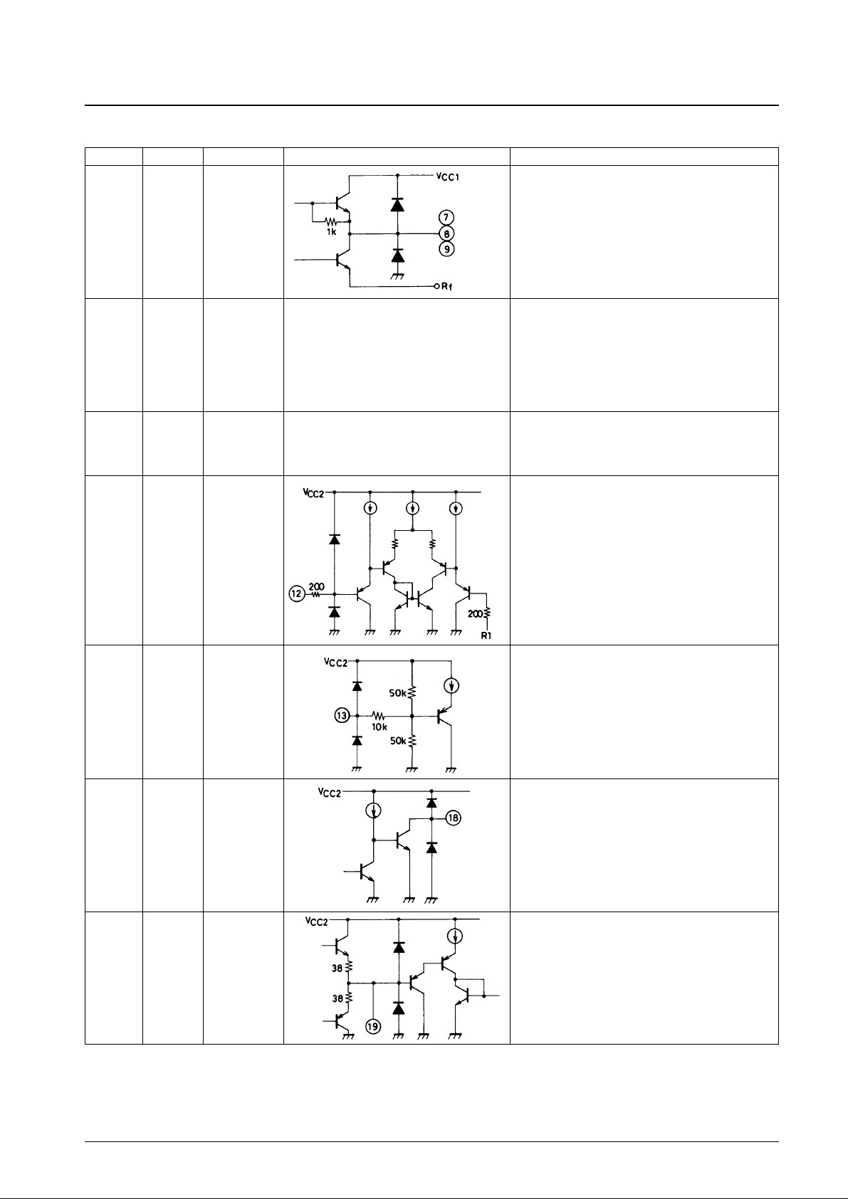
Continued from preceding page.
Unit (resistance: Ω)
Pin No. Symbol Pin voltage Equivalent circuit Function
7
8
9
10
11
12
13
18
19
U
OUT
V
OUT
W
OUT
R
f
VCC2
CL
GC
FG
OUT
2
FG
OUT
1
4.3 to 6.5 V
0 V min
V
CC
2 max
0 V min
V
CC
2 max
Output pins
Output transistor ground
Feedback can be applied to the control amplifier by
inserting resistor between this pin and GND and detecting
the output current as a voltage. The overcurrent
protection circuit (current limiter) operates by detecting
the voltage on this pin.
Power supply provided to all blocks other than the output
block
This voltage must be stabilized so that no ripple or other
noise is present.
The current limiter operates when the R
f
pin reaches the
same potential as pin 12. The pin 12 potential is set up
externally.
Control input to output gain switching pin
High level (4 to 5 V): 34 dB
Middle level (2 to 3 V) or open: 40 dB (low speed):
34 dB (high speed)
Low level (0 to 1 V): 40 dB
However, note that this applies when V
CC
2 is 5 V.
FG Schmitt amplifier output
FG amplifier output
Continued on next page.
Page 6
No. 4476-6/6
LB1854M
This catalog provides information as of November, 1997. Specifications and information herein are subject to
change without notice.
■ No products described or contained herein are intended for use in surgical implants, life-support systems, aerospace
equipment, nuclear power control systems, vehicles, disaster/crime-prevention equipment and the like, the failure of
which may directly or indirectly cause injury, death or property loss.
■ Anyone purchasing any products described or contained herein for an above-mentioned use shall:
➀ Accept full responsibility and indemnify and defend SANYO ELECTRIC CO., LTD., its affiliates, subsidiaries and
distributors and all their officers and employees, jointly and severally, against any and all claims and litigation and all
damages, cost and expenses associated with such use:
➁ Not impose any responsibility for any fault or negligence which may be cited in any such claim or litigation on
SANYO ELECTRIC CO., LTD., its affiliates, subsidiaries and distributors or any of their officers and employees
jointly or severally.
■ Information (including circuit diagrams and circuit parameters) herein is for example only; it is not guaranteed for
volume production. SANYO believes information herein is accurate and reliable, but no guarantees are made or implied
regarding its use or any infringements of intellectual property rights or other rights of third parties.
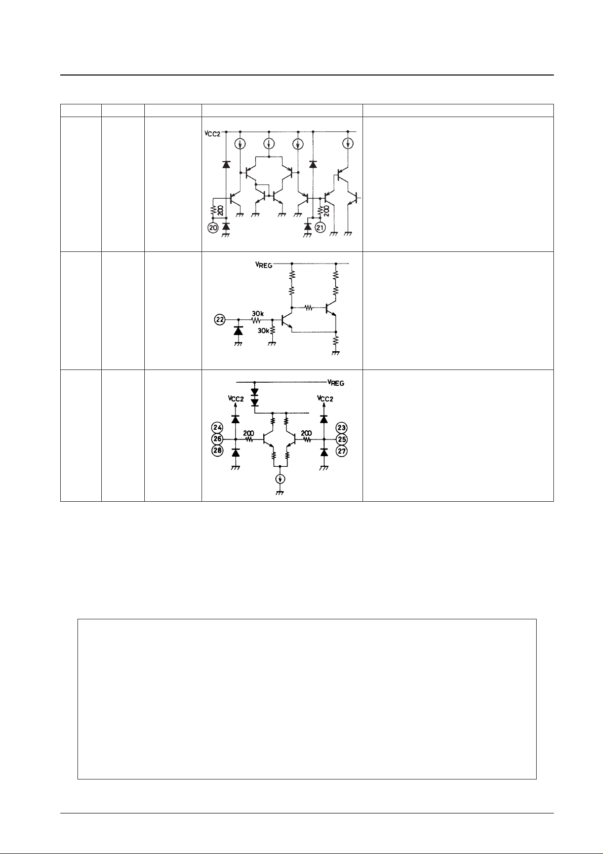
Continued from preceding page.
Unit (resistance: Ω)
Pin No. Symbol Pin voltage Equivalent circuit Function
20
21
22
23
24
25
26
27
28
FG
IN
–
FG
IN
+
FRC
W
IN
2
W
IN
1
V
IN
2
V
IN
1
U
IN
2
U
IN
1
0 V min
3.5 V max
(when V
CC
2 is
5 V)
High: 2.3 V min
Low: 0.7 V max
1.4 V min
2.0 V max
FG signal input
Motor forward/reverse control pin
Low level (0.7 V or lower): forward
High level (2.3 V or higher): reverse
W phase Hall sensor input
Logic high is the W
IN
1 > WIN2 state.
V phase Hall sensor input
Logic high is the VIN1 > VIN2 state.
U phase Hall sensor input
Logic high is the UIN1 > UIN2 state.
 Loading...