

Page 1

Overview
The LB1821M is a pre-driver IC that supports direct
PWM drive and is appropriate for the power brushless
motors used in office automation equipment. A motor
drive circuit with the desired output capability (voltage
and current characteristics) can be constructed by
attaching a driver array at the IC output. The LB1821M
includes on chip a speed control circuit that allows the
motor speed to be varied using an external clock.
Features
• Direct PWM drive output
• Speed discriminator + PLL speed control circuit
• FG and integrating amplifiers
• Forward/reverse switching circuit
• Braking circuit (short braking)
• Speed lock detection output
• Full complement of on-chip protection circuits,
including lock protection, current limiter, and
thermal shutdown protection circuits.
Package Dimensions
unit: mm
3148-QFP44MA
Monolithic Digital IC
Ordering number : EN5686
63097HA(OT) No. 5686-1/16
SANYO: QIP44MA
[LB1821M]
SANYO Electric Co.,Ltd. Semiconductor Bussiness Headquarters
TOKYO OFFICE Tokyo Bldg., 1-10, 1 Chome, Ueno, Taito-ku, TOKYO, 110 JAPAN
Power Brushless Motor Pre-Driver IC
for OA Equipment
LB1821M
Parameter Symbol Conditions Ratings Unit
Maximum supply voltage V
CC
max 9V
Maximum input current I
REG
max V
REG
pin 10 mA
Output current I
O
max UL, UV, and WL outputs 30 mA
Allowable power dissipation Pd max 0.9 W
Operating temperature Topr –20 to +80 °C
Storage temperature Tstg –55 to +150 °C
Specifications
Absolute Maximum Ratings at Ta = 25°C
Parameter Symbol Conditions Ratings Unit
Supply voltage V
CC
4.4 to 7.0 V
Input current range I
REG
V
REG
pin (7 V) 1 to 5 mA
FG Schmitt output applied voltage V
FGS
0 to 8 V
FG Schmitt output current I
FGS
0 to 5 mA
Lock detection output current I
LD
0 to 20 mA
Allowable Operating Ranges at Ta = 25°C
Page 2

No. 5686-2/16
LB1821M
Parameter Symbol Conditions
Ratings
Unit
min typ max
I
CC
1 42 60 mA
Current drain
I
CC
2 In stop mode 10 20 mA
I
CC
3 VCC= 5 V 38 55 mA
I
CC
4 VCC= 5 V, In stop mode 8 18 mA
Output saturation voltage V
O
(sat) UL, VL, WL output, IO= 20 mA 0.2 0.7 V
Output current I
O
UH, VH, WH output, V
OUT
= 1.4 V –20 –16 –12 mA
Output leakage current I
O
leak UL, VL, WL output 100 µA
Output off voltage V
O
off UH, Vh, WH output 0.5 V
[Hall Amplifier]
Input bias current I
HB(HA)
–4 –1 µA
Common-mode input voltage range V
ICM
1.5 V
CC
– 1.5 V
Hall input sensitivity ∆V
IN(HA)
60 mVp-p
Hysteresis ∆V
IN(HA)
17 32 60 mV
Input voltage low
→ high V
SLH
8 16 30 mV
Input voltage high → low V
SHL
–30 –16 –8 mV
[RC Oscillator]
Output high-level voltage
V
OH(CR)
1 3.1 3.4 3.7 V
V
OH(CR)
2 VCC= 5 V 2.4 2.7 3.0 V
Output low-level voltage
V
OL(CR)
1 1.5 1.8 2.1 V
V
OL(CR)
2 VCC= 5 V 1.1 1.4 1.7 V
Oscillator frequency f
(CR)
R = 75 kΩ, C = 1500 pF 19 kHz
Amplitude
V
(CR)
1 1.4 1.6 1.8 Vp-p
V
(CR)
2 VCC= 5 V 1.1 1.3 1.5 Vp-p
[CROCK Oscillator]
Output high-level voltage
V
OH(RK)
1 3.2 3.5 3.8 V
V
OH(RK)
2 VCC= 5 V 2.5 2.8 3.1 V
Output low-level voltage
V
OL(RK)
1 0.8 1.1 1.4 V
V
OL(RK)
2 VCC= 5 V 0.6 0.9 1.2 V
External capacitor charge current I
CHG
1 –17 –13 –9 µA
External capacitor discharge current I
CHG
2 9 13 17 µA
Oscillator frequency f
(RK)
C = 0.068 µF 35 Hz
Amplitude
V
(RK)
1 2.2 2.4 2.6 Vp-p
V
(RK)
2 VCC= 5 V 1.7 1.9 2.1 Vp-p
Electrical Characteristics at Ta = 25°C, VCC= 6.3 V
Continued on next page.
Allowable power dissipation, Pdmax – W
Ambient temperature, Ta – °C
Page 3

No. 5686-3/16
LB1821M
Parameter Symbol Conditions
Ratings
Unit
min typ max
[VCO Oscillator]
Pin C output high-level voltage
V
OH(C)
1 4.1 4.3 4.6 V
V
OH(C)
2 VCC= 5 V 3.2 3.4 3.6 V
Pin C output low-level voltage
V
OL(C)
1 3.6 3.9 4.1 V
V
OL(C)
2 VCC= 5 V 2.8 3.0 3.2 V
Oscillator frequency f
(C)
1.0 MHz
Amplitude V
(C)
0.2 0.4 0.6 Vp-p
[Current Limiter Operation]
Limiter V
RF
0.47 0.52 0.57 V
[Thermal Shutdown Operation]
Thermal shutdown operating temperature TSD Design target value 150 180 °C
Hysteresis ∆TSD Design target value 30 °C
V
REG
pin voltage V
REG
6.6 7.0 7.3 V
[FG Amplifier]
Input offset voltage V
IO(FG)
–10 +10 mV
Input bias current I
B(FG)
–1 +1 µA
Output high-level voltage V
OH(FG)
VCC– 1.5 VCC– 1 V
Output low-level voltage V
OL(FG)
1 1.5 V
FG input sensitivity Gain: 100× 3 mV
Schmitt amplitude for the next stage 100 180 250 mV
Operating frequency range 16 kHz
Open-loop gain f
(FG)
= 2 kHz 45 51 dB
[FGS Output]
Output saturation voltage V
O(FGS)IO(FGS)
= 2 mA 0.1 0.5 V
Output leakage current I
L(FGS)VO
= V
CC
10 µA
[Speed Discriminator Output]
Output high-level voltage V
OH(D)
VCC– 1.0 VCC– 0.7 V
Output low-level voltage V
OL(D)
0.4 1.1 V
[Speed Control PLL Output]
Output high-level voltage
V
OH(P)
1 4.05 4.35 4.65 V
V
OH(P)
2 VCC= 5 V 3.25 3.55 3.83 V
Output low-level voltage
V
OL(P)
1 1.85 2.15 2.45 V
V
OL(P)
2 VCC= 5 V 1.25 1.55 1.85 V
[VCO PLL Output]
Output high-level voltage V
OH(VCO)
5.3 5.6 V
Output low-level voltage V
OL(VCO)
0.4 11 V
[Lock Detection]
Output saturation voltage V
OL(LD)ILD
= 10 mA 0.1 0.5 V
Output leakage current I
L(LD)VO
= V
CC
10 µA
Lock range –6.25 +6.25 %
[Integrator]
Input offset voltage V
IO(INT)
–10 10 mV
Input bias current I
B(INT)
–0.4 +0.4 µA
Output high-level voltage V
OH(INT)
VCC– 1.2 VCC– 0.8 V
Output low-level voltage V
OL(INT)
0.8 1.2 V
Open-loop gain 60 dB
Input bias current 1.6 MHz
Gain-bandwidth product
Reference voltage V
B(INT)
–5% VCC/2 5% V
[Filter Amplifier]
Input bias current I
B(FIL)
–0.4 +0.4 µA
Output high-level voltage V
OH(FIL)
VCC– 1.2 VCC– 0.8 V
Output low-level voltage V
OL(FIL)
0.8 1.2 V
Reference voltage
V
B(FIL)
1 –5% 2.0 5% V
V
B(FIL)
2 VCC= 5 V 1.5 1.6 1.7 V
Continued from preceding page.
Continued on next page.
Page 4

No. 5686-4/16
LB1821M
Parameter Symbol Conditions
Ratings
Unit
min typ max
[S/S Pin]
Output high-level voltage V
OH(S/S)
4.0 V
CC
V
Output low-level voltage V
OL(S/S)
0 1.5 V
Hysteresis
∆V
IN(S/S)
1 0.35 0.45 0.55 V
∆V
IN(S/S)
2 VCC= 5 V 0.24 0.34 0.44 V
Pull-up resistance R
U(S/S)
45 63 85 kΩ
[F/R Pin]
Input high-level voltage V
IH(F/R)
4.0 V
CC
V
Input low-level voltage V
IL(F/R)
0 1.5 V
Hysteresis
∆V
IN(F/R)
1 0.35 0.45 0.55 V
∆V
IN(F/R)
2 VCC= 5 V 0.24 0.34 0.44 V
Pull-up resistance R
U(F/R)
45 63 85 kΩ
[BR Pin]
Input high-level voltage V
IH(BR)
4.0 V
CC
V
Input low-level voltage V
IL(BR)
0 1.5 V
Hysteresis
∆V
IN(BR)
1 0.35 0.45 0.55 V
∆V
IN(BR)
2 VCC= 5 V 0.24 0.34 0.44 V
Pull-up resistance R
U(BR)
45 63 85 kΩ
[CLK Pin]
Input high-level voltage V
IH(CLK)
Design target value 4.0 V
CC
V
Input low-level voltage V
IL(CLK)
Design target value 0 1.5 V
Hysteresis
∆V
IN(CLK)
1 Design target value 0.35 0.45 0.55 V
∆V
IN(CLK)
2 VCC= 5 V, Design target value 0.24 0.34 0.44 V
Pull-up resistance R
U(CLK)
45 63 85 kΩ
Input frequency f
(CLK)
[N1 Pin]
Input high-level voltage V
IH(N1)
4.0 V
CC
V
Input low-level voltage V
IL(N1)
0 1.5 V
Hysteresis
∆V
IN(N1)
1 0.35 0.45 0.55 V
∆V
IN(N1)
2 VCC= 5 V 0.24 0.34 0.44 V
Pull-up resistance R
U(N1)
45 63 85 kΩ
[N2 Pin]
Input high-level voltage V
IH(N2)
4.0 V
CC
V
Input low-level voltage V
IL(N2)
0 1.5 V
Hysteresis
∆V
IN(N2)
1 0.35 0.45 0.55 V
∆V
IN(N2)
2 VCC= 5 V 0.24 0.34 0.44 V
Pull-up resistance R
U(N2)
45 63 85 kΩ
[Low Voltage Protection]
Operating voltage V
SDL
3.75 V
Release voltage V
SDH
4.0 V
Hysteresis ∆V
SD
0.15 0.25 0.35 V
Continued from preceding page.
Speed Discriminator Counts
N1 N2 Number of counts
High or open High or open 64
High or open L 256
L High or open 128
L L 512
Page 5

No. 5686-5/16
LB1821M
Three-Phase Logic Truth Table (A high (H) input is the state where IN+> IN–.)
Item
F / R = L F / R = H Output
IN1 IN2 IN3 IN1 IN2 IN3 Source Sink
1 H L H L H L VH UL
2 H L L L H H WH UL
3 H H L L L H WH VL
4 L H L H L H UH VL
5 L H H H L L UH WL
6 L L H H H L VH WL
S/S Pin
Pin Assignment
High or open Stop
L Start
BRK Pin
High or open Brake
L Released
Page 6
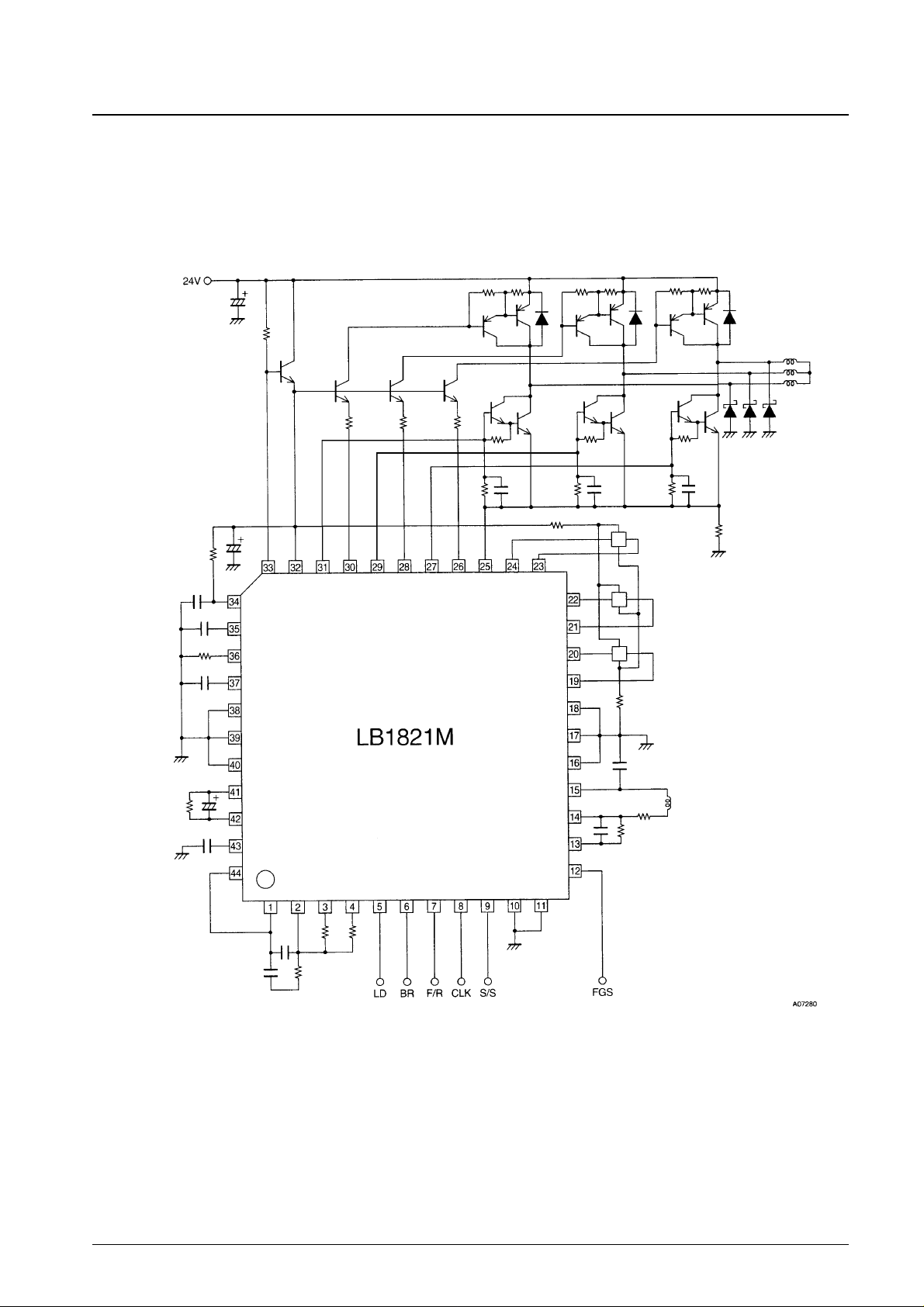
Sample Application Circuit
No. 5686-6/16
LB1821M
Page 7
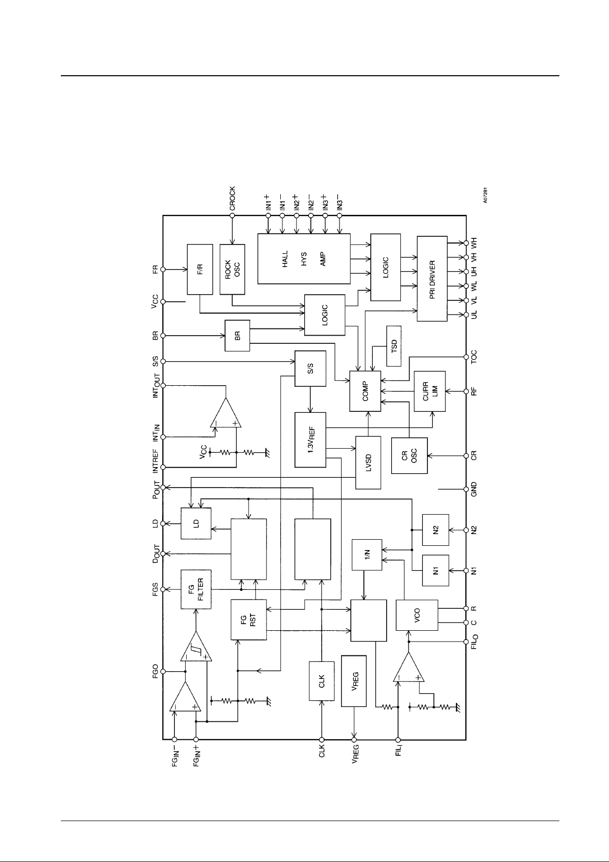
Internal Equivalent Circuit Block Diagram
No. 5686-7/16
LB1821M
Speed
discriminator
Speed control
system PLL
VCO
system PLL
Page 8
IC Operation Description
1. Speed Control Circuit
This IC implements speed control using the combination of a speed discriminator circuit and a PLL circuit. The speed
discriminator and the PLL circuit output (using a charge pump technique) an error signal once every two FG periods.
As compared to the earlier technique in which only a speed discriminator circuit was used, the combination of a
speed discriminator and a PLL circuit allows variations in motor speed to be better suppressed when a motor that has
large load variations is used. The FG servo frequency is controlled to be the same frequency as the clock signal input
to the CLK pin. This means that the motor speed can be changed by changing the clock frequency.
2. VCO Circuit
The LB1821M includes an on-chip VCO circuit to generate the reference signal for the speed discriminator circuit.
The reference signal frequency is determined by the following formula.
f
VCO
= f
CLK
× number of counts
f
VCO
: Reference signal frequency
f
CLK
: Frequency of the externally input clock signal
The range over which the reference signal can be varied is determined by the resistor and capacitor connected to the
R pin (pin 36) and the C pin (pin 37) and by the VCO loop filter constants (the external constants connected to pins
41 and 42).
(Reference Values)
The value of R must not be less than 2.7 kΩ.
Applications can handle a wider range of speed variations than would be possible if a fixed number of counts was
used by changing the number of discriminator counts (which is related to the divisor in the VCO circuit). The number
of counts can be switched between 64, 128, 256, and 512 by setting the N1 (pin 10) and N2 (pin 11) pins.
3. Output Drive Circuit
To reduce power loss in the output, this IC adopts the direct PWM drive technique. The output transistors (which are
external to the IC) are always saturated when on, and the motor drive output is adjusted by changing the duty with
which the output is on. Since the (external) output switching is handled by the upper side output transistors, a
Schottky diode or similar device must be connected between the output (OUT) and ground. This is because a through
current will flows at the instant the upper side output transistors turn on if a diode with a short reverse recovery time
is not used. A rectifying diode can be used between OUT and VCC. Transistors that have no parasitic diodes must be
used for the lower side output transistors. If these transistors have parasitic diode components, then through currents
will occur due to the reverse recovery time of the parasitic diodes despite the inclusion of the external Schottky
diodes.
4. Current Limiter Circuit
The current limiter circuit limits the (peak) current at the value I = VRF/Rf(VRF= 0.52 V (typical), Rf: current
detection resistor). The current limitation operation consists of reducing the output duty to suppress the current.
5. Speed Lock Range
The speed lock range is ±6.25% of the fixed speed. When the motor speed is in the lock range, the LD pin (an open
collector output) goes low. If the motor speed goes out of the lock range, the motor on duty is adjusted according to
the speed error to control the motor speed to be within the lock range. Caution is required, since the LD signal may
go on initially at startup. (It will be low while two or three FG signal pulses are input.)
6. Notes on the PWM Frequency
The PWM frequency is determined by the resistor and capacitor connected to the CR pin.
f
PWM
≈ 1/(0.48 × C × R)
A PWM frequency of between 15 and 25 kHz is desirable. If the PWM frequency is too low, the motor may resonate
No. 5686-8/16
LB1821M
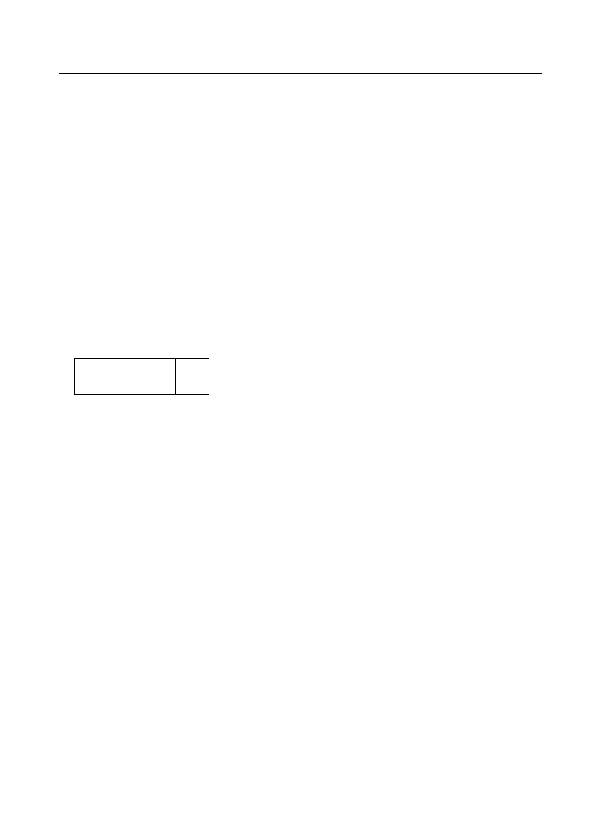
Supply voltage R (kΩ) C (pF)
V
CC
= 5 V 4.7 390
V
CC
= 6.3 V 4.7 820
Page 9

at the PWM frequency during motor control, and if that frequency is in the audible range, that resonation may result
in audible noise. If the PWM frequency is too high, the output transistor switching loss will increase. The external
resistor must not have a value under 30 kΩ.
7. Hall Input Signals
Input signals with an amplitude greater than the hysteresis (60 mV, maximum) are required for the Hall inputs. An
input amplitude of 100 mV or greater is desirable, taking noise and other considerations into account. The Hall input
DC voltage must be set to fall within the common-mode input voltage range specifications.
8. Forward/Reverse (F/R) Switching
The F/R pin can be used to switch the motor direction. The direction can be switched with the F/R pin even if the
motor is turning. The IC circuit is designed to compensate for the through currents that occur when the direction is
switched. However, caution is required with respect to increases in the VCCvoltage (due to motor current returning to
the power system instantaneously) during direction switching. If this is a problem, try increasing the capacitance of
the capacitor connected between the power supply and ground.
9. Brake Switching
The LB1821M implements a short braking technique in which the upper side transistors (the external transistors) for
all phases are turned on. (The lower side transistors for all phases are turned off.) This means that the output current
during braking does not pass through the Rf(the current detection resistor) and therefore that the current limiter does
not function. Thus caution is required. During braking, the upper side transistors operate at a 100% duty, regardless
of the motor speed. The braking function can be operated and released in the start state. Thus motor start and stop
control can be performed from the brake pin with the S/S pin at the low level, i.e., with the system in the start state. If
the startup time is a problem, the motor can be started with a shorter startup time by using the brake pin for motor
start/stop control than it can with the S/S pin. (This is because the stop state is a power saving state, and restarting
from this state requires waiting the time required for the VCO circuit to stabilize.)
10. Constraint Protection Circuit
The LB1821M includes an on-chip constraint protection circuit to protect the IC and the motor in motor constraint
mode. If the LD output remains high (indicating the locked state) for a fixed period in the start state, the upper side
(external) transistors are turned off. This time is set by the capacitance of the capacitor attached to the CROCK pin. A
time of a few seconds can be set with a capacitance of under 0.1 µF.
<Set time (s)> ≈ 44 × C (µF)
To release the constraint protection state, the LB1821M must be set to either the stop state or the brake state, or
power must be reapplied. The CROCK pin must be connected to ground if the constraint protection circuit is not
used. However, note that the clock disconnection protection circuit described later cannot be used in this case.
11. Clock Disconnection Protection Circuit
If clock input stops with the LB1821M in the start state, this protection circuit operates and turns off the (external)
upper side output transistors. If the clock is reapplied, the IC resumes operation.
12. Low-Voltage Protection Circuit
The LB1821M includes a low-voltage protection circuit to protect against incorrect operation when power is first
applied or if the power-supply voltage (VCC) falls. The (external) upper side output transistors are turned off if V
CC
falls under about 3.75 volts, and this function is cleared at about 4.0 volts.
13. Power Supply Stabilization
Since this IC is used in applications that draw large output currents, the power-supply line is subject to fluctuations.
Therefore, capacitors with capacitances adequate to stabilize the power-supply voltage must be connected between
the VCCpin and ground. If diodes are inserted in the power-supply line to prevent IC destruction due to reverse
power supply connection, since this makes the power-supply voltage even more subject to fluctuations, even larger
capacitors will be required.
14. Ground Lines
The signal system ground and the output system ground must be separated and a single ground point must be taken at
the connector. Since the output system ground carries large currents, this ground line must be made as short as
possible.
No. 5686-9/16
LB1821M
Page 10
Output system ground ... Ground for Rfand the output diodes
Signal system ground ... Ground for the IC and the IC external components
15. V
REG
Pin
If a motor drive system is formed from a single power supply, the V
REG
pin (pin 33) can be used to create the power-
supply voltage (about 6.3 V) for this IC. The V
REG
pin is a shunt regulator and generates a voltage of about 7 volts by
passing a current through an external resistor. A stable voltage can be generated by setting the current to value in the
range 1 to 7 mA. The external transistors must have current capacities of at least 80 mA (to cover the ICC+ Hall bias
current + output current <source> requirements) and they must have voltage handling capacities in excess of the
motor power-supply voltage. Since the heat generated by these transistor may be a problem, heat sinks may be
required depending on the packages used. If the IC power-supply voltage (4.4 to 7.0 V) is provided from an external
circuit, apply that voltage directly to the VCCpin(pin 32). In that case, the V
REG
pin must either be left open or
connected to ground.
16. FG Amplifier
Normally, the FG amplifier is used to construct a filter amplifier such as that shown in the application circuit to reject
noise. Since a Schmitt comparator is connected after the FG amplifier, applications must set the amplification so that
the amplifier output amplitude is at least 250 mV p-p. (However, a setting that results in an amplitude of 1 to 3 V p-p
during steady-state rotation is desirable.) The capacitor connected between the FGIN+ pin (pin 15) and ground is
required for bias voltage stabilization and to generate the initial reset pulse for the internal logic. The reset pulse is
generated in the time it takes for the FGIN+ pin to go from 0 to about 1.3 V.
17. Integrating Amplifier
The integrating amplifier integrates the speed error pulses and the phase error pulses and converts them to a speed
command voltage. At the same time it also sets the control loop gain and frequency characteristics using external
components. The integrating amplifier output (pin 1) is normally connected to the TOC pin (pin 44) by an external
line. Separating the integrating amplifier output and the PWM control circuit allows applications to switch the
integrating amplifier constants using an external operational amplifier, analog switch, or other circuit. This is useful
in applications that require integration constant switching due to a wide range of variability in the motor speeds that
must be provided.
18. VCO Filter Amplifier
The VCO filter amplifier converts the VCO system PLL output to the VCO voltage. The amplifier input resistor
(about 10 kΩ) is built in. Therefore, the gain and the frequency characteristics are set by the feedback resistor and the
feedback capacitor. Since the range of frequency variation supported becomes narrower as the gain is reduced, it is
desirable to set the gain of this amplifier to be 1 or higher.
19. Startup Techniques
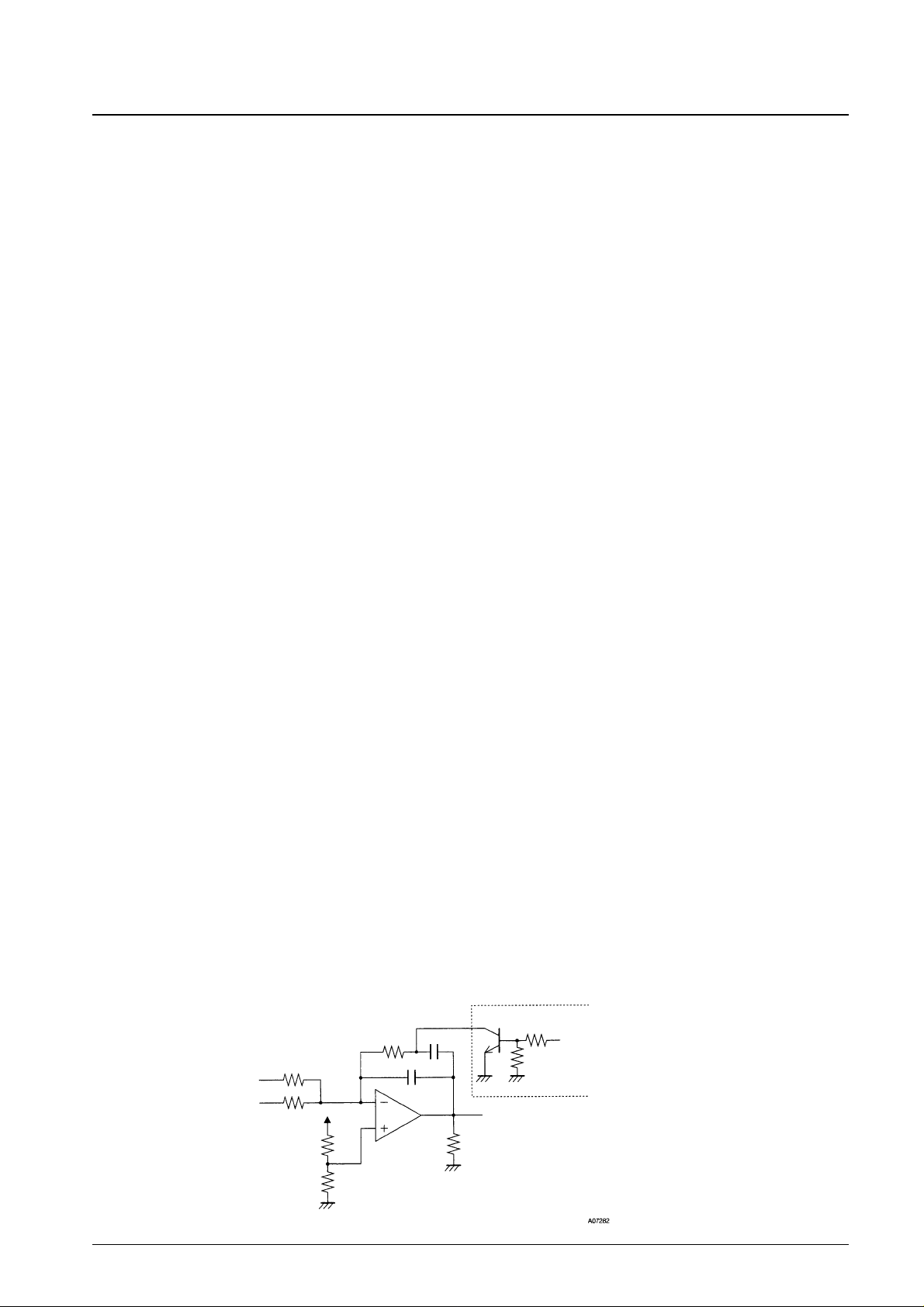
If the motor is started and stopped repeatedly over a short period, the charge accumulated on the integrating
amplifier’s external capacitor may become a problem. (This can result in abnormal speed overshooting at startup and
other problems.) The circuit shown below can be effective at resolving this problem.
No. 5686-10/16
LB1821M
Added circuit
S/S signal
Page 11
No. 5686-11/16
LB1821M
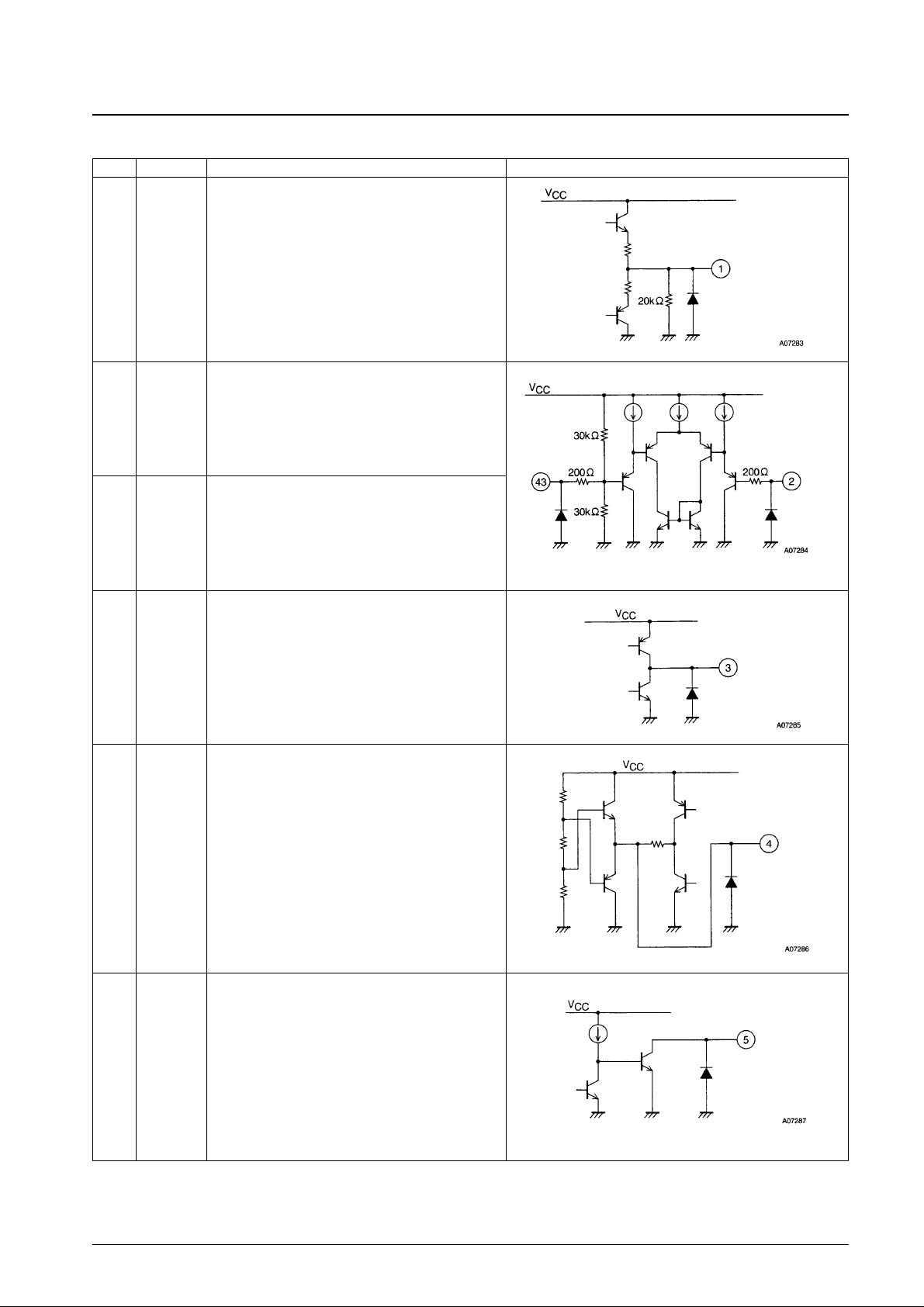
Pin No. Pin Functions Equivalent circuit
Pin Functions
1
INT
OUT
Integrating amplifier output (speed control)
2
INT
IN
Integrating amplifier inverting input
43 INTREF
Integrating amplifier noninverting input
(a potential of 1/2 V
CC
)
3
D
OUT
Speed discriminator output
Outputs a low level for over speed.
Acceleration → high, deceleration → low
4
P
OUT
Speed control system PLL output
Outputs the phase comparison result for
1/2 f
CLK
and 1/2 fFG.
5 LD
Speed lock detection output
Open collector output
Goes low when the motor speed is within the speed lock
range (±6.25%).
Continued on next page.
Page 12
No. 5686-12/16
LB1821M
Continued from preceding page.
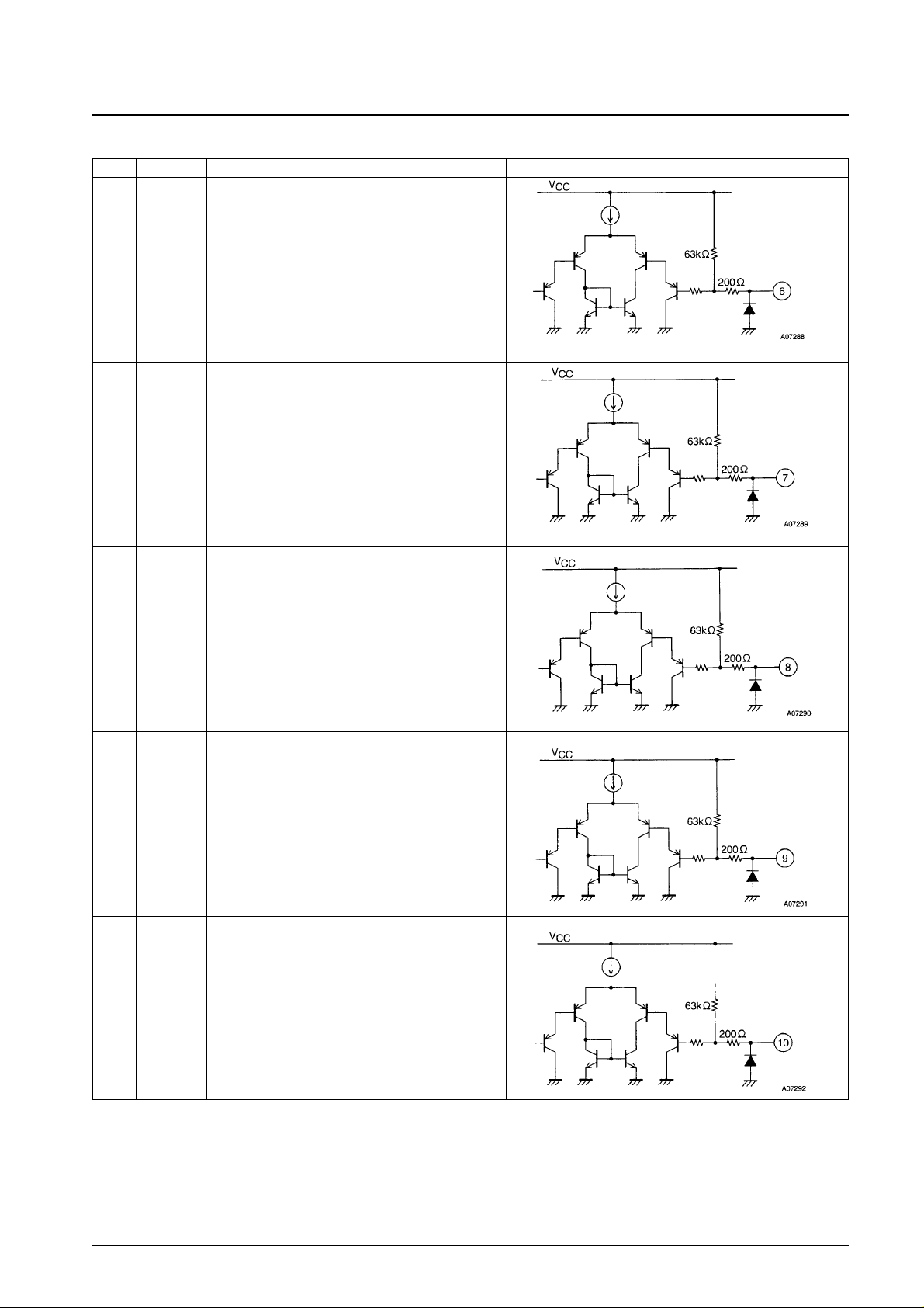
Pin No. Pin Functions Equivalent circuit
6 BR
Brake control (short braking operation)
Low: 0 to 1.5 V
High: 4.0 V to V
CC
An open state functions as a high-level input.
Low for start, high or open for brake mode operation.
The hysteresis is about 0.45 V.
7 F/R
Forward/reverse control
Low: 0 to 1.5 V
High: 4.0 V to V
CC
An open state functions as a high-level input.
Low for forward, high or open for reverse rotation.
The hysteresis is about 0.45 V.
8 CLK
External clock signal input
Low: 0 to 1.5 V
High: 4.0 V to V
CC
An open state functions as a high-level input.
The hysteresis is about 0.45 V.
f = 10 kHz, maximum
9 S/S
Start/stop control
Low: 0 to 1.5 V
High: 4.0 V to V
REG
An open state functions as a high-level input.
Low for start, high or open for stop mode operation.
The hysteresis is about 0.45 V.
10 N1
Speed discriminator count switching
Low: 0 to 1.5 V
High: 4.0 V to V
CC
An open state functions as a high-level input.
The hysteresis is about 0.45 V.
Continued on next page.
Page 13
No. 5686-13/16
LB1821M
Continued from preceding page.
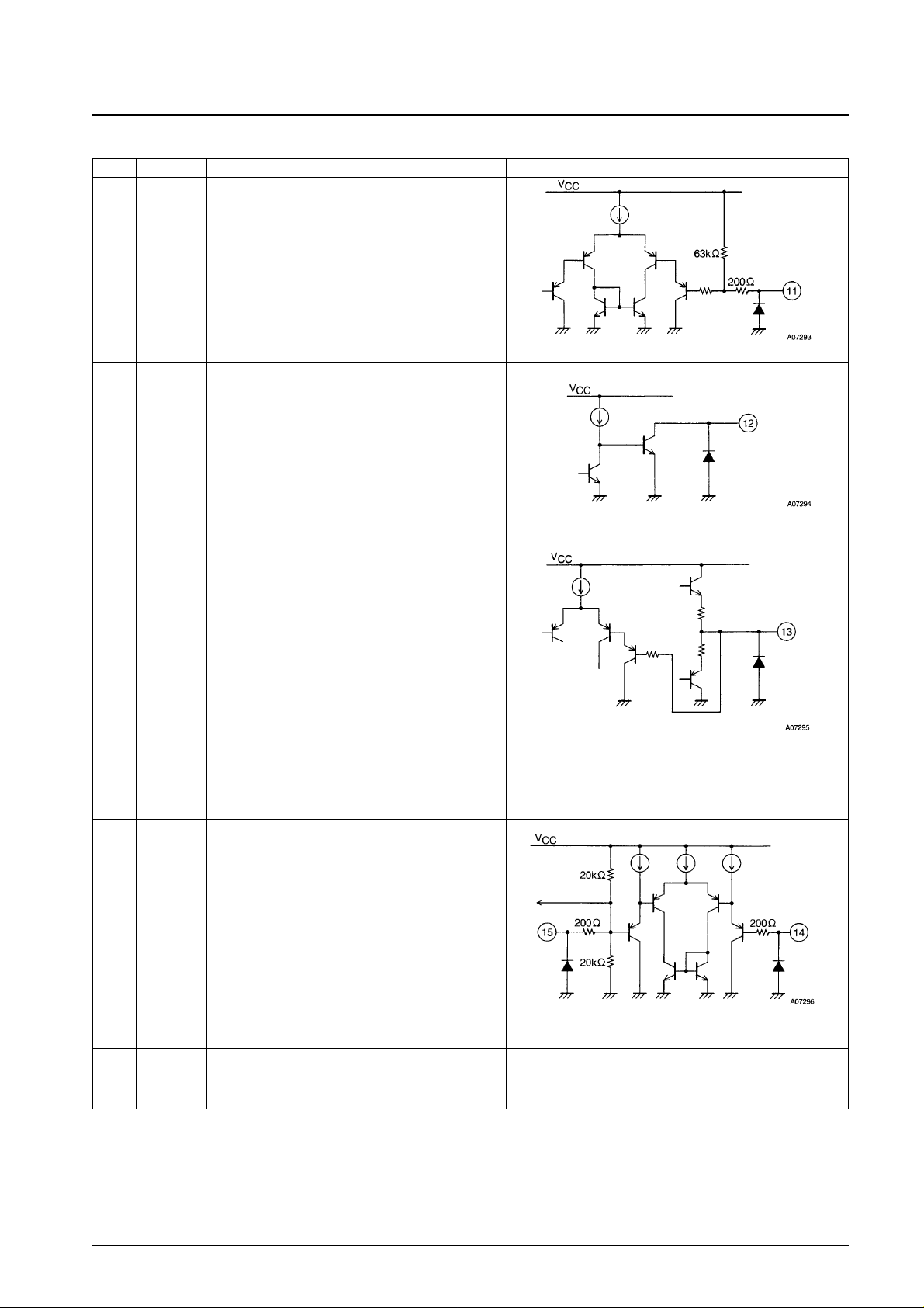
Pin No. Pin Functions Equivalent circuit
11 N2
Speed discriminator count switching
Low: 0 to 1.5 V
High: 4.0 V to V
CC
An open state functions as a high-level input.
The hysteresis is about 0.45 V.
12
FGS
OUT
FG amplifier output (after the Schmitt circuit)
This is an open collector output.
13
FG
OUT
FG amplifier output
This pin is connected to the FG Schmitt comparator circuit
internally in the IC.
14
FG
IN
–
FG amplifier inverting input
15
FG
IN
+
FG amplifier noninverting input (1/2 VCCpotential)
An initial reset is applied to the logic circuit block by
connecting an external capacitor (of about 0.1 µF) between
the FGIN+ pin and ground.
16 to 18
38 to 40
GND
Ground connections
These pins are all connected internally to the frame.
Continued on next page.
FG Schmitt comparator
FG reset circuit
Page 14
No. 5686-14/16
LB1821M
Continued from preceding page.
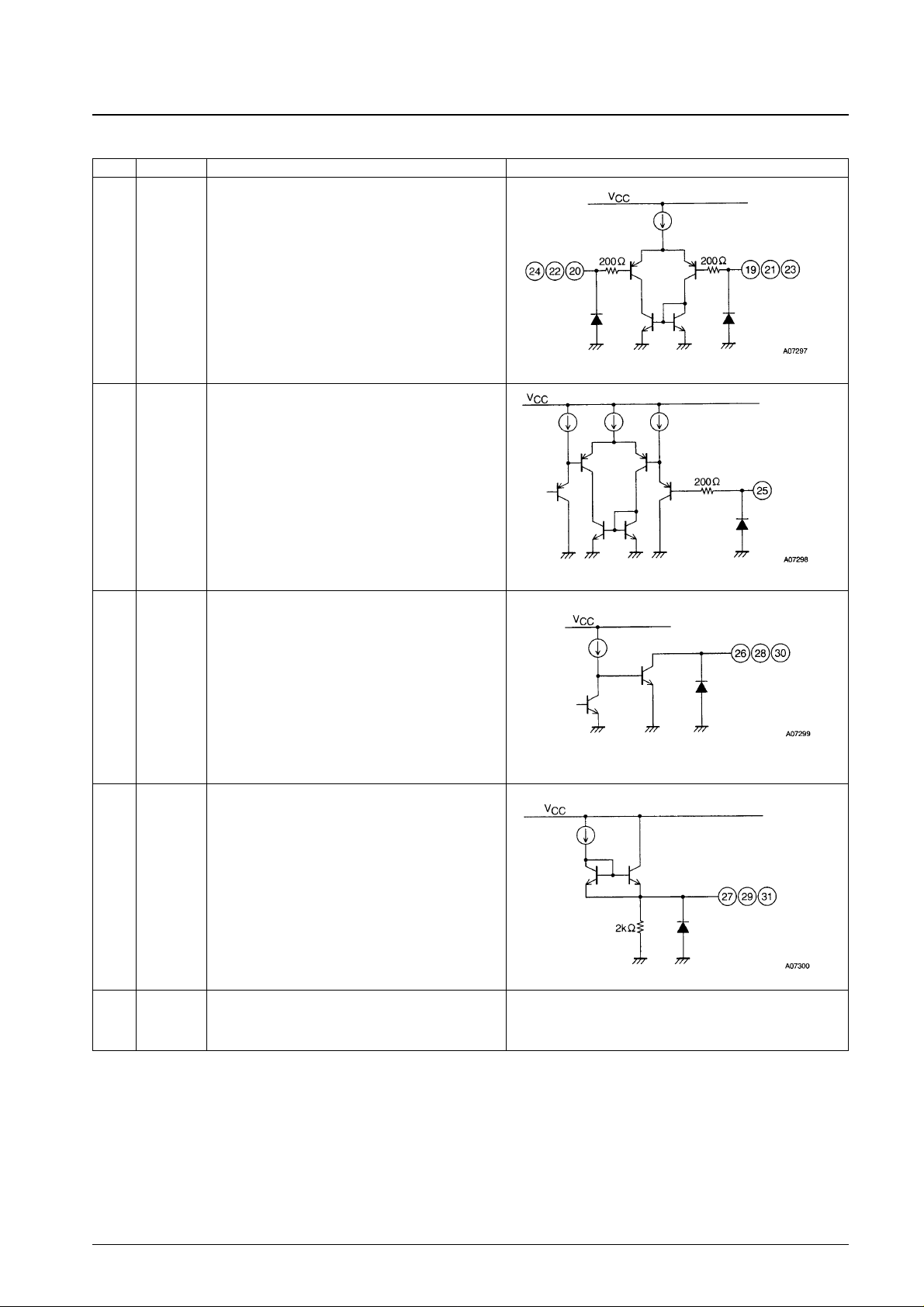
Pin No. Pin Functions Equivalent circuit
19
20
21
22
23
24
IN1
+
IN1
–
IN2
+
IN2
–
IN3
+
IN3
–
Hall inputs
High is defined as IN
+
> IN–, and low as the opposite.
An amplitude of 100 mV p-p (differential) or more is
desirable in the Hall signals. Connect capacitors between
the IN
+
and IN–pins if noise on the Hall signals causes
problems.
25 RF
Output current detection
Connect a resistor between this pin and ground.
The output limitation maximum current, I
OUT
, is set to be
0.52/R
f
by this resistor.
26
28
30
UL
VL
WL
This IC implements duty control using output signal PWM.
These are open collector sink outputs.
27
29
31
UH
VH
WH
Outputs (Fixed current source outputs)
32
V
CC
Power-supply voltage
Connect a capacitor between this pin and ground for power
supply stabilization.
Continued on next page.
Page 15
No. 5686-15/16
LB1821M
Continued from preceding page.
Pin No. Pin Functions Equivalent circuit
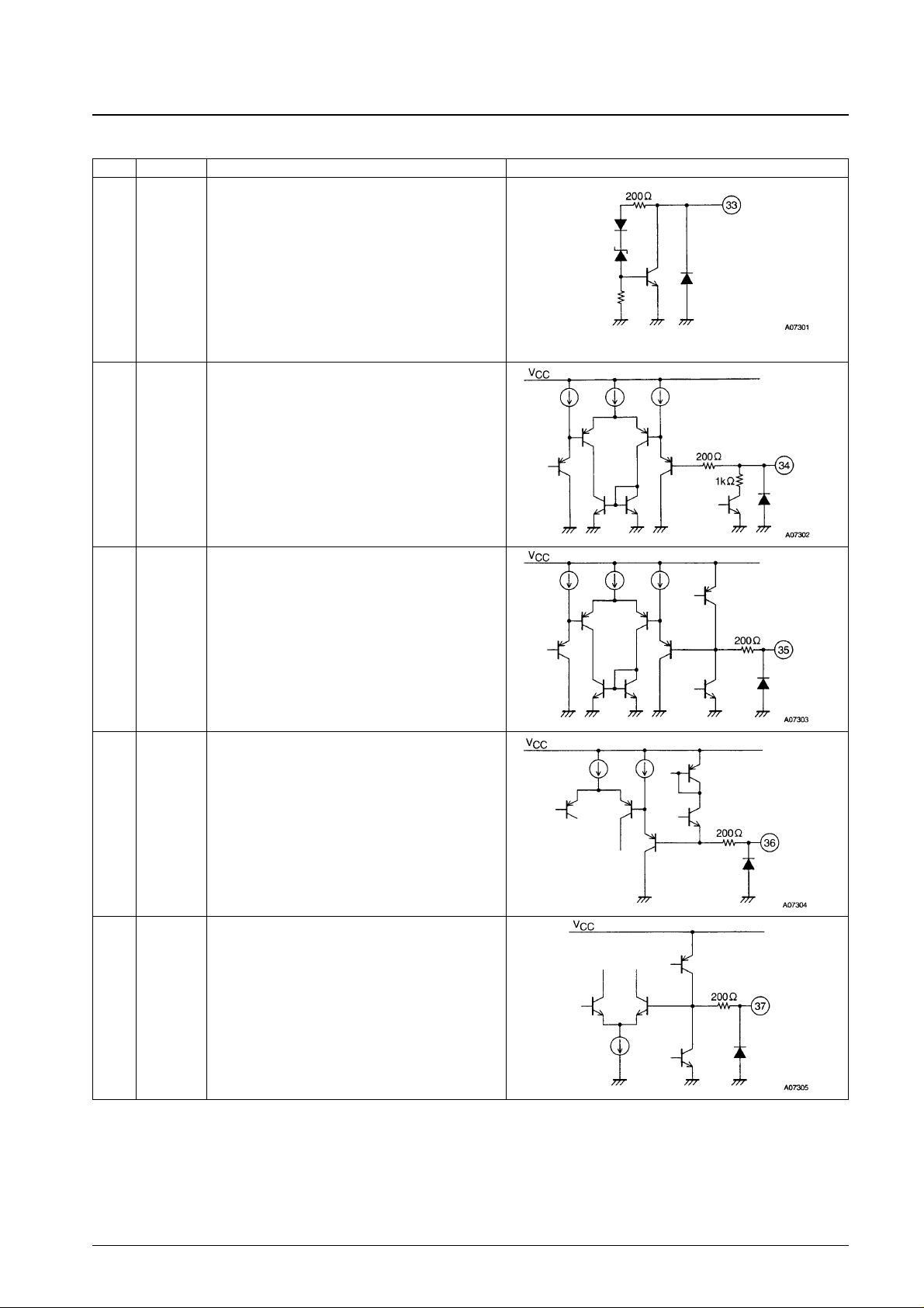
33
V
REG
7-V shunt regulator output
34 CR
PWM oscillator frequency setting
35 CROCK
Reference signal oscillator connection. This oscillator is
used by the motor constraint detection circuit, the clock
disconnection protection circuit, and other circuits.
A protection operation time of about 2.1 seconds can be set
up by connecting a capacitor of about 0.047 µF between
this pin and ground.
36 R
Setting for the charge current used for the VCO circuit C pin
Connect a resistor between this pin and ground. The value
of that resistor must not be lower than 2.7 kΩ.
37 C
VCO oscillator connection. This pin sets the VCO
frequency.
Connect a capacitor between this pin and ground.
Set the value of the capacitor so that the oscillator
frequency does not exceed 1 MHz.
Continued on next page.
Page 16
No. 5686-16/16
LB1821M
This catalog provides information as of June, 1997. Specifications and information herein are subject to change
without notice.
■ No products described or contained herein are intended for use in surgical implants, life-support systems, aerospace
equipment, nuclear power control systems, vehicles, disaster/crime-prevention equipment and the like, the failure of
which may directly or indirectly cause injury, death or property loss.
■ Anyone purchasing any products described or contained herein for an above-mentioned use shall:
➀ Accept full responsibility and indemnify and defend SANYO ELECTRIC CO., LTD., its affiliates, subsidiaries and
distributors and all their officers and employees, jointly and severally, against any and all claims and litigation and all
damages, cost and expenses associated with such use:
➁ Not impose any responsibility for any fault or negligence which may be cited in any such claim or litigation on
SANYO ELECTRIC CO., LTD., its affiliates, subsidiaries and distributors or any of their officers and employees
jointly or severally.
■ Information (including circuit diagrams and circuit parameters) herein is for example only; it is not guaranteed for
volume production. SANYO believes information herein is accurate and reliable, but no guarantees are made or implied
regarding its use or any infringements of intellectual property rights or other rights of third parties.
Continued from preceding page.
Pin No. Pin Functions Equivalent circuit
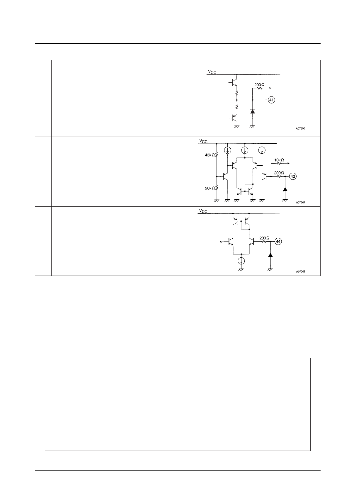
41
FIL
O
VCO filter amplifier output
This pin is connected to the VCO circuit internally in the IC.
42
FIL
I
VCO filter amplifier inverting input
This pin is connected through a 10-kΩ resistor internally in
the IC to the VCO system PLL output.
44 TOC
Torque command input
This pin is normally connected to the INT
.OUT
pin.
When the TOC voltage falls, the UL, VL, and WL PWM
duties are increased.
Do not apply a voltage in excess of V
CC
- 0.5 V. (An input
from a normal operational amplifier is desirable.)
VCO
input
CR
oscillation
signals
VCO PLL
output
 Loading...