

Page 1

Ordering number : EN6002
6.2
36
1
0.8
17.9
2.7
0.3
(4.9)
1.3
10.5
0.65
0.25
0.55
7.9
2.25
2.5max
0.1
LB1875
Monolithic Digital IC
LB1875
Polygon Mirror Motor Predriver IC
Overview
The LB1875 is a predriver IC for polygon mirror
motors. By using a driver array or discrete transistors (FETs) at the output, motor drive with high
rotation precision is possible. PAM drive or direct
PWM drive can be selected for the output to realize
high-efficiency control with minimum power loss.
Features
• Three-phase bipolar drive
• Direct PWM drive (bottom side) or PAM drive selectable
• PLL speed control circuit
• PWM oscillator
• Quartz oscillator
• Frequency divider
• FG with Schmitt comparator
• FG input single edge, dual edge selector circuit
• Integrating amplifier
• Phase lock detector output
• Current limiter
• Motor lock protection
• Thermal protection
• Forward/reverse circuit
• 5V regulator output
Package Dimensions
unit: mm
3235-HSOP36
[LB1875]
SANYO : HSOP36
Any and all SANYO products described or contained herein do not have specifications that can handle
applications that require extremely high levels of reliability, such as life-support systems, aircraft's
control systems, or other applications whose failure can be reasonably expected to result in serious
physical and/or material damage. Consult with your SANYO representative nearest you before using
any SANYO products described or contained herein in such applications.
SANYO assumes no responsibility for equipment failures that result from using products at values that
exceed, even momentarily, rated values (such as maximum ratings, operating condition ranges, or other
parameters) listed in products specifications of any and all SANYO products described or contained
herein.
SANYO Electric Co., Ltd. Semiconductor Business Headquarters
TOKYO OFFICE Tokyo Bldg., 1-10, 1 Chome, Ueno, Taito-ku, TOKYO, 110-8534 JAPAN
D0898RM(KI)
No. 6002-1/17
Page 2
LB1875
Specifications
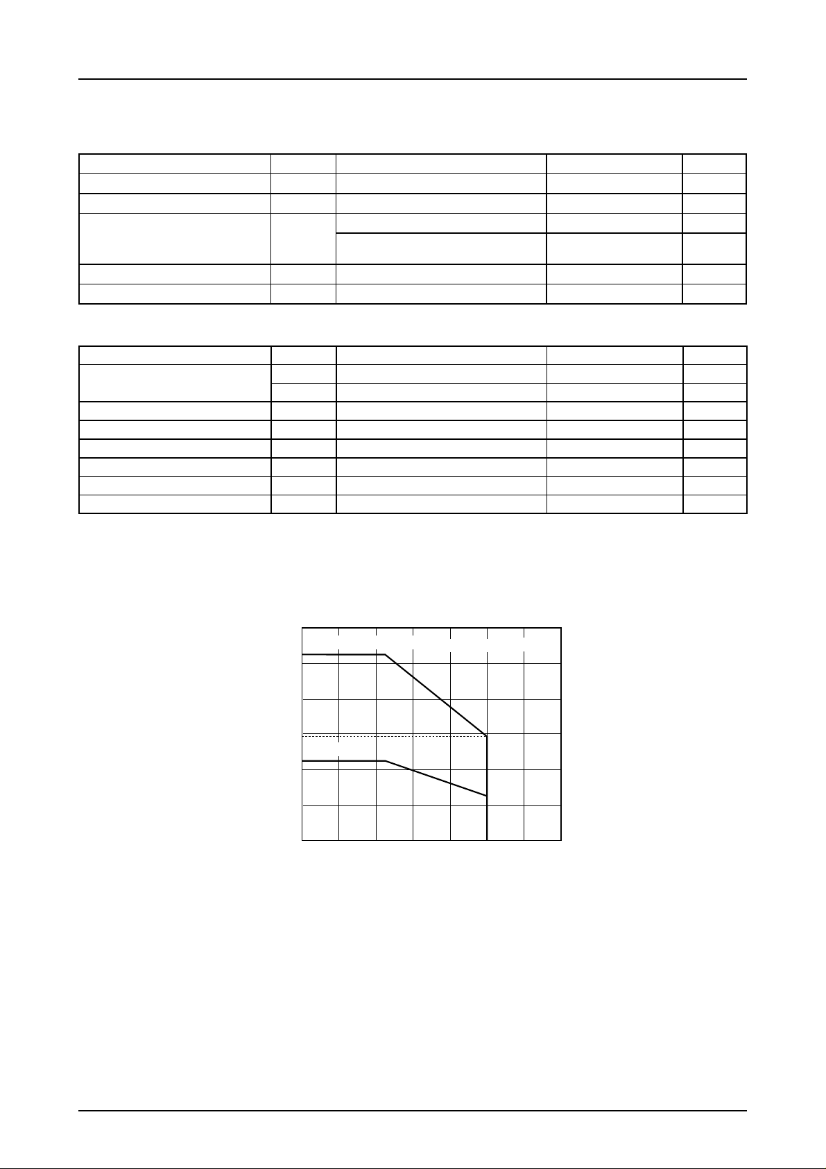
Maximum Ratings at Ta = 25°C
Parameter Symbol Conditions Ratings Unit
Maximum supply voltage V
Output current I
Allowable power dissipation Pd max IC only 0.9 W
Operating temperature Topr °C
Storage temperature Tstg °C
Operation Conditions at Ta = 25°C
Parameter Symbol Conditions Ratings Unit
Maximum supply voltage V
Output current I
5V regulated output current I
Voltage applied at LD pin V
LD pin output current I
Voltage applied at PWM pin V
PWM pin output current I
max 14.5 V
CC
max 30 mA
O
with substrate (114.3 x 76.1 x 1.6 mm3,
glass exposy)
2.1 W
– 20 to +80
– 55 to +150
1 8 to 13.5 V
CC
V
2
When shorted between V
CC
O
REG
LD
LD
PWM
PWM
CC
and V
REG
4.5 to 5.5 V
20 mA
0 to –20 mA
0 to 13.5 V
0 to 10 mA
0 to 13.5 V
0 to 20 mA
2.4
With substrate
2.1
2.0
1.6
1.2
Pd max – Ta
(114.3 x 76.1 x 1.6 mm, glass exposy)
IC only
0.9
0.8
0.4
Power dissipation, Pd max – W
0
0–20 20 40 60 80 100 120
Ambient temperature, Ta – ˚C
1.18
0.5
No. 6002-2/17
Page 3
LB1875
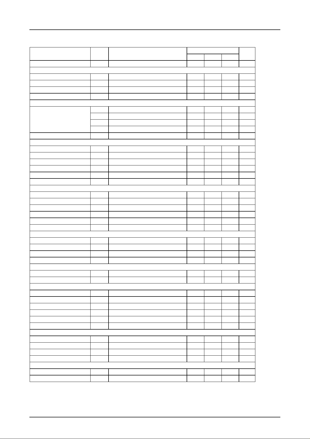
Electrical Characteristics at Ta = 25°C, VCC = 12V
Parameter
Power supply current I
Symbol Conditions
CC
[5V regulated output ]
Output fluctuation V
Voltage fluctuation ∆V
Load fluctuation ∆V
Temperature coefficcient ∆V
REG
1VCC=8 to 13.5V 40 100
REG
2IO=0 to –15 mA 20 100
REG
3 Design target value 0
REG
[Output Section]
Output saturation voltage V
(sat)1-1 UH, VH, WH "L" level, IO=50 µA 0.1 0.3 V
O
Vo(sat)1-2 UH, V H, WH " L" lev el, IO=10 mA 0.9 1.1 V
(sat)2 UH, VH, W H "L" leve l, IO=20 mA VCC–0.9 VCC–1.1 V
V
O
V
(sat)3 UL, VL, WL, IO=20 mA 0.2 0.4 V
O
Output leak current I
leak UL, VL, WL 10 µA
O
[Hall amplifier]
Input bias current I
Same-phase input voltage range V
(HA) –4 –1 µA
HB
ICM
Hall input sensitivity 30 mV
Hysteresis width ∆VIN(HA) 8 14 24 mV
Input voltage L->H V
Input voltage H->L V
SLH
SHL
[FG/Schmitt comparator section]
Input bias current I
Same-phase input voltage range V
Input sensitivity V
(FGS) –4 –1 µA
B
(FGS) 0 VCC–2.0 V
ICM
(FGS) 30 mV
IN
Hysteresis width ∆VIN(FGS) Design target value 8 14 24 mV
Input voltage L->H V
Input voltage H->L V
(FGS) Design target value 7 mV
SLH
(FGS) Design target value –7 mV
SHL
[PWM oscillator]
Output High level voltage V
(OSC) 2.7 3.0 3.3 V
OH
Output Low level voltage VOL(OSC) 1.5 1.8 2.1 V
Oscillator frequency f(OSC) C=2200 pF 30 kHz
Amplitude V(OSC) 1.0 1.2 1.4 V
[PWM output]
Output saturation voltage V
(PWM) I
OL
Output leak current IL(PWM) VO=V
=15 mA 0.9 2.0 V
PWM
CC
[CSD oscillator ]
Output High level voltage V
(CSD) 2.5 2.8 3.1 V
OH
Output Low level voltage VOL(CSD) 0.55 0.85 1.15 V
External C charge current I
External C discharge current I
Oscillator frequency f
Amplitude V
1 –13 –10 –7 µA
CHG
2 7 10 13 µA
CHG
C=0.068 µF 35 Hz
CSD
CSD
[Phase comparator output]
Output High level voltage V
Output Low level voltage V
Output source current I
Output sink current I
PD
PD
=–100 µAV
PDHIOH
=100 µA 0.1 0.2 V
PDLIOH
+
VPD=V
/2 –0.6 mA
–
REG
VPD=V
/2 1.5 mA
REG
[Phase lock detector output]
Output saturation voltage V
Output leak current IL(LD) VO=V
(LD) ILD=10 mA 0.1 0.4 V
OL
CC
Ratings
min typ max
30 40
4.65 5.0 5.35
0 VCC–2.0 V
7 mV
–7 mV
10 µA
1.75 1.95 2.15 V
–0.2 V
REG
–0.1 V
REG
10 µA
Continued on next page
Unit
mV/°C
mA
V
mV
mV
P-P
P-P
P-P
P-P
No. 6002-3/17
Page 4
LB1875
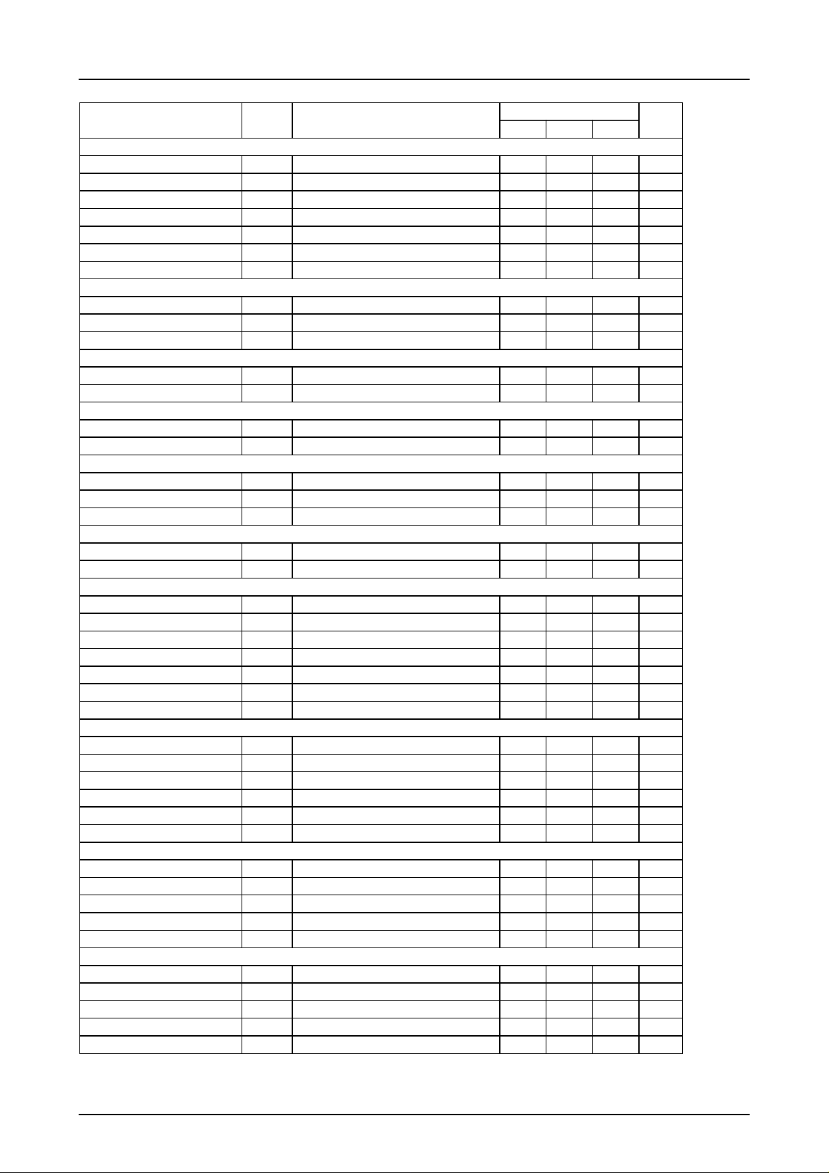
Continued from preceding page
Parameter Symbol Conditions
[ERR amplifier]
Input offset voltage V
(ER) Design target value –10 +10 mV
IO
Input bias current IB(ER) –1 +1 µA
Ouput High level voltage V
Ouput Low level voltage V
DC bias level V
(ER) IOH = –500 µAV
OH
(ER) IOL=500 µA 0.9 1.2 V
OL
(ER) –5% V
B
[Current limiter]
Limiter voltage V
RF
[Low-voltage protection circuit]
Operation voltage V
Release voltage V
SDL
SDH
Hysteresis width ∆VSD 0.15 0.25 0.35 °C
[Thermal shutdown operation]
Termal shutdown temperature TSD Design target value (junction temperature) 150 180 °C
Hysteresis width ∆TSD Design target value (junction temperature) 30 °C
[SOFT pin]
Stop voltage V
External C discharge current I
In stop condition 3.0 3.3 3.6 V
SFT
DCHG
[Quartz oscillator]
Quartz oscillator frequency f
Low level pin voltage V
High level pin voltage V
pin]
[CLK
OUT
Output saturation voltage
Output leak current IL(CKOUT) VO=V
pin]
[CLK
IN
External input frequency f
High level input voltage V
Low level input voltage V
Input open voltage V
Hysteresis width V
High level input current I
Low level input current I
OSC
OSCLIOSC
OSCHVOSC=VOSCL
VOL(CKOUT)
I(CKIN)
IH(CKIN)
IL(CKIN
IO(CKIN)
IS(CKIN)
IH(CKIN)VCKIN=VREG
IL(CKIN)VCKIN
=–0.5 mA 1.45 V
+0.6V 0.5 mA
I
=2 mA 0.1 0.4 V
CKOUT
CC
) 0 1.5 V
V
=0V –200 –140 µA
[S/S pin]
High level input voltage V
(SS) 3.5 V
IH
Low level input voltage VIL(SS) 0 1.5 V
Input open voltage V
Hysteresis width V
High level input current I
Low level input current I
(SS) V
IO
(SS) 0.3 0.4 0.5 V
IS
(SS) VS/S=V
IH
(SS) VS/S=0V –200 –140 µA
IL
REG
[F/R pin]
High level input voltage V
(FR) 3.5 V
IH
Low level input voltage VIL(FR) 0 1.5 V
Input open voltage V
High level input current I
Low level input current I
pin]
[FG
SEL
High level input voltage
Low level input voltage
Input open voltage
High level input current
Low level input current
(FR) V
IO
(FR) VF/R=V
IH
(FR) VF/R=0V –200 –140 µA
IL
(FSEL) 3.5 V
V
IH
(FSEL) 0 1.5 V
V
IL
(FSEL) V
V
IO
(FSEL) V
I
IH
(FSEL) V
I
IL
REG
FSEL=VREG
=0V –200 –140 µA
FSEL
Ratings
min typ max
–1.2 V
REG
–0.9 V
REG
/2 V
REG
+ 5%
0.45 0.5 0.55 V
3.55 3.75 3.95 V
3.8 4.0 4.2 V
4 6 8 µA
2 10 MHz
10 µA
0.1 10 kHz
3.5 V
–0.5 V
REG
REG
REG
0.3 0.4 0.5 V
–10 0 +10 µA
REG
–0.5 V
REG
REG
–10 0 +10 µA
REG
–0.5 V
REG
REG
–10 0 +10 µA
REG
–0.5 V
REG
REG
–10 0 +10 µA
Continued on next page
Unit
V
V
V
V
V
V
V
V
No. 6002-4/17
Page 5
LB1875
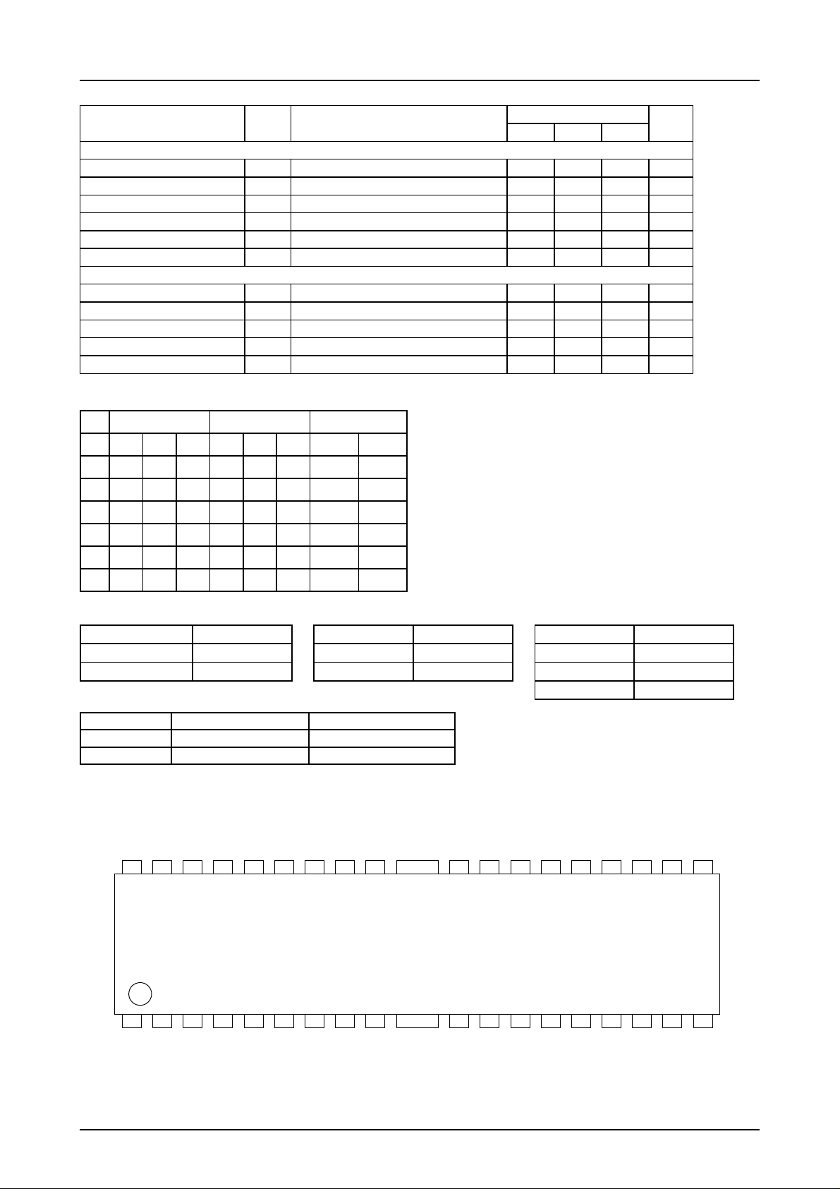
Continued from previous page
Parameter Symbol Conditions
[CLK
pin]
SEL
High level input voltage V
Middle level input voltage VIM(CSEL) 2.0 3.0 V
Low level input voltage V
Input open voltage V
High level input current I
Low level input current I
[LIM pin]
High level input voltage V
Low level input voltage VIL(LIM) 0 1.5 V
Input open voltage V
High level input current I
Low level input current I
(CSEL) 4.0 V
IH
(CSEL) 0 1.0 V
IL
(CSEL) V
IO
(CSEL) V
IH
(CSEL) V
IL
IH
IL
CSEL=VREG
=0V –200 –140 µA
CSEL
(LIM) 3.5 V
IH
(LIM) V
IO
(LIM) V
LIM=VREG
(LIM) V
=0V –200 –140 µA
LIM
3-phase logic truth table (IN = “H” indicates the IN+ > IN– condition)
Ratings
min t yp max
REG
–0.5 V
REG
–10 0 +10 µA
–0.5 V
REG
–10 0 +10 µA
REG
REG
REG
Unit
V
V
V
V
F/R= "L" F/R= "H"
IN1 IN2 IN3 IN1 IN2 IN3 SOURCE SYNC
1HLHLHL VH UL
2HLLLHHWH UL
3HHLLLHWH VL
4LHLHLH UH VL
5LHHHLL UH WL
6LLHHHL VH WL
Output
FGSEL pin
CLKSEL pinS/S pin
Input state Condition Input state Edge detection Input state Divisor
High or open Stop High or open FG dual edge High or open 1024 x 4
L Start L FG single edge M 1024
L 1024 x 3
LIM pin
Input state Output pin (UH, VH, WH) PWMOUT pin
High or open No PWM (PAM operation) PWM output
L PWM (direct PWN operation) FG/Schmitt comparator output
Pin Assignment
–
36
CSD
35
+
IN
IN
FG
FG
34
33
+
IN1
–
IN1
32
31
+
IN2
–
IN2
30
29
+
IN3
28
–
IN3
GND
27
V
CC
26
UL
25
UH
24
VL
23
VH
22
WL
21
WH
20
RF
OUT
PWM
19
1
REG
V
LB1875
2
3
4
5
6
7
8
F/R
9
SEL
FG
I
O
X
X
S/S
SEL
CLK
IN
CLK
OUT
CLK
GND
10
LIM
11
LD112LD2
13PD14
15
16
17
SOFT
18
PWM
C
A11348
I
O
E
E
TOC
No. 6002-5/17
Page 6

LB1875
Block Diagram and Sample Application Circuit
(Sample application: PAM drive, FET output)
V
REG
PDLD1LD2
V
REG
FG
IN
FG
IN
FGSEL
CLK
CLK
OUT
CLKSEL
CPWM
S/S
F/R
CSD
XO
–
+
IN
XI
CLK
OSC
PWM
OSC
S/S
F/R
SD
OSC
–
+
–
+
CLK
SELECT
ECL
1/8
LOGIC
FILTER
SELECT
PLL
1/128
1/384
1/512
FG
FG
HALL LOGIC
LD
LVSD TSD
V
REG
COMP
–
+
V
REG
PRI
DRIVER
PWM
EI
EO
TOC
PWM
OUT
V
CC
V
REG
UL
UH
VL
VH
WL
WH
12V
+
24V
+
+
HALL
HYS AMP
IN1+IN1–IN2+IN2–IN3+IN3–SOFT GNDLIM
V
CC
CURR
LIM
RF
A11596
Note: For applications where the motor has variable speed and control at low motor voltages is required, the base voltage of the
output interface transistor must be made low. In this case, a P-channel FET which can be used at low gate voltages must be
selected.
No. 6002-6/17
Page 7
LB1875
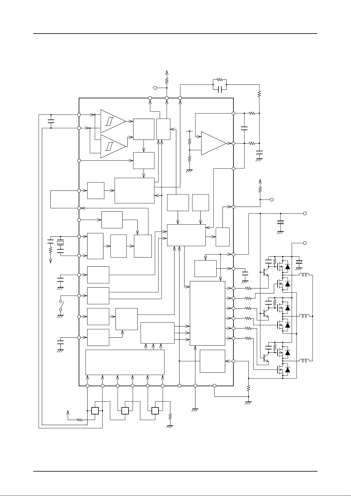
(Sample application: direct PWM drive, FET output)
V
REG
PDLD1LD2
V
REG
FG
IN
FG
IN
FGSEL
CLK
CLK
OUT
CLKSEL
XO
CPWM
–
–
+
+
–
+
IN
XI
CLK
OSC
PWM
OSC
CLK
SELECT
ECL
1/8
FILTER
SELECT
PLL
1/128
1/384
1/512
FG
FG
LD
V
REG
LVSD TSD
COMP
V
–
+
PWM
REG
EI
EO
TOC
PWMOUT
V
CC
V
REG
V
REG
FGS
12V
+
24V
+
S/S
F/R
CSD
IN1+IN1–IN2+IN2–IN3+IN3
V
CC
S/S
F/R
SD
OSC
LOGIC
HALL
HYS AMP
HALL LOGIC
–
DRIVER
SOFT GNDLIM
PRI
CURR
LIM
UL
UH
VL
VH
WL
WH
RF
A11597
No. 6002-7/17
Page 8
LB1875
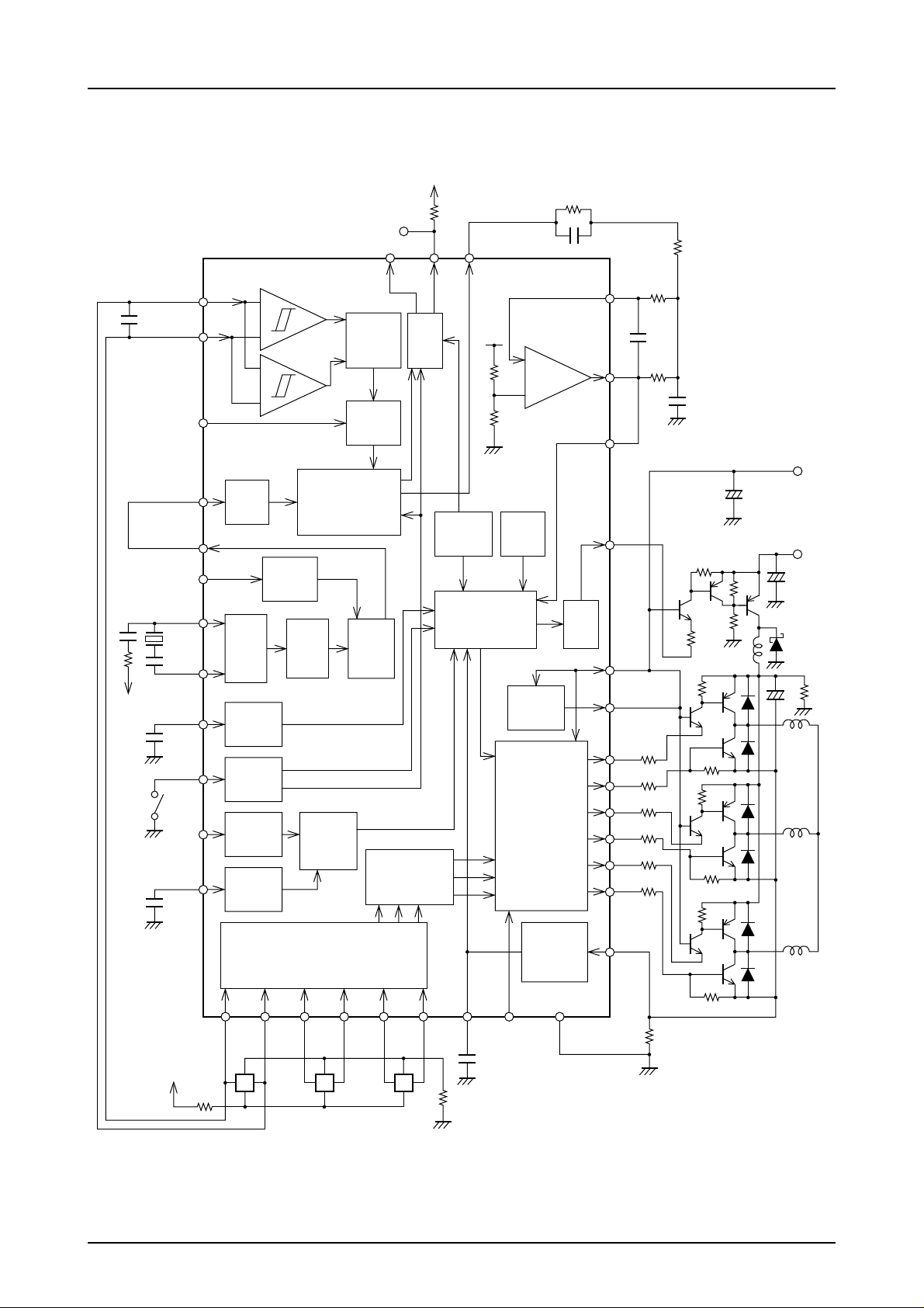
(Sample application: PAM drive, bipolar transistor output)
V
REG
PDLD1LD2
V
REG
FG
IN
FG
IN
FGSEL
CLK
CLK
OUT
CLKSEL
XO
CPWM
–
–
+
+
–
+
IN
XI
CLK
OSC
PWM
OSC
CLK
SELECT
ECL
1/8
FILTER
SELECT
PLL
1/128
1/384
1/512
FG
FG
LD
V
REG
LVSD TSD
COMP
V
–
+
PWM
REG
EI
EO
TOC
PWM
OUT
V
CC
V
REG
5V
+
24V
+
+
S/S
F/R
CSD
IN1+IN1–IN2+IN2–IN3+IN3–SOFT GNDLIM
V
CC
S/S
F/R
SD
OSC
LOGIC
HALL LOGIC
HALL
HYS AMP
PRI
DRIVER
CURR
LIM
UL
UH
VL
VH
WL
WH
RF
A11598
No. 6002-8/17
Page 9

LB1875
Description of the LB1875
1. Speed control circuit
This IC uses the PLL speed control technique which allows stable, high-precision motor rotation with low jitter. The PLL circuit
performs phase comparison of the falling edge of the clock input (CLKIN) with the edge of the FG input. Control is based on the
differential output.
When the FG
both edges are used, the FG waveform precision becomes critical.
When using an external clock input (supplied from CLKIN pin), the FG servo frequency is determined by the following equation.
fFG (servo) = f
fFG (servo) = f
When using the internal clock, the FG servo frequency is determined by the following equation. The number of FG pulses and the
quartz oscillator frequency determine the motor rotation speed.
fFG (servo) = f
fFG (servo) = f
f
: Quartz oscillator frequency
OSC
N: Clock divisor (see table)
2. Output drive
This IC allows selection of PAM drive or direct PWM drive.
When the LIM pin is Low , the direct PWM mode is selected. The ON duty cycle of the UH, VH, and WH output (external bottomside transistor drive output) changes, thereby controlling the motor speed. Current control is also realized by changing the ON duty
cycle to limit the current. At this time, the Schmitt comparator output of the FG is supplied at the PWM
transistors are used externally, the top-side transistors should not have an integrated diode, but Schottky barrier diodes should be used
instead (to prevent feedthrough current caused by diode reverse recovery during PWM switching).
When the LIM pin is High or open, the PAM drive mode is selected. The PWM
an external switching regulator circuit for varying the motor supply voltage and thereby controlling motor speed. Current control is
also realized by changing the motor supply voltage. In this case, a delay in the switching regulator circuit will cause a delay in the
current control action. During the delay, a higher current than the set current may flow, which must be taken into consideration when
selecting output transistors. For applications where the motor has variable speed and control at low motor voltages is required, the
lowest operation voltage is limited by the base voltage of the interface transistor for top-side output transistor drive. If this causes a
problem, the base voltage must be made low (for example by dividing the V
side output transistors, types which can be used at low gate voltages must be selected.
pin is Low , only the falling edge of the FG signal is valid. When the pin is High or open, both edges are valid. When
SEL
(FG
CLK
/2 (FG
CLK
/N (FG
OSC
/2N (FG
OSC
= Low)
SEL
= High or open)
SEL
= Low)
SEL
= High or open)
SEL
pin. When bipolar
OUT
pin carries the PWM signal. This output can drive
OUT
voltage with resistors). When FET s are used as top-
REG
3. Current limiting circuit
The current limiting circuit limits the peak current to the value I = VRF/Rf (VRF = 0.5V typ., Rf: current detector resistor). As
mentioned above, in PAM drive mode, a current higher than the set current may flow during the delay interval. If the capacitor
charge current of the switching regulator circuit is a problem, a smoothing capacitor may be inserted, with the negative side connected
to the RF pin.
If PWM noise is a problem in the RF waveform, a filter should be provided at the input.
No. 6002-9/17
Page 10
LB1875
4. Reference clock
Since the clock input of the PLL circuit (CLKIN) and the internal divisor output (CLK
possible.
(1) Using the internal divider circuit
Basically, CLKIN and CLK
are shorted. If a division ratio other than the built-in ratio is required, an external divider circuit can be
OUT
inserted between these two pins.
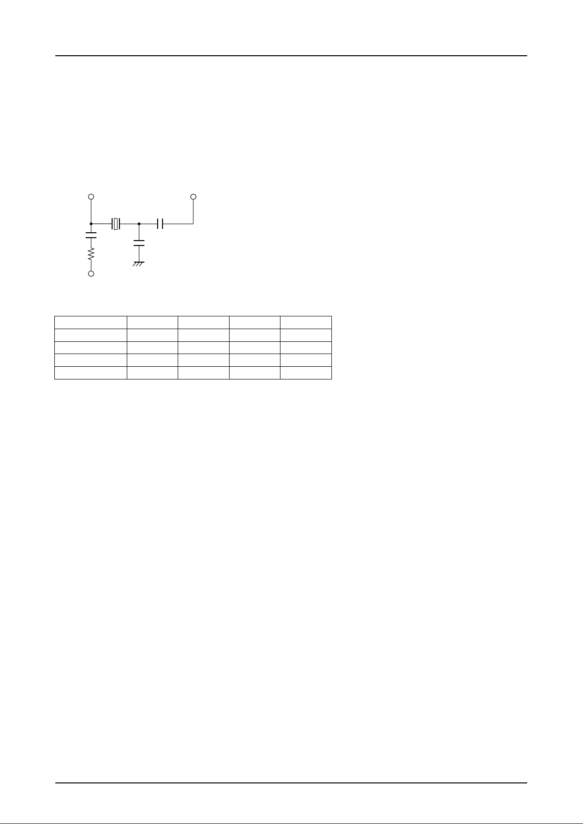
[1] Using a quartz oscillator
An oscillator using a quartz crystal and C, R components can be configured as shown below.
OUT
) are separate, various applications are
X
I
X
O
C1, R1 : For stable oscillation
V
C3
C1
C2
R1
REG
A11349
C2 : For overtone oscillation prevention
: For crystal coupling
C3
(Reference values)
Oscillator frequency (MHz) C1 (µF) C2 (pF) C3 (pF) R1 ( )
2 to 3 0.1 10 100 330k
3 to 7 0.1 None 47 330k
7 to 9 0.1 None 22 330k
9 to 10 0.1 None 12 330k
The circuit configuration and values are for reference only. The quartz crystal characteristics as well as the possibility of floating
capacitance and noise due to layout factors must be taken into consideration when designing an actual application.
[Precautions for wiring layout design]
Since the quartz oscillator circuit operates at high frequencies, it is susceptible to the influence of floating capacitance from the
circuit board. Wiring should be kept as short as possible and traces should be kept narrow.
[2] External clock input (equivalent to quartz oscillator, several MHz)
When using an external signal source instead of a quartz oscillator, a resistor of about 13 kΩ should be inserted in series at the X
input. The XO pin should be left open.
Signal input level
Low: 0 to 0.8 V
High: 2.5 to 5 V
(2) When not using the internal divider circuit
When using an external signal source to supply a signal equivalent to the FG frequency (several kHz), the signal is input via the
CLKIN pin. When not using a quartz oscillator, the X
pin should be left open or connected to the V
I
Ω
pin (XO is open).
REG
I
5. Hall input signal
The Hall input requires a signal with an amplitude of at least the hysteresis width (24 mV max.). Taking possible noise influences
into consideration, an amplitude of at least 100 mV is desirable. If noise at the Hall input is a problem, a noise-canceling capacitor
(about 0.001 to 0.1 µF) should be connected across the Hall input pins .
Since the same-phase input range is 0 to VCC–2V, a Hall element can be connected in series if 12V is applied at the VCC pin.
6. FG input signal
The FG input is designed mainly for input from a Hall element and has the same specifications as the Hall input. If the input is to be
used for an FG pattern or other very low-level signal, an external amplifier must be used to amplify the signal first.
When there is noise at the FG input, locking may be impaired and jitter may increase. If PWM switching noise or other noise is found
to be present, countermeasures such as making the Hall element power supply more stable or connecting a capacitor across the input
will be necessary.
No. 6002-10/17
Page 11

LB1875
7. PWM frequency
The PWM frequency is determined by the capacitance connected to the C
f PWM 1/(15000 x C)
.
=
.
The PWM frequency should be between 15 and 50 kHz. If the frequency is too low, noise and control performance may be a
problem. If it is too high, switching losses will increase.
8. LD output
The LD1 output is ON when phase lock is achieved. Phase lock is evaluated only by the phase (through edge comparison), not by
speed deviation. Therefore when LD1 is ON, speed deviation is affected by the FG signal acceleration for example when establishing
the lock condition. (The lower the acceleration, the lower the speed deviation.) When it is necessary to limit speed deviation when
LD1 is ON, the results of actual motor speed measurement must be applied.
9. Power supply
When using FETs as bottom-side output transistors, applying a voltage of 12V to the VCC pin makes it possible to supply a gate
voltage of about 10V. When using FETs or bipolar transistors that can handle a low gate voltage, the VCC and V
short- circuited to apply 5V. (In this case, do not apply voltage higher than 5.5V.)
Since this IC is designed for use in high-current motors, the power supply line may fluctuate easily. Therefore a capacitor of
sufficient capacitance must be provided between the VCC pin and ground, to assure stable operation. If a diode is used in the power
line for reverse-connection protection, power line fluctuations may be further increased, which will require more capacitance.
PWM
pin.
pins can also be
REG
10. Motor lock protection circuit
To protect the IC and the motor itself when rotation is inhibited, a motor lock protection circuit is provided. If the LD output is High
(unlocked) for a certain interval in the start condition, the external bottom-side transistors are turned off. The length of the interval
is determined by the capacitance at the CSD pin. A capacitance of 0.1 µF results in a trigger interval of about 10 seconds.
Trigger interval (S) 110 x C (µF)
.
=
.
The trigger interval should be set so as to leave sufficient leeway for motor startup. Speed reduction due to clock frequency switching
does not trigger the protection circuit.
When the protection circuit has been triggered, the condition can only be canceled by setting the system to the stop condition or by
turning the power off and on again. When wishing not to use the motor lock protection circuit, connect the CSD pin to ground.
11. Low voltage protection circuit
The low voltage protection circuit cuts off the bottom-side output transistors (external) when the voltage at the V
pin falls below
REG
3.75V (typ.). The circuit action is released when the voltage rises above approx. 4.0V (typ.).
12. F/R switching
Forward/reverse switching in principle should be carried out while the motor is stopped. If switching is carried out while the motor
is running, feedthrough current (due to output transistor delay) is prevented by the circuit design, but a high current will flow in the
output transistors (due to counterelectromotive voltage and coil resistance). If such a condition is anticipated, the output transistors
must be selected appropriately, to allow handling even higher current than in normal use.
13. Soft start
In PAM drive mode, connecting a capacitor (approx. 0.01 to 0.1 µF) between the SOFT pin and ground enables soft start (gradual
increase in PWM ON duty cycle, causing a sloped rise in motor supply voltage). This prevents the current flow exceeding the set
current due to switching regulator circuit delay at startup. The Soft start function is active only immediately after motor startup.
When the motor is stopped, the output transistors are turned off, therefore the charge accumulated in the switching regulator smoothing
capacitors can only be discharged as leak current of the output transistors. When the motor is restarted before the supply voltage has
dropped, the soft start function will not be active. Therefore it is necessary to discharge the capacitors via a resistor so that the soft
start function operates properly.
No. 6002-11/17
Page 12
LB1875
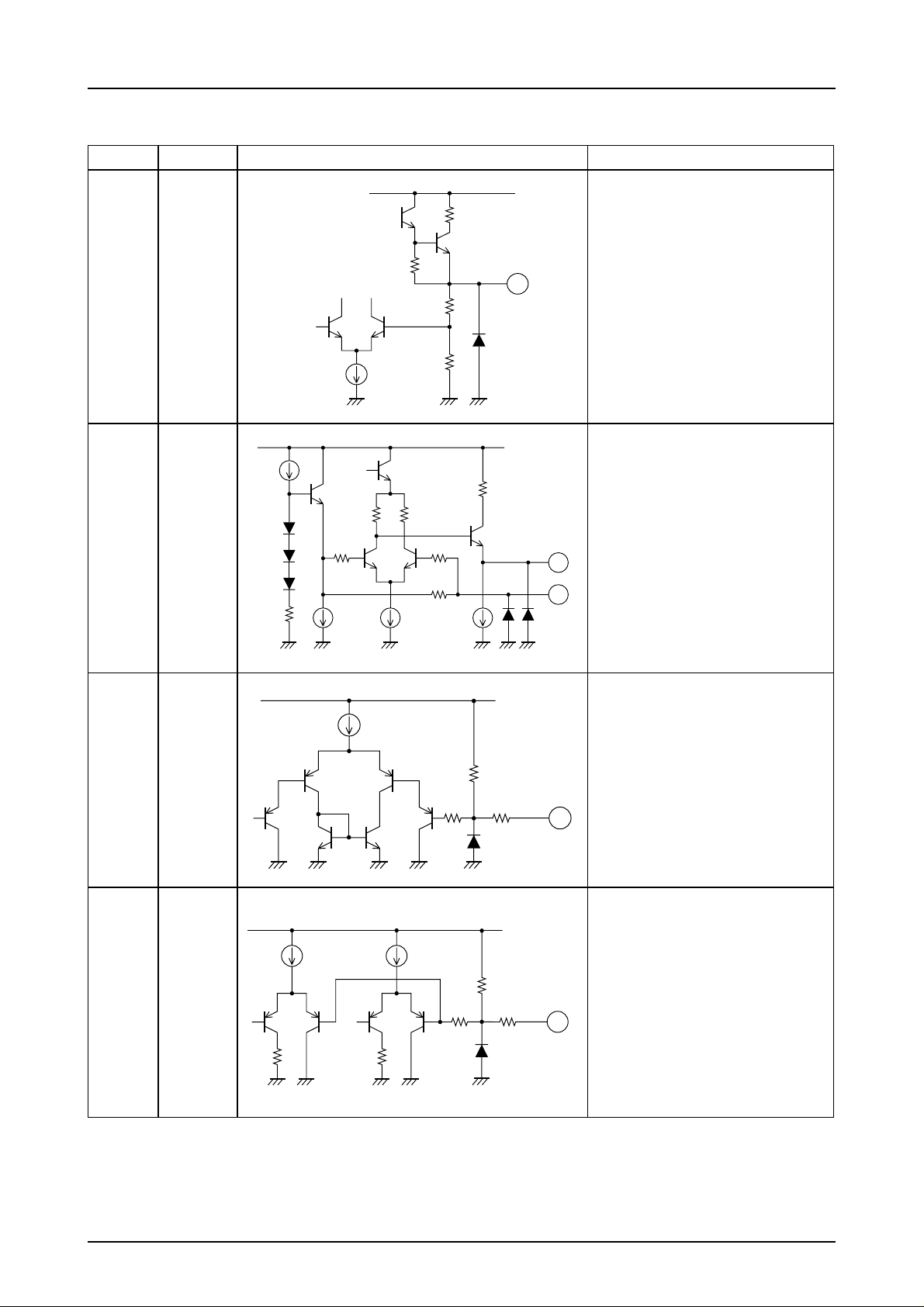
Pin Descriptions
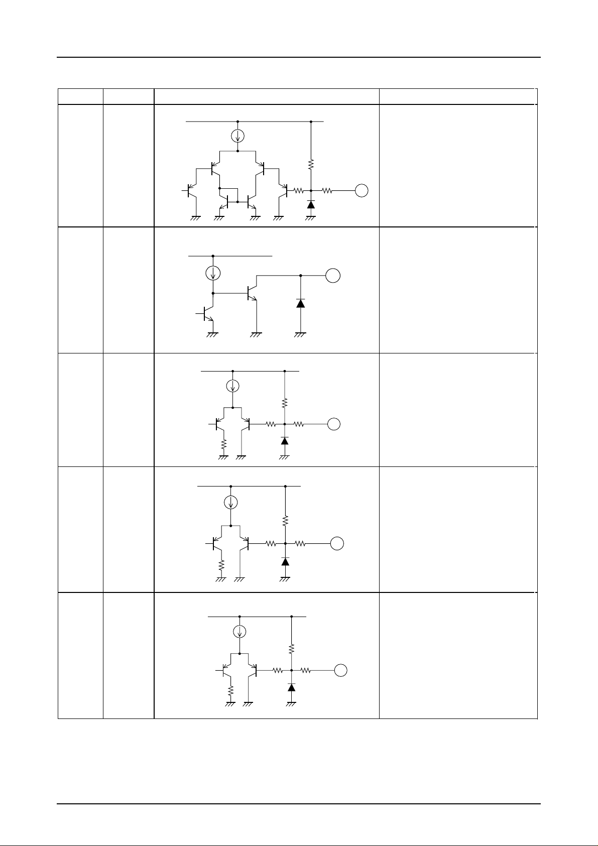
Pin number Pin n a me Equivalent circuit Pin function
1V
2X
3X
REG
V
CC
5V regulator output (control circuit
power supply)
For stable operation, pin should be
connected to ground via a capacitor
(0.1 µF or more).
1
A11350
I
O
V
REG
Pin 2: Quartz oscillator input. Maximum
oscillation frequency is 10 MHz
Pin 3: Quartz oscillator output
Generates reference clock. When an
external clock (several MHz) is used,
connect a resistor of about 13 k in
series to the X
3
input via the resistor. Leave the XO pin
2
open.
pin, so that the signal is
I
Ω
4 S/S
5 CLK
A11351
V
REG
Start/stop pin
Low: Start
High: Stop
High when open.
30 kΩ
5.6 KΩ
SEL
V
REG
4
A11352
Divisor selector pin
"L": (divisor 3072): 0 to 1.0V
"M": (divisor 1024): 2.0 to 3.0V
30 kΩ
5.6 kΩ
"H": (divisor 4093): 4.0V to V
High when open.
5
A11353
REG
Continued on next page
No. 6002-12/17
Page 13
LB1875
Continued from preceding page
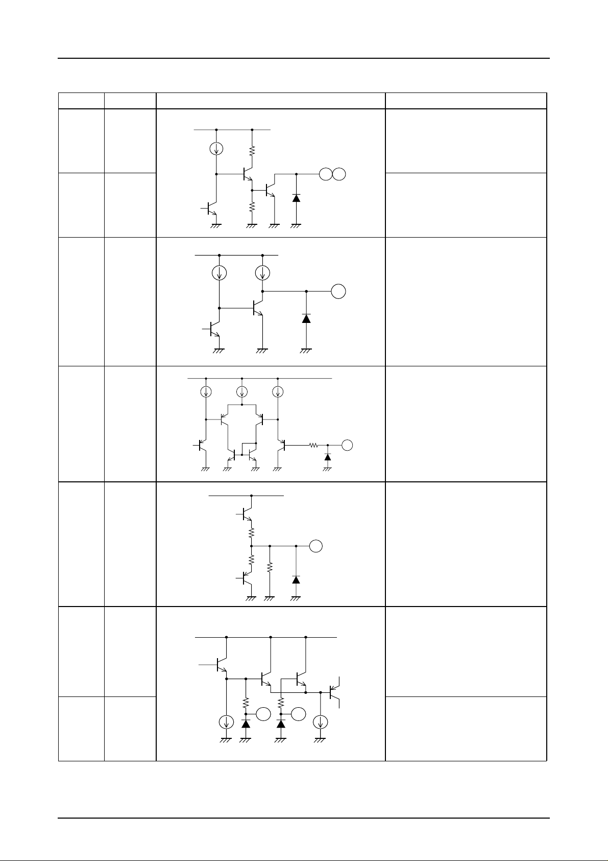
Pin number Pin name Equivalent circuit Pin function
6 CLK
IN
V
REG
Clock input (max. 10 kHz)
Low: 0 to 1.5V
High: 3.5V to V
REG
High when open.
30 kΩ
7 CLK
8 F/R
9FG
OUT
SEL
V
V
REG
V
REG
REG
30 kΩ
30 kΩ
5.6 kΩ
5.6 kΩ
5.6 KΩ
7
A11355
A11356
6
A11354
Quartz oscillator divider output
Ratio is selected with pin 5.
Open collector output
Forward/reverse switching pin
Low: 0 to 1.5V
High: 3.5V to V
REG
High when open.
8
FG comparator selector pin
Low: 0 to 1.5V
–> Speed control on FG single edge
High: 3.5V to V
9
–> Speed control on FG dual edge
High when open.
REG
10 LIM
V
REG
30 kΩ
5.6 kΩ
A11357
A11358
Drive mode selector pin
Low: 0 to 1.5V
–> Direct PWM drive mode
High: 3.5 V to V
REG
–> PAM drive mode
10
High when open.
Continued on next page
No. 6002-13/17
Page 14
LB1875
Continued from preceding page
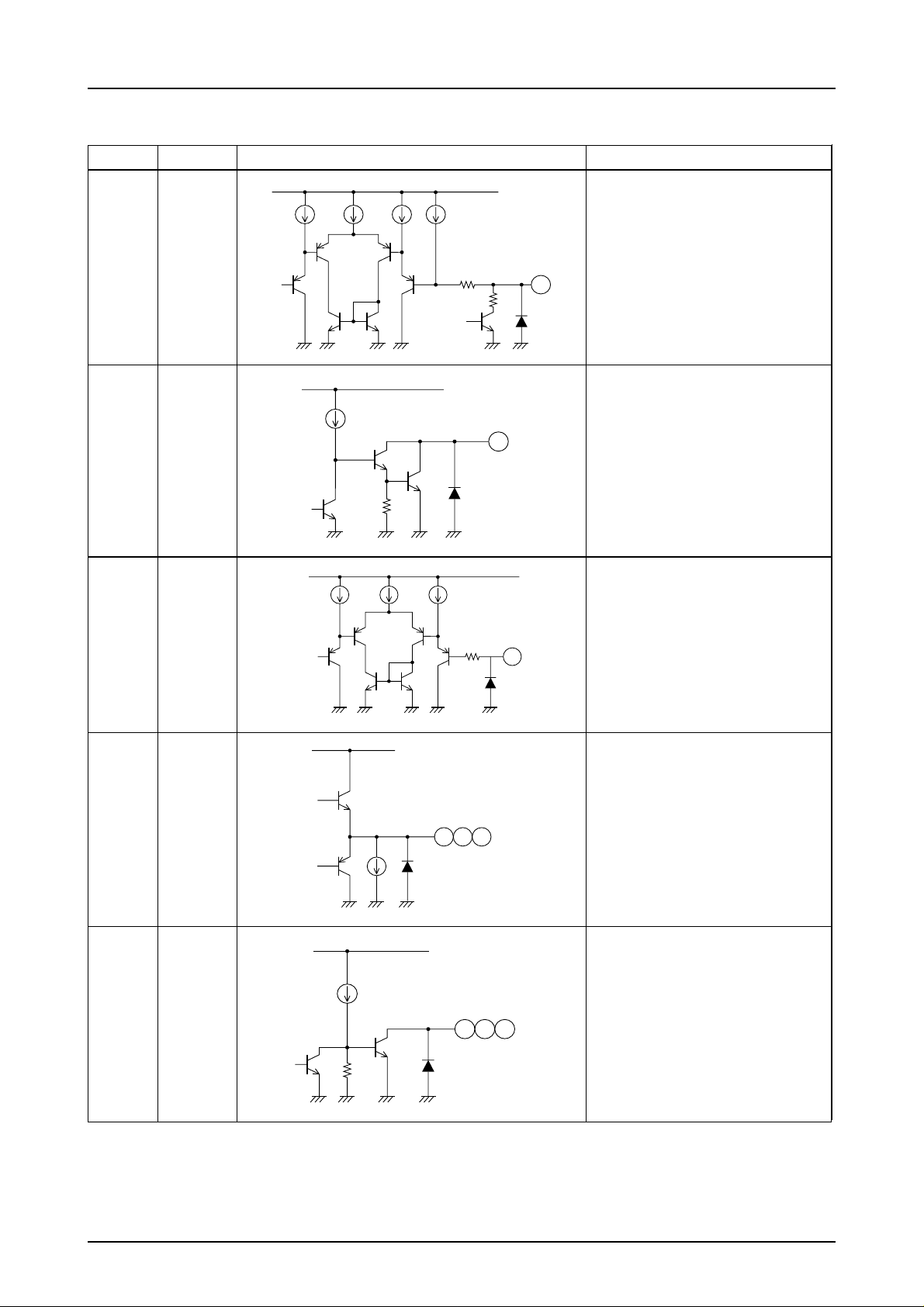
Pin number Pin name Equivalent circuit Pin function
11 LD1
I
V
REG
Phase lock detector output
On when PLL phase lock is achieved.
Open collector output
12 LD2
13 PD
14 E
11 12
Phase lock detector output
(LD1 inverted output)
On when PLL phase lock is achieved.
Open collector output
Phase comparator output (PLL output)
Outputs the phase difference as a signal
V
A11359
REG
with changing pulse duty cycle. The
13
higher the duty cycle, the higher the
output current.
A11360
I
V
REG
200Ω
14
Differential amplifier input
15 E
16 TOC
17 SOFT
O
V
REG
V
REG
200Ω
17
20 kΩ
200Ω
16
15
A11362
A11363
A11361
Differential amplifier output
Output current increases at Low.
Torque control input
Normally connected to EO pin. When
TOC pin goes Low, duty cycle of UH,
VH, WH (direct PWM mode) or PWM
output (PAM mode) changes, resulting
in increased torque.
Soft start control pin
Connect to ground via a capacitor.
Leave open when soft start is not to be
used.
Continued on next page
No. 6002-14/17
Page 15
LB1875
Continued from preceding page
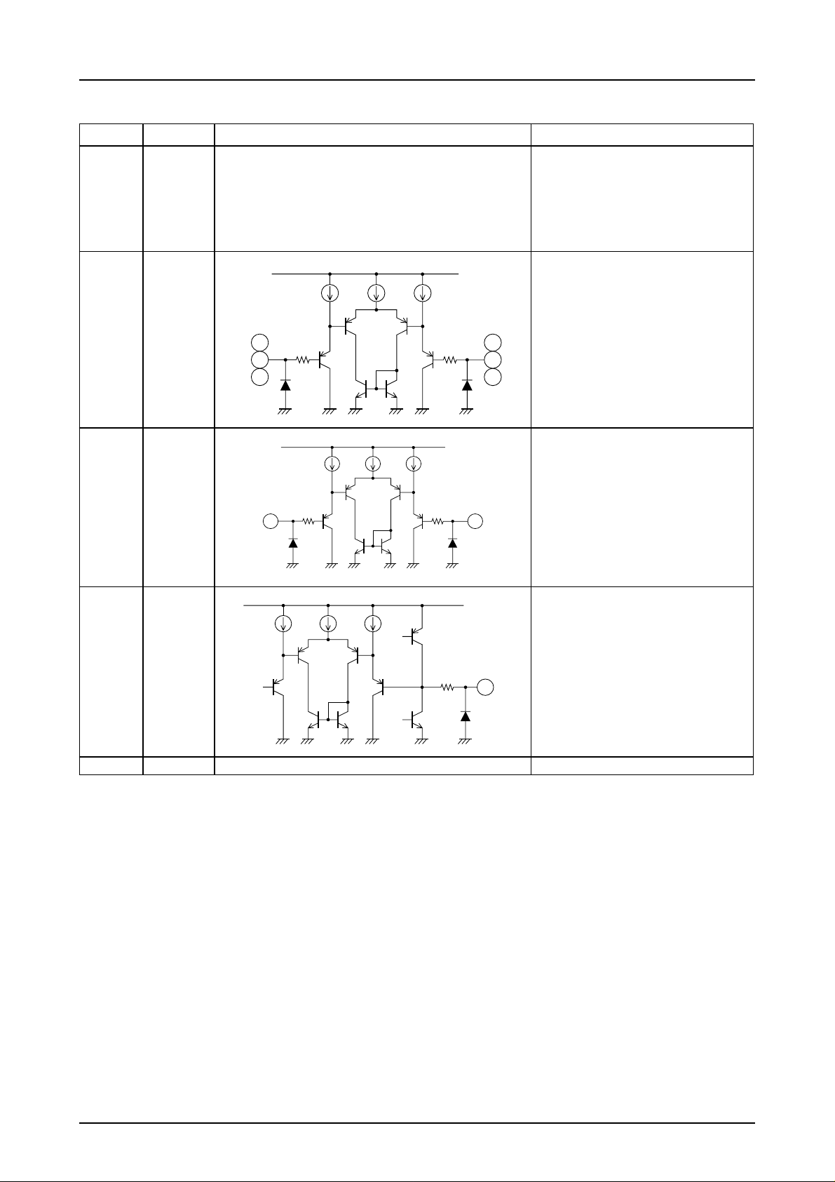
Pin number Pin name Equivalent circuit Pin function
18 PWM
V
REG
PWM oscillator pin
Connect to ground with a capacitor to
set oscillation frequency.
19 PWM
20 RF
21 WH
23 VH
25 UH
200Ω
2 kΩ
OUT
V
REG
18
A11364
PWM output
Open collector output (Darlington
connection). In direct PWM mode (LIM
19
pin Low) the output is an FG Schmitt
output.
A11365
V
REG
Output current detector pin
Connect to ground via a lower resistor.
Sets maximum output current I
OUT
=
0.5/Rf.
5 kΩ
23
A11366
V
CC
Output pin (for external bottom-side
transistor drive)
Performs duty cycle control in direct
PWM mode (LIM pin Low).
22 WL
24 VL
26 UL
21 23 25
A11367
V
CC
Output pin (for external bottom-side
transistor drive) .
Open collector output.
22 24 26
A11368
Continued on next page
No. 6002-15/17
Page 16
LB1875
Continued from preceding page
Pin number Pin na me Equivalent circuit Pin function
27 V
33 IN1
32 IN1
31 IN2
30 IN2
29 IN3
28 IN3
35 FG
34 FG
CC
Power supply pin (output and regulator
circuit power supply). Connect to
ground via capacitor to prevent noise.
When using the IC with a single 5V
source, short this pin to the V
+
–
+
–
+
–
+
IN
–
IN
V
CC
29
31
200Ω
33
V
CC
200Ω
28
30
32
A11369
Hall inputs for various phases
Logic "High" indicates V
FG comparator input
Pin 35: Non-inverted input
Pin 36: Inverted input
IN
REG
+
>VIN-.
pin.
36 CSD
FRAME GND
V
REG
35
200Ω
200Ω
34
A11370
Reference signal oscillator for motor
lock protection circuit, clock interruption error protection circuit etc.
Connect to ground via capacitor.
200Ω
19
A11371
Connect directly to ground if protection
circuit is not to be used.
Ground
No. 6002-16/17
Page 17

LB1875
Specifications of any and all SANYO products described or contained herein stipulate the performance,
characteristics, and functions of the described products in the independent state, and are not guarantees
of the performance, characteristics, and functions of the described products as mounted in the customer's
products or equipment. To verify symptoms and states that cannot be evaluated in an independent device,
the customer should always evaluate and test devices mounted in the customer's products or equipment.
SANYO Electric Co., Ltd. strives to supply high-quality high-reliability products. However, any and all
semiconductor products fail with some probability. It is possible that these probabilistic failures could
give rise to accidents or events that could endanger human lives, that could give rise to smoke or fire,
or that could cause damage to other property. When designing equipment, adopt safety measures so
that these kinds of accidents or events cannot occur. Such measures include but are not limited to protective
circuits and error prevention circuits for safe design, redundant design, and structural design.
In the event that any or all SANYO products(including technical data,services) described or
contained herein are controlled under any of applicable local export control laws and regulations,
such products must not be exported without obtaining the export license from the authorities
concerned in accordance with the above law.
No part of this publication may be reproduced or transmitted in any form or by any means, electronic or
mechanical, including photocopying and recording, or any information storage or retrieval system,
or otherwise, without the prior written permission of SANYO Electric Co. , Ltd.
Any and all information described or contained herein are subject to change without notice due to
product/technology improvement, etc. When designing equipment, refer to the "Delivery Specification"
for the SANYO product that you intend to use.
Information (including circuit diagrams and circuit parameters) herein is for example only ; it is not
guaranteed for volume production. SANYO believes information herein is accurate and reliable, but
no guarantees are made or implied regarding its use or any infringements of intellectual property rights
or other rights of third parties.
This catalog provides information as of December, 1998. Specifications and information herein are subject to change
without notice.
No. 6002-17/17
PS
 Loading...