

Page 1
Overview
The LB1825 is a three-phase brushless motor driver IC
optimal for LBP polygon mirror and magneto-optical disk
spindle motor drive.
Functions and Features
• Three-phase full-wave current control drive
• PLL speed control
• Internal 24-mode clock divisor switching
• Phase lock detector output
• FG/Hall FG selection
• Current limiter circuit
• 7 V stabilized power supply output pin
• Reverse torque braking
• Crystal oscillator circuit
• Internal/external reference frequency selection
• Built-in FG amplifier and FG pulse output
• Forward/reverse rotation switching
• Low power supply voltage protection circuit
• Thermal protection circuit
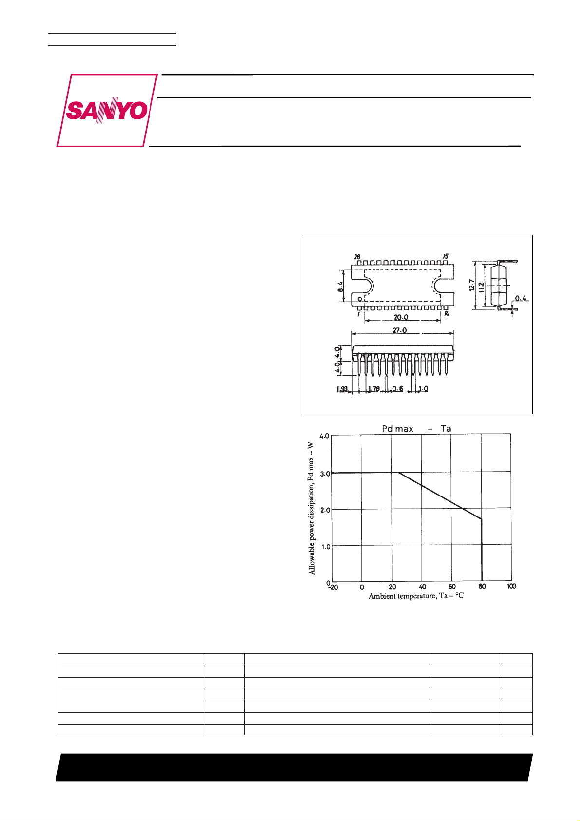
Package Dimensions
unit: mm
3147A-DIP28H
Monolithic Digital IC
Ordering number : EN4845B
83097HA (OT)/N3095HA (OT)/91494TH (OT) No. 4845-1/9
SANYO: DIP28H
[LB1825]
SANYO Electric Co.,Ltd. Semiconductor Bussiness Headquarters
TOKYO OFFICE Tokyo Bldg., 1-10, 1 Chome, Ueno, Taito-ku, TOKYO, 110 JAPAN
Three-Phase Brushless Motor Driver
LB1825
Specifications
Absolute Maximum Ratings at Ta = 25°C
Parameter Symbol Conditions Ratings Unit
Maximum supply voltage V
CC
max 30 V
Maximum output current I
O
max t < 0.1 s 2.0 A
Allowable power dissipation
Pd max1 Independent IC 3 W
Pd max2 With an arbitrarily large heat sink 20 W
Operating temperature Topr –20 to +80 °C
Storage temperature Tstg –55 to +150 °C
Page 2
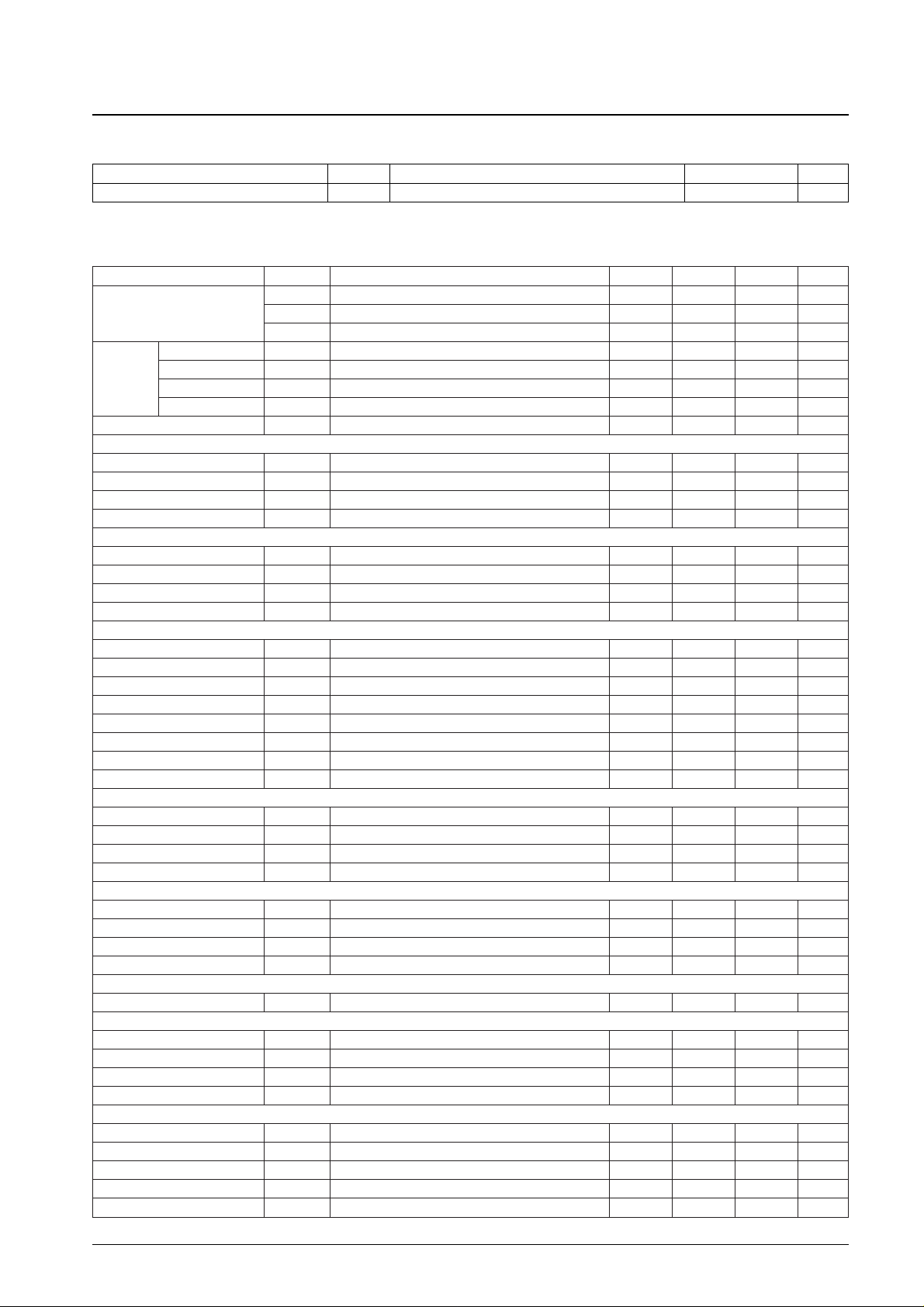
Allowable Operating Ranges at Ta = 25°C
Electrical Characteristics at Ta = 25°C, VCC= 24 V
No. 4845-2/9
LB1825
Parameter Symbol Conditions Ratings Unit
Supply voltage V
CC
10 to 28 V
Parameter Symbol Conditions min typ max Unit
I
CC
1 Braking stopped mode 35 47 mA
Current drain I
CC
2 FG
OUT
1 stopped mode 35 47 mA
I
CC
3 External clock, braking stopped mode 28 40 mA
Upper transistor (1) V
O
(sat)1 IO= 1.0 A 1.0 1.6 V
Upper transistor (2) V
O
(sat)2 IO= 1.5 A 1.25 2.1 V
Lower transistor (1) V
O
(sat)1 IO= 1.0 A 0.6 1.0 V
Lower transistor (2) V
O
(sat)2 IO= 1.5 A 0.9 1.6 V
Output leakage current I
O LEAK
100 µA
[Fixed voltage block]
Output voltage V
REGIREG
= 20 mA 6.3 7.0 7.8 V
Output current I
REG
20 mA
Load variation ∆V
REGIREG
= 0 to 20 mA 0.25 V
Temperature coefficient
αV
REG
Design target value –2.0 mV/°C
[Hall input block]
Input bias current I
B
(HA) 1 4 µA
Common-mode input range 1.5 V
CC
– 1.8 V
Input sensitivity DV
H
20 mV
Input offset voltage V
IOH
20 mV
[Drive block]
Dead zone width V
DZ
50 200 mV
Output idling voltage V
ID
6 mV
Forward gain G
DF
+
0.4 0.5 0.6
Reverse gain G
DF
–
–0.6 –0.5 –0.4
Accelerate command voltage V
STA
6.0 6.3 V
Decelerate command voltage V
STO
0.8 1.5 V
Forward limiter voltage V
L
+
Rf= 1.8 Ω 0.45 0.53 0.61 V
Reverse limiter voltage V
L
–
Rf= 1.8 Ω 0.45 0.53 0.61 V
[Phase comparator block]
Output high level voltage V
PDH
No external load V
REG
– 0.4 V
Output low level voltage V
PDL
No external load 0.4 V
Output source current I
PD
+
0.4 mA
Output sink current I
PD
–
2.5 mA
[Error amplifier block]
Input bias current I
B
(ER) 1 µA
Input offset voltage V
IO
(ER) –10 +10 mV
Output high level voltage V
ERH
No external load 5.5 V
Output low level voltage V
ERL
No external load 1.0 V
[Lock detector block]
Output saturation voltage V
LD
(sat) ILD= 10 mA 0.4 V
[FG amplifier block]
Input bias current I
B
(FG) 1 µA
Input offset voltage V
IO
(FG) –10 +10 mV
Output high level voltage V
FGH
No external load 5.0 V
Output low level voltage V
FGL
No external load 2.0 V
[FG Schmitt block]
Input operating level V
IS
FG
OUT
1 generation signal 160 mVp-p
Input hysteresis (high → low) V
SHL
External clock, braking stopped mode 0 mV
Input hysteresis (low → high) V
SLH
External clock, braking stopped mode 36 mV
Hysteresis V
FGS
18 36 60 mV
Output saturation voltage V
FG2
(sat) I
FG2
= 10 mA 0.4 V
Continued on next page.
Output
saturation
voltage
Page 3
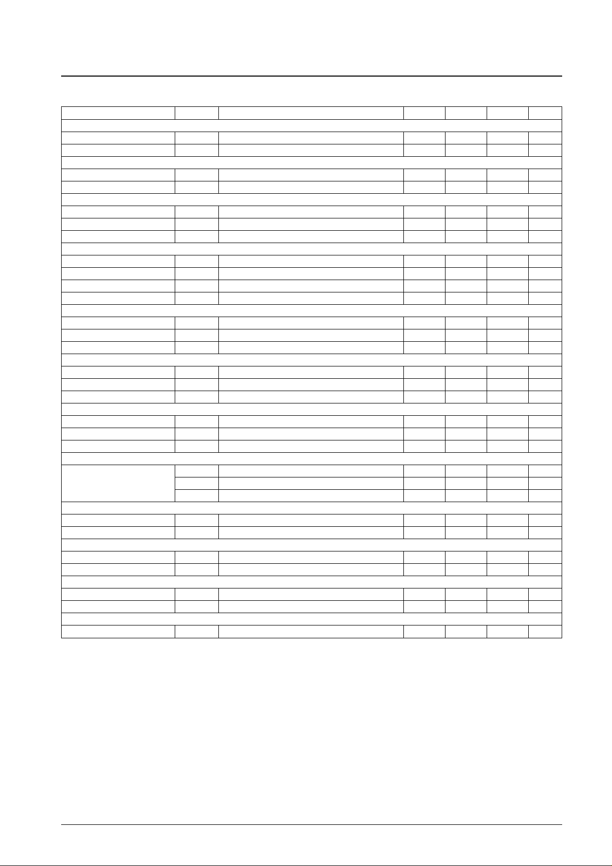
Continued from preceding page.
No. 4845-3/9
LB1825
Parameter Symbol Conditions min typ max Unit
[FG switching setting]
Single Hall FG operating level V
FGIH
FGINpin voltage V
REG
– 0.1 V
REG
V
Triple Hall FG operating level V
FGIL
FGINpin voltage 0 0.1 V
[Stop mode setting]
FG
OUT
1 low level voltage V
FG1
L 0.4 V
FG
OUT
1 low level current I
FG1
L FG
OUT
1 pin voltage = 0 V 0.6 2.4 mA
[Current limiter]
Reference voltage V
CS
R = 47 kΩ 0.51 0.58 0.65 V
External supply range V
CS
(EX) 0.7 3.0 V
Offset voltage V
CSO
R = 47 kΩ, Rf= 1.8 Ω 25 50 90 mV
[Signal block]
Internal oscillator frequency f
OSC
Crystal oscillator mode 1 12 MHz
External input frequency f
REF
External clock mode 30 5000 Hz
Low level pin voltage V
OSCL
4.0 4.5 5.0 V
High level pin current I
OSCH
0.3 0.5 0.75 mA
[Divisor switching]
Input high level voltage V
N1 to 3
H 4.2 V
REG
V
Input middle level voltage V
N1 to 3
M 2.1 2.9 V
Input low level voltage V
N1 to 3
L 0 0.8 V
[F/R switching]
Input high level voltage V
FRH
2.4 V
REG
V
Input low level voltage V
FRL
0 1.5 V
High level input current I
FRH
F/R pin voltage = V
REG
0.22 mA
[S/B switching]
Input high level voltage V
SBH
2.4 V
REG
V
Input low level voltage V
SBL
1.5 V
Hysteresis (high → low) DV
SB
0.15 0.25 0.35 V
[Stop detection]
S
CT
1 FG mode 32
Count setting S
CT
2 Triple Hall FG mode 8
S
CT
3 Single Hall FG mode 2
[Undervoltage protection]
Operating voltage V
SD
8.4 8.8 9.2 V
Hysteresis DV
SD
0.2 0.4 0.6 V
[Thermal protection]
Operating temperature T
SD
Design target value 150 180 °C
Recovery temperature T
SDR
Design target value 140 °C
[Pin leakage currents]
LD pin I
LD (LEAK)
Pin voltage = 30 V 10 µA
FG
OUT
2 pin I
FG2 (LEAK)
Pin voltage = 30 V 10 µA
[GND pin-heat sink]
Resistance Design target value. 30 Ω
Page 4
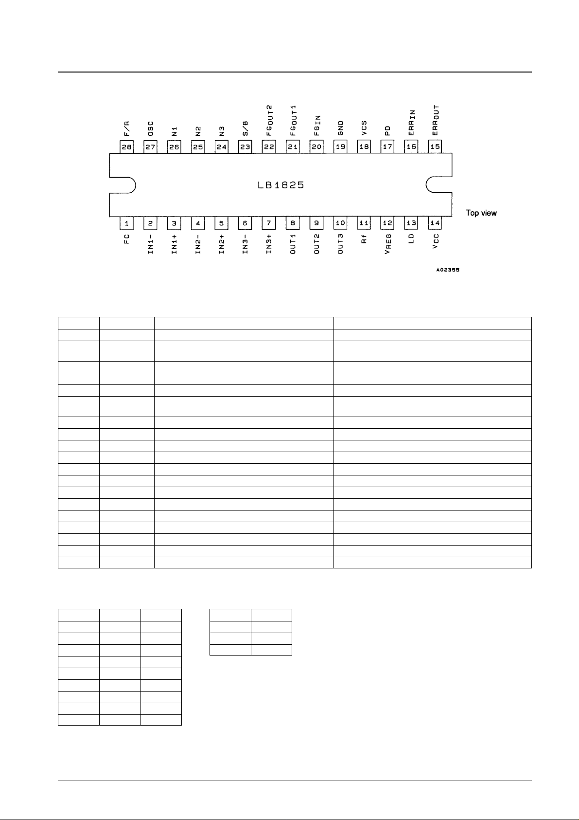
Pin Assignment
Pin Functions
Clock Divisor Switching
Note: I. Total divisor = (divisor (1) × divisor (2))
PLL servo frequency = (crystal oscillator frequency)/(total divisor)
II. External clock mode
The PLL servo frequency = external input frequency
No. 4845-4/9
LB1825
Pin No. Symbol Function Notes
1 FC Frequency characteristics correction A capacitor must be inserted between pin 1 and ground.
2 to 7
IN1
+
to IN3+,
Hall element inputs Taken as high when IN
+
> IN–, and as low otherwise.
IN1
–
to IN3
–
8 to 10 OUT1 to OUT3 Outputs
11 R
f
Output current detector A capacitor must be inserted between pin 11 and ground.
12 V
REG
Stabilized power supply output
13 LD Phase lock detector output
On when the phase is locked. This pin is an open-collector
output.
14 V
CC
Power supply
15 ERR
OUT
Error amplifier output
16 ERR
IN
Error amplifier input
17 PD Phase comparator output
18 V
CS
Current limiter reference voltage generation
19 GND Ground
20 FG
IN
FG amplifier input Also functions as the Hall FG switching pin.
21 FG
OUT
1 FG amplifier output The LB1825 goes to stop mode when pin 21 is set low.
22 FG
OUT
2 FG/Hall FG output This pin is an open-collector output.
23 S/B Brake command input Braking is applied when pin 23 is set high.
24 to 26 N1 to N3 Reference frequency divisor switching The clock divisor is set by the states of pins 24 to 26.
27 OSC Crystal oscillator/external clock input
28 F/R Forward/reverse switching
Pin N1 Pin N2 Divisor (1)
*I
L L *II
L M 128
L H 256
M L 512
M M 1024
M H 2048
H L 4096
H M 8192
H H 16384
Pin N3 Divisor (2)
*I
L 5
M 4
H 3
Page 5
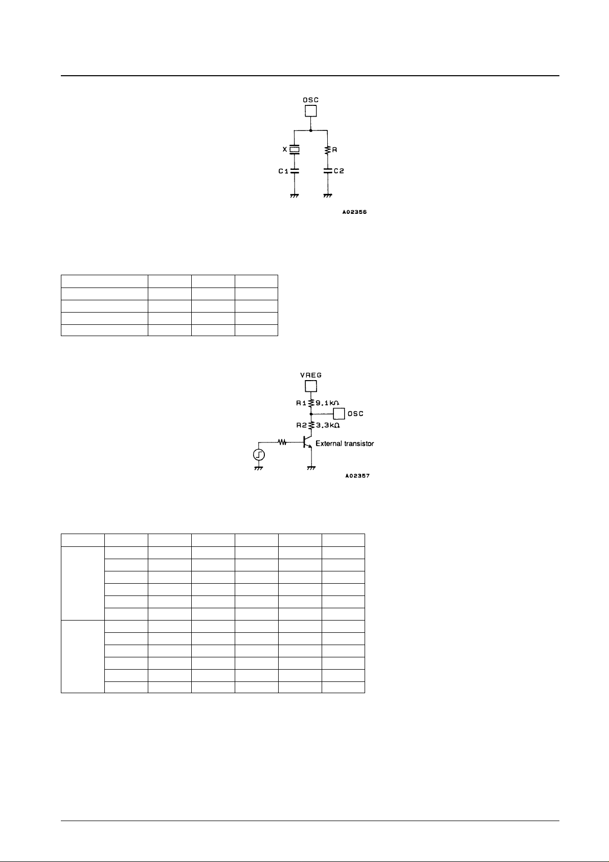
Figure 1 Pin Circuit for Internal Clock Mode
Table 1: External Component Values (reference values)
Use a crystal that has a ratio of at least 1:5 between the fundamental f0 impedance and the 3f0 impedance.
Figure 2 Pin Circuit for External Clock Mode
F/R Switching and Phase Selection
Columns OUT1 to OUT3
H: Source
L: Sink
No. 4845-5/9
LB1825
Crystal (MHz) C1 (pF) C2 (pF) R (kΩ)
3 to 4 39 82 0.82
4 to 5 39 82 1.0
5 to 7 39 47 1.5
7 to 10 39 27 2.0
F/R IN1 IN2 IN3 OUT1 OUT2 OUT3
H H L M H L
H L L H M L
L
H L H H L M
L L H M L H
L H H L M H
L H L L H M
H H L M L H
H L L L M H
H
H L H L H M
L L H M H L
L H H H M L
L H L H L M
Page 6
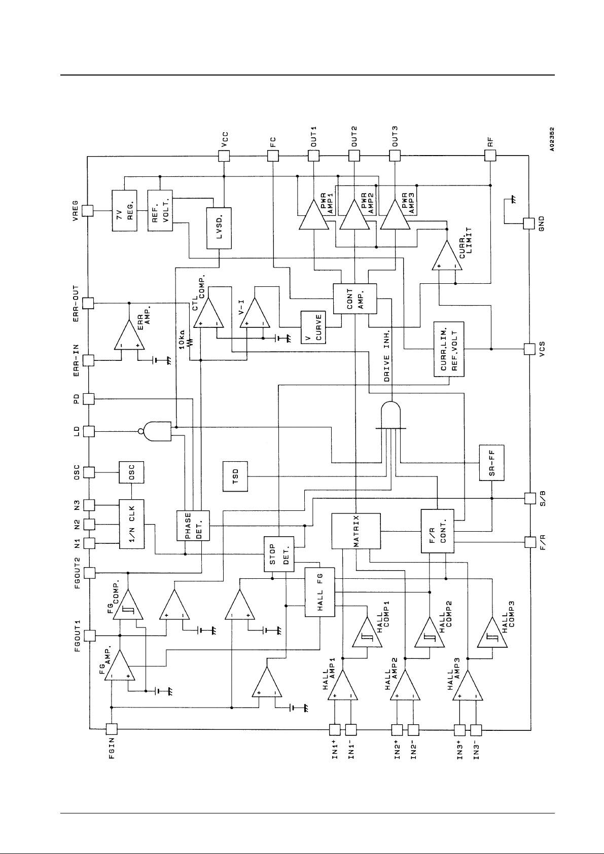
Equivalent Circuit Block Diagram
No. 4845-6/9
LB1825
Page 7
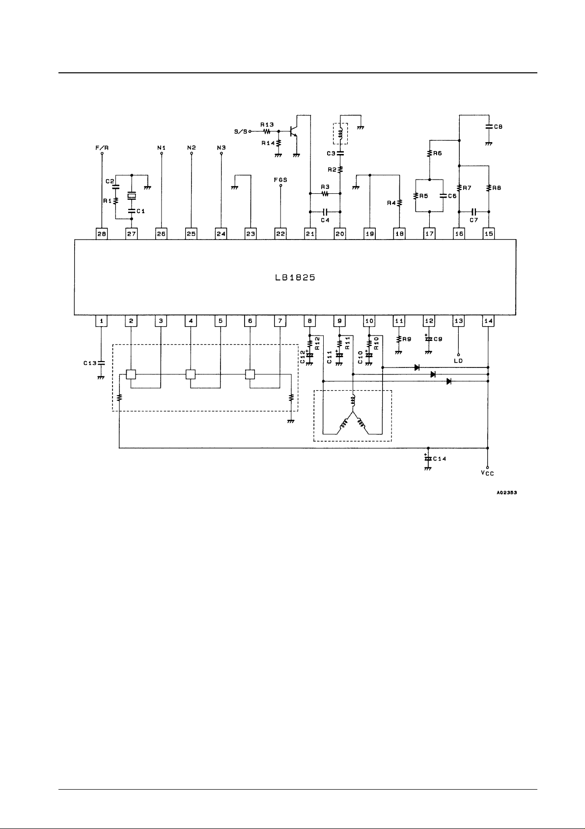
Sample Application Circuit (Polygon Mirror Motor)
No. 4845-7/9
LB1825
Page 8
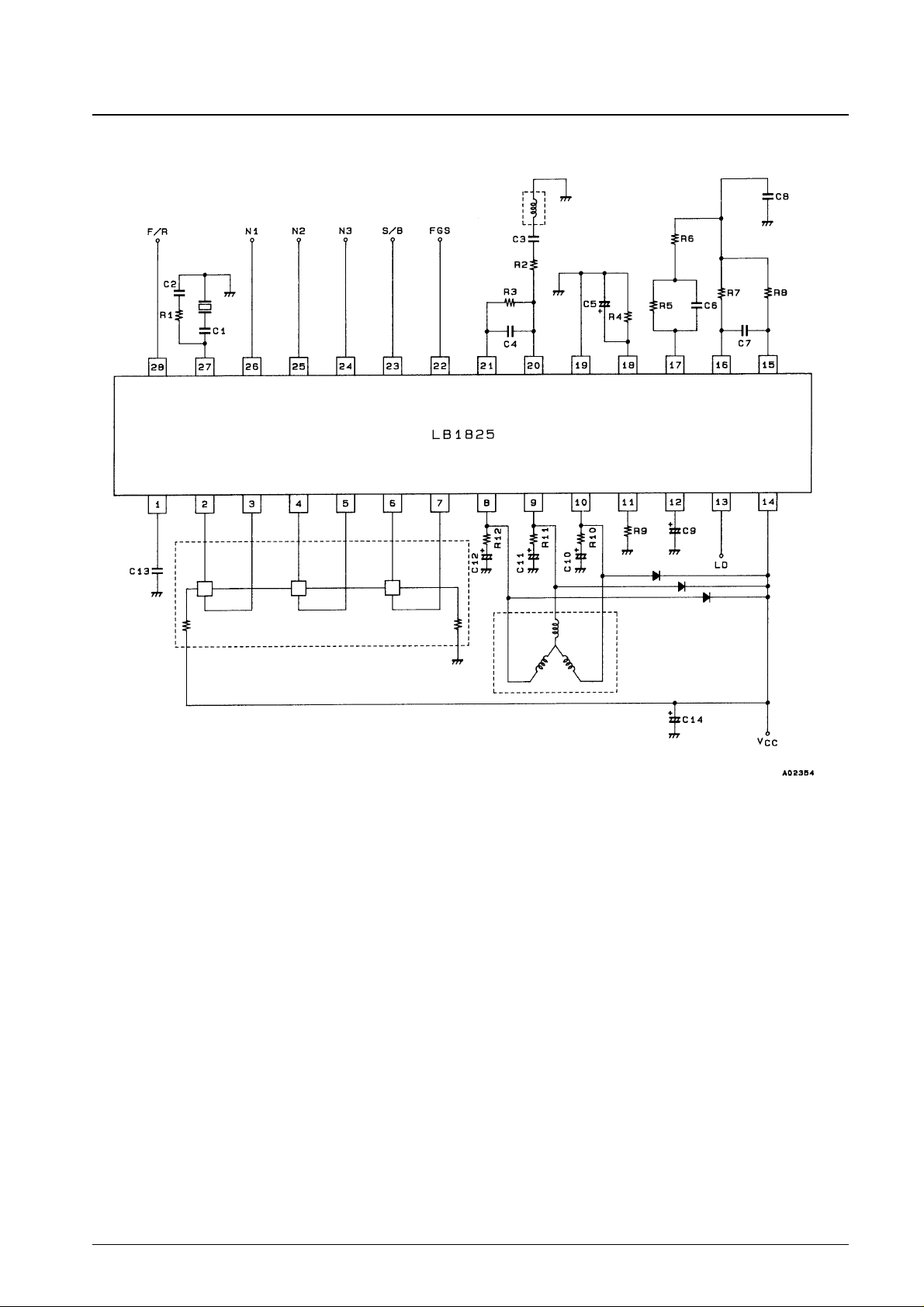
Sample Application Circuit (Optical Disk Spindle Motor)
Usage Notes
1. Position detector circuit (Hall element input circuit)
The position detection circuit consists of a differential amplifier, and will operate if a differential input of 40 mVp-p
(minimum) is provided. However, an input of 100 mVp-p is desirable from the standpoint of noise and other
problems.
The input DC level must be within the common mode input voltage range (1.5 to (VCC– 1.8) V).
2. Current limiter circuit
The output current limiter operates by holding the sink side output transistor in an unsaturated state.
The current limit value can be calculated from the following formula.
I = VCS/R
f
Where: VCS= 0.58 V typical, Rf= The value of the resistor between pin 11 and ground.
3. FG input
The following three methods can be used to input the speed signal FG from the motor.
• The signal can be input to FGINthrough an amplifier. (FG mode)
• The Hall input IN1 can be used as the FG input. (single Hall FG mode)
This is set up by connecting FGINto V
REG
.
• The composite signal from the IN1, IN2 and IN3 Hall inputs can be used as the FG input. (triple Hall FG mode)
This is set up by connecting FGINto ground.
No. 4845-8/9
LB1825
Page 9

No. 4845-9/9
LB1825
4. Reference signal input circuit
• Internal clock mode (crystal oscillator)
The values of the external components associated with the crystal oscillator must be set up according to the
frequency of the oscillator. (See Table 1.) To avoid trouble with the oscillator circuit, confirm the component
values used with the oscillator’s manufacturer.
• External clock mode
Use the external circuit shown in Figure 2 to input the clock signal when controlling the motor speed using a
reference signal with the same frequency as FG.
5. Start/stop
When driving motors such as polygon mirror motors, the motor is normally stopped by turning off motor drive and
putting the motor in the free-running state. For this type of motor, set the S/B pin low and attach an external
transistor at FG
OUT
1 as shown in the Sample Application Circuit (Optical Disk Spindle Motor) figure to start and
stop the drive. (Motor drive is turned off when FG
OUT
1 is low.)
6. Start/brake
When driving motors such as optical disk spindle motors, stopping is performed by applying some form of braking.
In these applications it is necessary for the motor to decelerate briefly and come to a complete stop. See the Sample
Application Circuit (Optical Disk Spindle Motor) figure for a sample circuit for this case. (The difference between
this circuit and the circuit shown in the Sample Application Circuit (Optical Disk Spindle Motor) figure is the
addition of the capacitor C5 to the S/B pin start/brake circuit.)
Braking Operation
This braking circuit applies full torque reverse rotation braking (in the current limited state) directly after the S/B pin is
set low while the motor is turning. After that, the reverse torque is gradually decreased (according to the time constant
determined by R4 and C5) at the points where the speed falls below the values listed below. This operation brings the
disk to a full stop.
f3H = fFG/32 (FG mode)
f3H = fFG/8 (Triple Hall FG mode) f3H: Triple Hall input composite frequency.
f3H = fFG/2 (Single Hall FG mode) fFG: The FG frequency when locked
Depending on the size of the disk and the motor torque the following adjustments may be required to improve the disk
stopping characteristics.
1. Increase the time constant if the motor continues to rotate in the forward direction after the braking torque has gone
to zero.
2. Decrease the time constant if the motor is observed to rotate in the reverse direction due to the braking operation.
3. A value of about 51 kΩis recommended for R4. In particular, it should be under 100 kΩ.
This catalog provides information as of August, 1997. Specifications and information herein are subject to
change without notice.
■ No products described or contained herein are intended for use in surgical implants, life-support systems, aerospace
equipment, nuclear power control systems, vehicles, disaster/crime-prevention equipment and the like, the failure of
which may directly or indirectly cause injury, death or property loss.
■ Anyone purchasing any products described or contained herein for an above-mentioned use shall:
➀ Accept full responsibility and indemnify and defend SANYO ELECTRIC CO., LTD., its affiliates, subsidiaries and
distributors and all their officers and employees, jointly and severally, against any and all claims and litigation and all
damages, cost and expenses associated with such use:
➁ Not impose any responsibility for any fault or negligence which may be cited in any such claim or litigation on
SANYO ELECTRIC CO., LTD., its affiliates, subsidiaries and distributors or any of their officers and employees
jointly or severally.
■ Information (including circuit diagrams and circuit parameters) herein is for example only; it is not guaranteed for
volume production. SANYO believes information herein is accurate and reliable, but no guarantees are made or implied
regarding its use or any infringements of intellectual property rights or other rights of third parties.
 Loading...