

Page 1

Ordering number: EN3950C
Monolithic Digital IC
LB1839M
Low-voltage/Low-saturation Bidirectional
Constant-Voltage Regulated Motor Driver
Overview
The LB1839M is a low-voltage, low-saturation, three-input
type two-channel bidirectional motor driver that permits
switching between constant-voltage regulated output and
saturated output. The design of the LB1839M is ideal for a
two-phase bipolar driver for stepping motors.
Features
.
Wide operating voltage range (3.0 to 9.0 V).
.
Low saturation voltage
V
(sat) = 0.40 V at IO= 200 mA.
O
.
Consumes almost no current in standby mode
(0.1 µA or less).
.
Permits setting of bidirectional constant-voltage regulated
value.
.
Three-input type that is ideal for a two-phase bipolar driver.
.
Permits switching between constant-voltage regulated output
and saturated output.
.
Built-in reference voltage coupled to input.
.
Compact MFP14S package.
Package Dimensions
unit: mm
3111-MFP14S
[LB1839M]
SANYO : MFP14S
Specifications
Absolute Maximum Ratings atTa=25°C
Parameter Symbol Conditions Ratings Unit
Maximum supply voltage V
Output current Im max 250 mA
Applied input voltage V
Allowable power dissipation Pd max With board ( 30 x 30 x 1.5 mm
Operating temperature Topr –20 to +80
Storage temperature Tstg –40 to +125
max 10.5 V
CC
IN
3
) 800 mW
–0.3 to +10 V
Allowable Operating Ranges atTa=25°C
Parameter Symbol Conditions Ratings Unit
Supply voltage V
Input [H] voltage V
Input [L] voltage V
Control voltage V
CC
IH
IL
C
3.0 to 9.0 V
3.0 to 9.0 V
–0.3 to +0.7 V
0.2 to 6.0 V
SANYO Electric Co.,Ltd. Semiconductor Bussiness Headquarters
TOKYO OFFICE Tokyo Bldg., 1-10, 1 Chome, Ueno, Taito-ku, TOKYO, 110 JAPAN
81095HA(II)/61295HA(II)/5072TS No.3950-1/5
C
°
C
°
Page 2

LB1839M
Electrical Characteristics atTa=25°C, VCC=6V
Parameter Symbol Conditions min typ max Unit
Supply current I
Output saturation voltage Vsat1 I
Reference voltage Vref Ivref=1mA 1.85 2.0 2.15 V
Output voltage
voltage characteristics
Output voltage
current characteristics
Input current I
Output voltage V
Equivalent Circuit Block Diagram
(For one channel)
0 During standby 0.1 10 µA
CC
I
CC
I
CC
Vsat2 I
Vsat3 I
∆V
∆V
∆V
∆I
CC
IN
(For two channel) During bidirectional operation,
1
(For two channel) During bidirectional operation,
2
= 100 mA (upper side + lower side) 0.30 0.40 V
O
= 200 mA (upper side + lower side) 0.40 0.55 V
O
= 200 mA (lower side) 0.07 0.10 0.15 V
O
VO=5V,VCC= 5.5 to 9 V,
O
I
= 100 mA
CC
O
VO=5V,VCC=6V,
O
I
=10to100mA
O
during control, load open
during saturation, load open
VIN= 5 V 90 150 µA
Between OUT and GND
O
2.5xV
C
3.5 5.0 mA
4.0 6.0 mA
2.7xVCV
20 mV
50 mV
Thermal
Reference
voltage
Logic predriver
Truth Table
Input Output
ENA IN 1/2 VM 1/2
L — — OFF OFF Standby
HLLHL
HLHHL
HHL LH
HHHLH
OUT
1/3
OUT
2/4
The constant-voltage regulated output VO(= voltage between H
side output and GND) is controlled by 2.5 x V
in the saturated state when the V
V
^ VCC.
O
input range is 0.2 to 6 V and
C
Mode
Constant-voltage
regulated forward
operation
Saturated
forward operation
Constant-voltage
regulated reverse
operation
Saturated
reverse operation
. The output is
C
Pin Assignment
Note: Both GND pins must be grounded.
No.3950 -2/5
Page 3
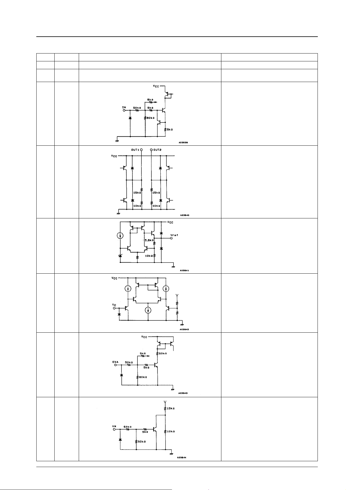
Pin Functions
LB1839M
Pin No.
14 V
9
12
3
6
8
10
11
13
4 Vref
Symbol Equivalent Circuit Diagram Pin Function
CC
Power supply pin for output and controller.
GND GND pins for output and controller. Both
must be grounded.
IN2
IN1
Input pins that determine the excitation of
the outputs.
IN1 control outputs OUT1 and OUT2; IN2
control outputs OUT3 and OUT4.
L: –0.3 to +0.7 V
H: 3.0 to 9.0 V
There are no limitations on the magnitude
OUT4
OUT3
relationships between the V
supply voltages.
Output pins.
Have built-in spark killer diodes.
CC
and V
OUT1
OUT2
Reference voltage (= 2.0 V).
IN
5V
C
2 ENA
1
VM1
7
VM2
Output
Output
Input pins that determine the constantvoltage regulated output level.
The constant-voltage regulated output V
(= voltage between H side output and
GND) is controlled by V
are no limitations on the magnitude
relationships between the V
supply voltages.
=2.5xVC. There
O
and V
CC
C
Standby/drive control input pin
Current consumption in standby mode is
10 µA or less.
L: –0.3 to + 0.7 V
H: 3.0 to 9.0 V
Output voltage setting
Control input pin for switching between
constant voltage output and saturated
output. There are no limitations on the
magnitude relationships between the V
V
and VM2supply voltages.
M1
L: –0.3 to + 0.7 V
(constant-voltage regulated output)
H: 3.0 to 9.0 V (saturated output)
CC
O
,
No.3950 -3/5
Page 4
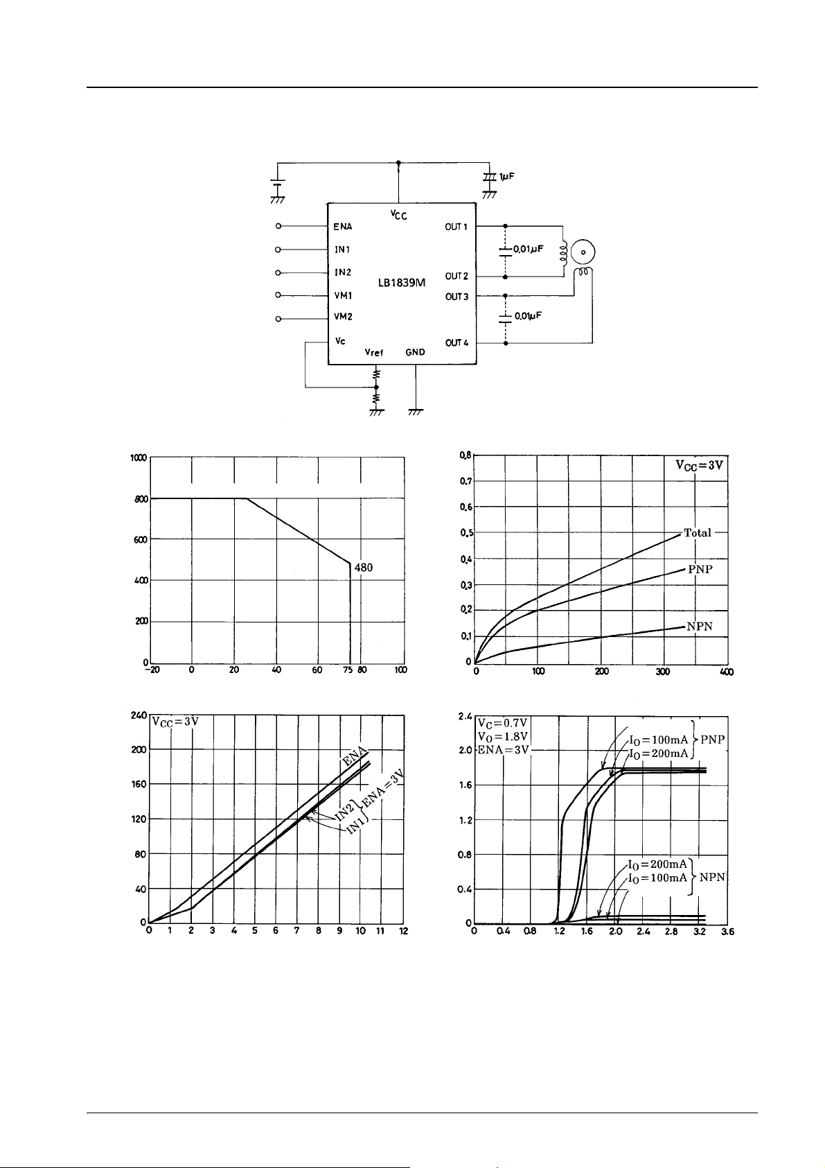
Sample Application Circuit
LB1839M
Stepping motor
If the outputs oscillate, insert capacitors
of 0.001 to 0.1 µF between the outputs.
Pd max — Ta
Specified board (30 x 30 x 1.5 mm3glass epoxy)
Allowable power dissipation, Pd max — mW
Ambient temperature, Ta —°C
I
—V
IN
—µA
IN
VO(sat) — I
(sat) — V
O
Output saturation voltage, V
Output current, I
IN
VO—V
O
—mA
O
CC
No load
—V
O
Input current, I
Output voltage, V
No load
Input voltage, V
IN
—V
Supply voltage, VCC—V
No.3950 -4/5
Page 5
LB1839M
No products described or contained herein areintendedforuse in surgical implants, life-support systems, aerospace equipment,
nuclear power control systems, vehicles, disaster/crime-prevention equipment and the like, the failure of which may directly or
indirectly cause injury, death or property loss.
Anyone purchasing any products described or contained herein for an above-mentioned use shall:
1 Accept full responsibility and indemnify and defend SANYO ELECTRIC CO., LTD., its affiliates, subsidiaries and distributors
and all their officers and employees, jointly and severally, against any and all claims and litigation and all damages, cost and
expenses associated with such use:
2 Not impose any responsibility for any fault or negligence which may be cited in any such claim or litigation on SANYO
ELECTRIC CO., LTD., its affiliates, subsidiaries and distributors or any of their officers and employees jointly or severally.
Information (including circuit diagrams and circuit parameters) herein is for example only; it is not guaranteed for volume
production. SANYO believes information herein is accurate and reliable, but no guarantees are made or implied regarding its use
or any infringements of intellectual property rights or other rights of third parties.
This catalog provides information as of June, 1995. Specifications and information herein are subject to change without notice.
No.3950 -5/5
 Loading...