

Page 1
Overview
The LB1910 is a 3-phase disc drive motor driver that is
optimal for use as a 3.5-inch FDD spindle motor driver.
Functions and Features
• Three-phase full-wave linear driver
• Digital speed control circuit
• Start and stop circuits (active low)
• RPM switching H: 300 rpm
L: 360 rpm
• Current limiter circuit
• Built-in index comparator
• Thermal shutdown circuit
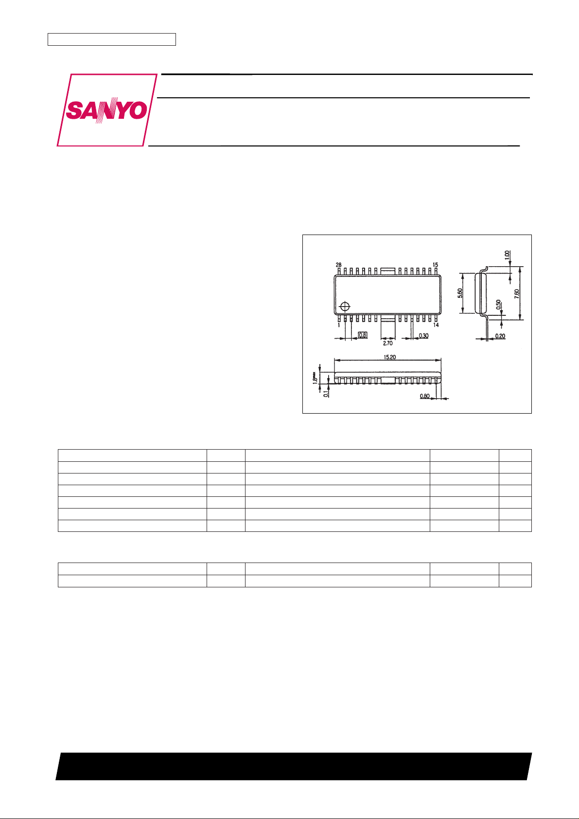
Package Dimensions
unit: mm
3222-HSOP28
Monolithic Digital IC
43096HA (OT) No. 5383-1/7
SANYO: HSOP28
[LB1910]
SANYO Electric Co.,Ltd. Semiconductor Bussiness Headquarters
TOKYO OFFICE Tokyo Bldg., 1-10, 1 Chome, Ueno, Taito-ku, TOKYO, 110 JAPAN
FDD Spindle Motor Driver
LB1910
Ordering number : EN5383
Parameter Symbol Conditions Ratings Unit
Maximum supply voltage V
CC
max 7.0 V
Maximum output current I
O
max1 t ≤ 0.5 s 1.0 A
Maximum steady-state output current I
O
max2 0.7 A
Allowable power dissipation Pd max Independent IC 0.5 W
Operating temperature Topr –20 to +80 °C
Storage temperature Tstg –40 to +150 °C
Specifications
Absolute Maximum Ratings at Ta = 25°C
Parameter Symbol Conditions Ratings Unit
Recommended supply voltage V
CC
4.2 to 6.5 V
Allowable Operating Ranges at Ta = 25°C
Page 2

No. 5383-2/7
LB1910
Electrical Characteristics at Ta = 25°C, VCC= 5 V
Parameter Symbol Conditions min typ max Unit
Current drain
I
CCO
S/S = 5 V (standby) 10 µA
I
CC
S/S = 0 V (steady state) 12 18 mA
SL bias current I
SL
VSL= 0 V 10 µA
SL input low-level voltage V
SLL
0 1.0 V
SL input high-level voltage V
SLH
3.5 V
CC
V
S/S bias current I
S/S
180 270 µA
S/S low-level voltage V
S/SL
0 0.8 V
S/S high-level voltage V
S/SH
3.5 V
CC
V
Hall amplifier input bias current I
HB
10 µA
Common-mode input voltage
V
h
1.5 VCC– 1.0 V
range
Differential input voltage range Vdif 50 200 mVp-p
Hall bias output voltage V
H
IH= 5 mA 0.8 V
Leakage current I
HL
S/S = 5 V ±10 µA
Output saturation voltage Vsat I
O
= 0.7 A, sink + source 1.3 1.8 V
Output leakage current I
OL
1.0 mA
Current limiter Vlim 0.27 0.3 0.33 V
Control amplifier voltage gain G
C
–7 dB
Voltage gain difference between
∆G
C
±1 dB
phases
V/I conversion source current I
+
9 14 19 µA
V/I conversion sink current I
–
–9 –14 –19 µA
V/I conversion current ratio I
+/I–
0.8 1.0 1.2
DSC buffer input current I
DSC
1.0 µA
FG Schmitt hysteresis ∆Vsh * 50 mV
Speed discriminator counts N 1041.5
Discriminator operating frequency F
D
* 1.1 MHz
Oscillator frequency range F
OSC
* 1.1 MHz
Index output low-level voltage V
IDLIO
= 2 mA 0.4 V
Index output leakage current I
IDL
±10 µA
FG amplifier voltage gain G
FG
* 48 dB
FG amplifier input offset V
FG O
±10 mV
FG amplifier internal reference
V
FG B
2.2 2.5 2.8 V
voltage
Thermal shutdown temperature TSD * 150 180 °C
Hysteresis ∆TSD * 40 °C
Note: * Items marked with an asterisk are design target values and are not measured.
Page 3

Pin Assignment
Truth Table
No. 5383-3/7
LB1910
Source → sink
Hall input
U V W
1 V phase → W phase H H L
2 V phase → U phase L H L
3 W phase → U phase L H H
4 W phase → V phase L L H
5 U phase → V phase H L H
6 U phase → W phase H L L
Note: Hall input high levels are defined as: U
IN
+
> U
IN
–
V
IN
+
> V
IN
–
W
IN
+
> W
IN
–
Page 4
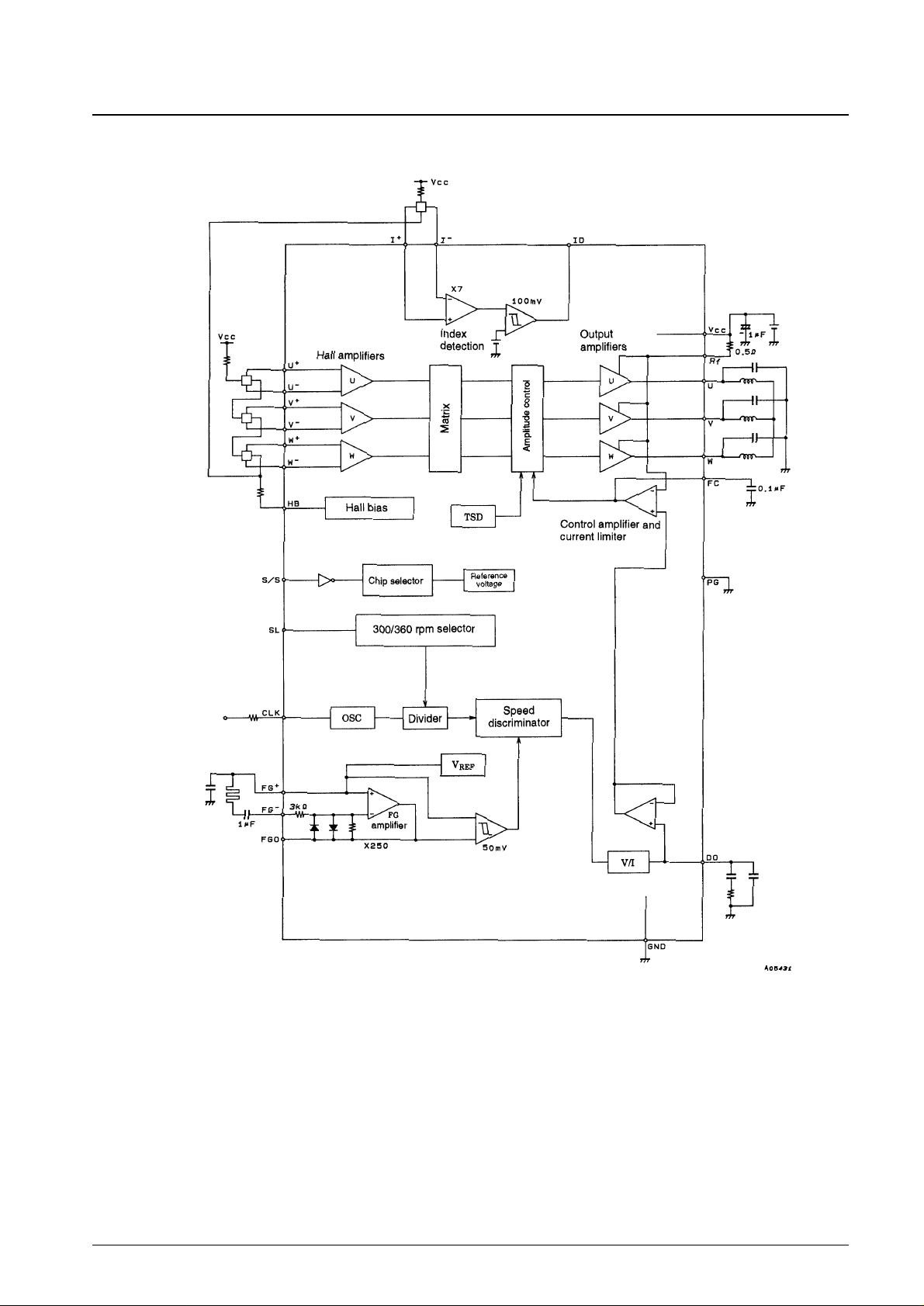
Block Diagram
No. 5383-4/7
LB1910
Page 5
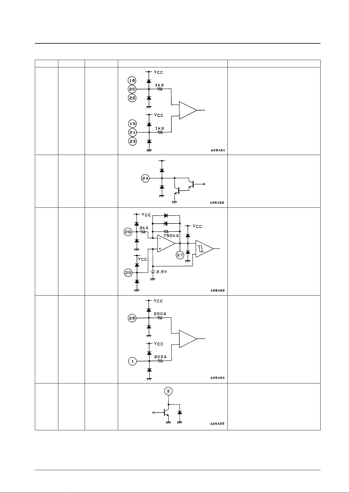
Pin Functions
No. 5383-5/7
LB1910
Pin No. Symbol Pin voltage Equivalent circuit diagram Function
Index output
L: 0.4 V max
H: 4.5 V min
ID2
Index input
I
+
I
–
28
1
• FG amplifier plus input
A 2.5-V reference voltage is generated
internally.
• FG amplifier minus input
• FG amplifier output
2.5 V
FG
IN
+
FG
IN
–
FG
OUT
25
26
27
Minus side connection for providing the Hall bias
current
This pin becomes open in the stopped state, thus
cutting the Hall bias current.
0.8 V typ
(I
H
= 5 mA)
HB24
U phase Hall element input
V phase Hall element input
W phase Hall element input
1.5 V min
V
CC
– 1.0 V
max
U
IN
+
U
IN
–
V
IN
+
V
IN
–
W
IN
+
W
IN
–
18
19
20
21
22
23
Continued on next page.
Page 6
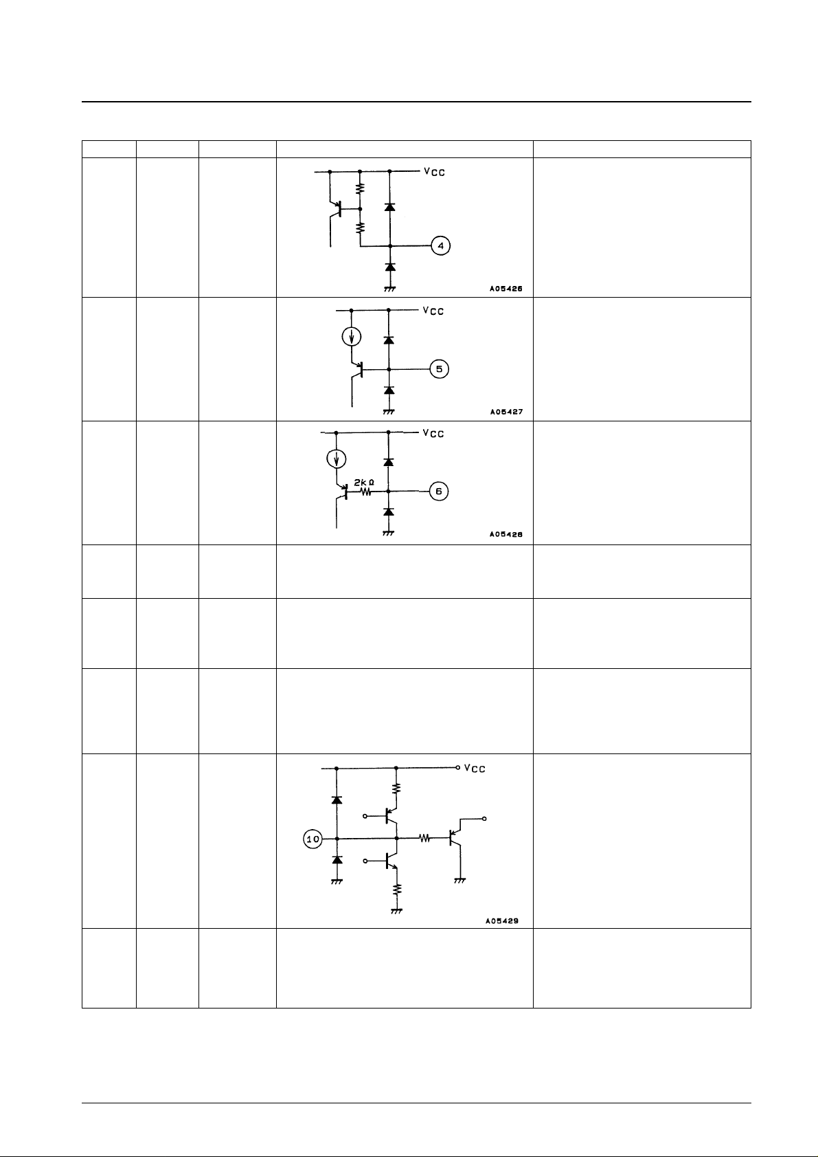
No. 5383-6/7
LB1910
Continued from preceding page.
Pin No. Symbol Pin voltage Equivalent circuit diagram Function
Frequency characteristics compensation
Current control system loop oscillation is
prevented by connecting a capacitor between
this pin and ground.
F
C
11
Speed discriminator
D
O
10
Output current detection
The output current is detected as a voltage by
connecting the resistor Rf between this pin and
V
CC
. The current limiter operates by detecting
the voltage on this pin.
Rf9
Power supply
This voltage must be stabilized so that ripple and
noise do not enter the IC.
V
CC
8
• Ground
• This pin, pin 14, and the frame must all be
grounded together.
GND7
Reference clock input
A 1-MHz input frequency corresponds to speeds
of 300 and 360 rpm.
L: 1.0 V max
H: V
CC
– 1.0 V
min
CLK6
Rotational speed switching
L: 1.0 V max
H: 3.5 V min
SL5
Start/stop mode switching
This is an active-low input.
L: 0.8 V max
H: 3.5 V min
SS4
Continued on next page.
Page 7
No. 5383-7/7
LB1910
This catalog provides information as of December, 1997. Specifications and information herein are subject to
change without notice.
■ No products described or contained herein are intended for use in surgical implants, life-support systems, aerospace
equipment, nuclear power control systems, vehicles, disaster/crime-prevention equipment and the like, the failure of
which may directly or indirectly cause injury, death or property loss.
■ Anyone purchasing any products described or contained herein for an above-mentioned use shall:
➀ Accept full responsibility and indemnify and defend SANYO ELECTRIC CO., LTD., its affiliates, subsidiaries and
distributors and all their officers and employees, jointly and severally, against any and all claims and litigation and all
damages, cost and expenses associated with such use:
➁ Not impose any responsibility for any fault or negligence which may be cited in any such claim or litigation on
SANYO ELECTRIC CO., LTD., its affiliates, subsidiaries and distributors or any of their officers and employees
jointly or severally.
■ Information (including circuit diagrams and circuit parameters) herein is for example only; it is not guaranteed for
volume production. SANYO believes information herein is accurate and reliable, but no guarantees are made or implied
regarding its use or any infringements of intellectual property rights or other rights of third parties.
Continued from preceding page.
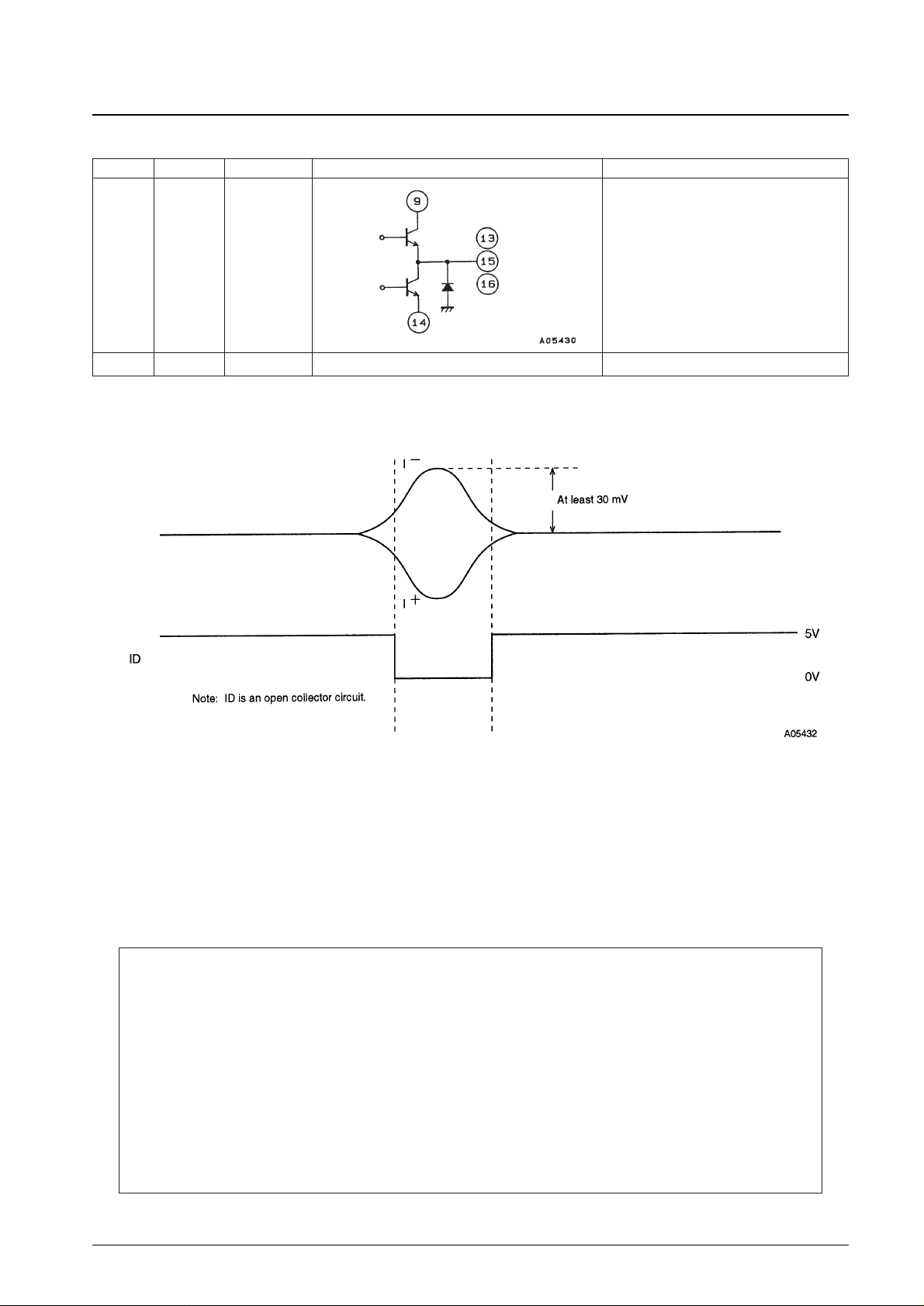
Index Pulse Timing Chart
Pin No. Symbol Pin voltage Equivalent circuit diagram Function
Output transistor ground connectionPGND14
U phase output
V phase output
W phase output
U
OUT
V
OUT
W
OUT
13
15
16
 Loading...