

Page 1
Ordering number: EN5243
Monolithic Digital IC
LB1694N
3-phase Brushless Motor Driver
Overview
The LB1694N is a 3-phase brushless motor driver IC that is
ideal for driving DC fan motors in air conditioners, hot-water
supply systems, and the like.
Package Dimensions
unit : mm
3037A-DIP20H
[LB1694N]
Features
.
3-phase brushless motor driver.
.
Withstand voltage: 45 V; output current: 2.5 A.
.
Current limiter built in.
.
Low-voltage protector circuit built in.
.
Thermal shutdown protector built in.
.
Hall amplifier with hysteresis built in.
.
FG output function.
SANYO : DIP20H
Specifications
Absolute Maximum Ratings atTa=25°C
Parameter Symbol Conditions Ratings Unit
V
max 10 V
Maximum supply voltage
Output current I
Allowable power dissipation
Operating temperature Topr –20 to +100
Storage temperature Tstg –55 to +120
CC
V
max 45 V
M
O
Pd max1 Independent IC 2.2 W
Pd max2 With arbitrarily large heat sink 15.2 W
2.5 A
C
°
C
°
Allowable Operating Ranges atTa=25°C
Parameter Symbol Conditions Ratings Unit
V
Supply voltage range
Power supply voltage rise rate
*1 If the supply voltage rise rate is fast when power is applied, through current may flow to output.
CC
V
M
∆V
/ ∆tVCC=V
CC
∆V
/ ∆tVM= 0 V point*1 to 0.16 V/µs
M
(OFF) point *1 to 0.04 V/µs
LVSD
SANYO Electric Co.,Ltd. Semiconductor Bussiness Headquarters
TOKYO OFFICE Tokyo Bldg., 1-10, 1 Chome, Ueno, Taito-ku, TOKYO, 110 JAPAN
D3095HA (II) No.5243-1/8
4.5 to 5.5 V
5to42 V
Page 2
LB1694N
With arbitrarily large
heat sink
Independent IC
Allowable power dissipation, Pd max — W
Ambient temperature, Ta —°C
Electric Characteristics atTa=25°C, VCC=5V,VM=30V
Parameter Symbol Conditions min typ max Unit
Supply current I
Output saturation voltage
Output leak current I
CC
V
Osat1IO
V
Osat2IO
O(leak)
Hall amplifier
Input bias current I
Common-mode input voltage
range
HB
V
ICM
Hysteresis width ∆V
Input voltage L → HV
Input voltage H → LV
SLH
SHL
FG pin (rate pulse output)
Low level output voltage V
Pull-up resistance R
F/R operation Forward V
F/R operation Reverse V
Current limit operation limiter V
Thermal shutdown operation
temperature
FGL
FR1
FR2
T
FG
RF
SD
Hysteresis width ∆T
Reduced voltage protection
operation voltage
Reduced voltage protection
release voltage
Hysteresis width ∆V
C pin charge current I
C pin discharge current I
C pin charge start voltage V
C pin discharge start voltage V
Output current neglect time t
Output off time t
V
LVSD
V
LVSD(OFF)
LVSD
CL
CH
CL
CH
sm
so
Forward 13 19 mA
= 1 A, VO(sink) + VO(source) 2.1 3.0 V
= 2 A, VO(sink) + VO(source) 3.0 4.2 V
IN
IFG= 5 mA 0.4 V
Design target 120 150
Design target 30
SD
R=33kΩ 30 40 50 µA
R=33kΩ 90 120 150 µA
R=33kΩ 0.3 0.4 0.5 V
R=33kΩ 1.5 2.0 2.5 V
R=33kΩ, C = 4700 pF 58 68 78 µs
R=33kΩ, C = 4700 pF 164 193 222 µs
100 µA
14µA
1.5 3.2 V
21 30 37 mV
515 25mV
–25 –15 –5 mV
7.5 10 12.5 kΩ
0 0.8 V
4.2 5.0 V
0.42 0.5 0.6 V
3.5 3.8 4.1 V
4.3 4.5 V
0.4 0.5 0.6 V
C
°
C
°
No.5243-2/8
Page 3

Truth Table
Input F/R control Output FG output
IN1 IN2 IN3 F/R Source → Sink FG1 FG2
1HLH
2HLL
3HHL
4LHL
5LHH
6LLH
LB1694N
L OUT2 → OUT1
H OUT1 → OUT2
L OUT3 → OUT1
H OUT1 → OUT3
L OUT3 → OUT2
H OUT2 → OUT3
L OUT1 → OUT2
H OUT2 → OUT1
L OUT1 → OUT3
H OUT3 → OUT1
L OUT2 → OUT3
H OUT3 → OUT2
LL
LH
LL
HH
HL
HH
F/R
Forward L 0.0 to 0.8 V
Reverse H 4.2 to 5.0 V
Pin Assignment
FG output
FG1
FG2
No.5243-3/8
Page 4
LB1694N
Block Diagram and Peripheral Circuit Diagram
No.5243-4/8
Page 5
Pin Functions
LB1694N
Pin No.
Pin Name Pin Voltage Equivalent Circuit Diagram Pin Function
1V
CC
2R
Supplies power to all circuits except output
block.
Sets the C pin charge/discharge current.
3C Sets the output off time and output current
neglect time during current limiter operation.
5
OUT1
6
OUT2
7
OUT3
Output pin 1
Output pin 2
Output pin 3
8RF Output current detection pin. By inserting
resistor R
output current is detected as voltage. The
between this pin and GND, the
f
output current is limited to a current value set
10 V
by V
M
Power supply pin providing output.
(current limit operation).
RF/Rf
11 GND GND for other than output.
The minimum potential of output transistor is
the RF pin voltage.
12 F/R 0.0 V min
V
max
CC
Forward/reverse control pin.
17, 18,
15, 16,
13, 14
1920FG2
+
IN1
, IN1
IN2+, IN2
IN3+, IN3
FG1
–
–
–
1.5 V min
V
–1.8 V
CC
max
Hall device input pin.
Logic ‘‘H’’ represents IN
Rate pulse output pin 2.
Pull-up resistor built in.
Rate pulse output pin 1.
Pull-up resistor built in.
+
> IN–.
No.5243-5/8
Page 6

LB1694N
1. Hall input circuit
The Hall input circuit is a differential amplifier with hysteresis (30 mV typ). The operating DC level must be within the
common-mode input voltage range (1.5 V to V
(from 120 to 160 mVp-p) is recommended to be independent of noise, etc. If the handling capability needs to be considered in
noise evaluation, etc., connect a capacitor (about 0.01 µF) between the Hall inputs IN
2. Protectors
2-1. Reduced voltage protector
drops below the prescribed voltage (V
If V
CC
malfunction which may occur when V
2-2. Thermal shutdown protector
If the junction temperature exceeds the prescribed temperature (T
protector prevents the IC from being damaged by heat. Thermal design must be such that no operation is performed in other
modes than abnormality.
3. FG output circuit
IN1, IN2, and IN3 Hall input signals are composited and wave shaped to be output. FG1 has the same frequency as for Hall input,
while FG2 3-fold as many.
4. Forward/reverse controller
No forward/reverse (F/R) switching is assumed to be performed during motor running period. If F/R switching is performed
during motor running period, through current flows to output and ASO needs to be considered. It is recommended that F/R
switching be performed when the V
power supply is off (in motor stop mode).
M
– 1.8 V). An input level that is at least three times greater than the hysteresis
CC
+
and IN–.
), the output transistor on the sink side turns off. This protector prevents
LVSD
is reduced.
CC
), the output transistor on the sink side turns off. This
SD
5. V
If the supply voltage (V
considered. The supply voltage rise rate must be such that ∆V
desirable order of applying power is V
and then V
motors have a possibility that V
and VMpower supplies
CC
) rise rate is fast when power is applied, through current flows to output and ASO needs to be
CC,VM
on first and then VMon. The desirable order of turning off power supply is VMoff first
off after motor stop. If, after VMis turned off, VCCis turned off during motor’s inertial running, some types of
CC
CC
voltage rises, exceeding the withstand voltage.
M
/∆t = 0.04 V/µs or less and ∆VM/∆t = 0.16 V/µs or less. The
CC
6. Power supply stabilization capacitor
Great fluctuations in the V
be connected to the V
line may cause the reduced-voltage protector, etc. to malfunction. A capacitor (several µF) needs to
CC
line (between VCCand GND) for stabilization. Since a large switching current flows in the VMline,
CC
wiring inductance component, etc. fluctuates. Because there are also fluctuations in the GND line, a capacitor needs to be
connected to the V
from being exceeded. Especially when the routing of wiring (V
line (between VMand GND) for stabilization thus preventing malfunction and keeping the withstand voltage
M
, or GND) is long, be sure to connect capacitors with
M,VCC
adequate capacity for power line stabilization.
7. Current limiter
The current limiter turns off the sink side output transistor when the output current-set current value (limiter value) is reached. The
output current is limited by the limit value. The RF pin is used to detect the output current. The output current is detected as
voltage by connecting resistor R
operates so that the output current is limited to the 0.5/R
between RF pin and GND. When the RF pin voltage reaches 0.5 V (typ), the current limiter
f
-set limiter value.
f
No.5243-6/8
Page 7

LB1694N
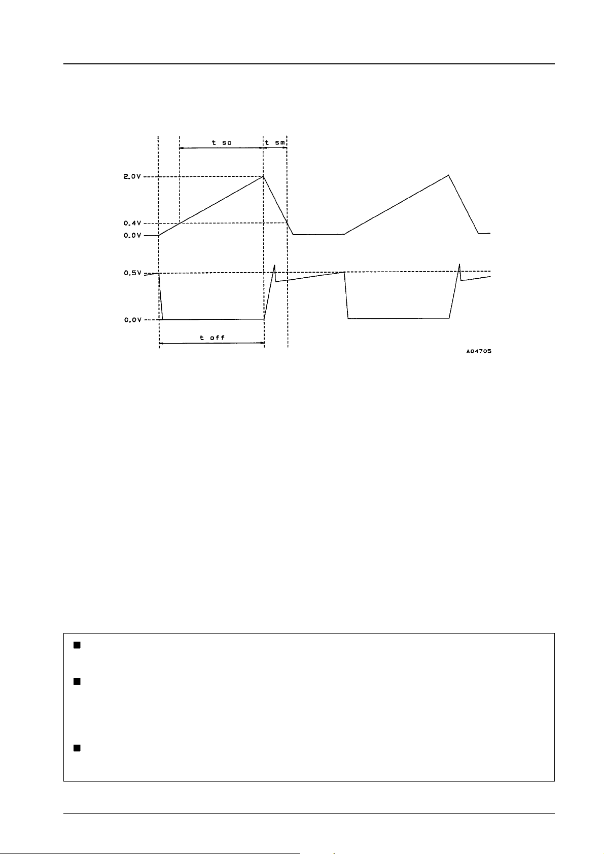
7-1. Output off time
The current limiter is so designed that current limit function turns on to turn off the sink side output transistor and then turn
on the transistor again after off period of a fixed time (output off time) has elapsed. Since the LB1694N uses this output
switching method for the current limiter, it is hardly necessary to consider ASO in current limiter operated mode as compared
with the output unsaturated current limited one. The output off time depends on charge time of capacitor C connected to the
C pin. When the current limiter turns on, C begins charging and the output is kept off until C is charged up to 2 V (typ).
When C has been charged up to 2 V, the sink side output turns on again. The C charging current is a constant-regulated
current which depends on resistor R connected to the R pin. The C charging current I
as follows:
I
6 1.3/R (R must be set to be 13 kΩ and 100 kΩ.)
CL
t
6 C/ICL× 2.0
off
6 1.53 × R × C
7-2. Output current neglect time
While the current limiter turns on and the sink side output is off, the regeneration current flows through the external diode
used for absorbing the regeneration current above the output that was turned off. After the output off time elapses and the
sink side output is turned on again, reverse current flows momentarily through the external diode (for the diode’s reverse
recovery time), causing the current that reaches the limiter value to flow momentarily through the output. Because this current
will cause current limiter to turn on again, turning off the output, the average current decreases, causing the torque to be
decreased at motor start-up, etc. Therefore, in order to prevent this current from being detected, the current limiter is designed
so that the output current is not detected for a fixed period of time after the sink side output is turned on again. This length
of time is the output current neglect time. The output current neglect time is determined by the discharge time of the
capacitor C connected to the C pin. When current limiter turns on and C charges to 2 V, C begins discharging, and the output
current neglect time is the time it takes for C to discharge to the point where the voltage at C is 0.4 V (typ). The C discharge
current is a constant current, and is set at about 3 times charge current I
about 1/3 of the output off time. The C discharge current I
and the output current neglect time tsmare determined
CH
, As a result, the output current neglect time is
CL
according to the following equations:
and output off time t
CL
are calculated
off
I
6 1.3/R × 3
CL
t
6 C/ICL× 1.6
sm
6 0.41 × R × C
Because there is a slope to the time at which the sink side output is turned on again, the reverse current is not very large,
even if a rectifier diode (a diode in which the reverse recovery time is not short) is used as the external diode for absorbing
the regeneration current in the current limiter.
7-3. Output off time setting
It is necessary to set the output off time to a suitable level for the type of motor being used. (The output off time is set by
the external resistors connected to the R pin, and by the external capacitor connected to the C pin.) Fig. 1 shows the current
limiter operation waveform.
(1) When the output off time is set short
The output current neglect time is set by a circuit within the IC to about 1/3 of the output off time. Therefore, if the
output off time is set to a very short length of time, the output current neglect time may not be adequate. If the output
current neglect time is inadequate, the current limiter will turn on in response to reverse current from the external diode
used to absorb the regeneration current. (Refer to Section 7-2.) Furthermore, if the output off time is short, the diode
reverse current becomes large and ASO must be considered.
No.5243-7/8
Page 8
LB1694N
(2) When the output off time is set long
If the output off time is set to a very long length of time, the average current decreases, with the result that the torque at
motor start-up drops. Depending on the type of motor, it may be impossible to shift from the current limiter operation
state to the normal rotation state.
C pin voltage
RF pin voltage
Fig. 1 Current Limiter Operation Waveform
8. Calculation of the IC’s internal power dissipation
Pd=(V
× ICC)+(VM×IM) – (power dissipated by the motor coil)
CC
9. Measuring the increase in the IC’s temperature
Because the temperature of the IC chip cannot be measured directly, the temperature is normally measured using one of the
following methods.
9-1. Measurement using a thermocouple
In order to measure the temperature by using a thermocouple, mount the thermocouple on the fin. Although this method of
measurement is simple, if the rate of heat generation has not stabilized, the measurement error is great.
9-2. Measurement using the characteristics of a diode within the IC
It is recommended that the parasitic diode between FG1 and GND be used to measure the temperature of the IC.
Set FG1 high (the ‘‘off’’ state), measure the parasitic diode voltage V
temperature characteristics of the voltage V
(Sanyo’s data: I
No products described or contained herein are intended for use in surgical implants, life-support systems, aerospace equipment,
nuclear power control systems, vehicles, disaster/crime-prevention equipment and the like, the failure of which may directly or
indirectly cause injury, death or property loss.
Anyone purchasing any products described or contained herein for an above-mentioned use shall:
1 Accept full responsibility and indemnify and defend SANYO ELECTRIC CO., LTD., its affiliates, subsidiaries and distributors
and all their officers and employees, jointly and severally, against any and all claims and litigation and all damages, cost and
expenses associated with such use:
2 Not impose any responsibility for any fault or negligence which may be cited in any such claim or litigation on SANYO
ELECTRIC CO., LTD., its affiliates, subsidiaries and distributors or any of their officers and employees jointly or severally.
Information (including circuit diagrams and circuit parameters) herein is for example only; it is not guaranteed for volume
production. SANYO believes information herein is accurate and reliable, but no guarantees are made or implied regarding its use
or any infringements of intellectual property rights or other rights of third parties.
= –1 mA, VFtemperature characteristics: approximately –2 mV/°C)
F
.
F
, and calculate the temperature based on the
F
This catalog provides information as of December, 1995. Specifications and information herein are subject to change without notice.
No.5243-8/8
 Loading...