


 R P2L97-S
Pentium® II Motherboard
USER’S MANUAL

USER'S NOTICE
No part of this manual, including the products and software described in it, may be reproduced, transmitted, transcribed, stored in a retrieval system, or translated into any language in any form or by any means, except documentation kept by the purchaser for backup purposes, without the express written permission of ASUSTeK COMPUTER INC. (“ASUS”).
ASUS PROVIDES THIS MANUAL “AS IS” WITHOUT WARRANTY OF ANY KIND, EITHER EXPRESS OR IMPLIED, INCLUDING BUT NOT LIMITED TO THE IMPLIED WARRANTIES OR CONDITIONS OF MERCHANTABILITY OR FITNESS FOR A PARTICULAR PURPOSE. IN NO EVENT SHALL ASUS, ITS DIRECTORS, OFFICERS, EMPLOYEES OR AGENTS BE LIABLE FOR ANY INDIRECT, SPECIAL, INCIDENTAL, OR CONSEQUENTIAL DAMAGES (INCLUDING DAMAGES FOR LOSS OF PROFITS, LOSS OF BUSINESS, LOSS OF USE OR DATA, INTERRUPTION OF BUSINESS AND THE LIKE), EVEN IF ASUS HAS BEEN ADVISED OF THE POSSIBILITY OF SUCH DAMAGES ARISING FROM ANY DEFECT OR ERROR IN THIS MANUAL OR PRODUCT.
Product warranty or service will not be extended if: (1) the product is repaired, modified or altered, unless such repair, modification of alteration is authorized in writing by ASUS; or (2) the serial number of the product is defaced or missing.
Products and corporate names appearing in this manual may or may not be registered trademarks or copyrights of their respective companies, and are used only for identification or explanation and to the owners’ benefit, without intent to infringe.
•Intel, LANDesk, and Pentium are registered trademarks of Intel Corporation.
•IBM and OS/2 are registered trademarks of International Business Machines.
•Symbios is a registered trademark of Symbios Logic Corporation.
•Windows and MS-DOS are registered trademarks of Microsoft Corporation.
•Sound Blaster AWE32 and SB16 are trademarks of Creative Technology Ltd.
•Adobe and Acrobat are registered trademarks of Adobe Systems Incorporated.
The product name and revision number are both printed on the product itself. Manual revisions are released for each product design represented by the digit before and after the period of the manual revision number. Manual updates are represented by the third digit in the manual revision number.
For previous or updated manuals, BIOS, drivers, or product release information, contact ASUS at http://www.asus.com.tw or through any of the means indicated on the following page.
SPECIFICATIONS AND INFORMATION CONTAINED IN THIS MANUAL ARE FURNISHED FOR INFORMATIONAL USE ONLY, AND ARE SUBJECT TO CHANGE AT ANY TIME WITHOUT NOTICE, AND SHOULD NOT BE CONSTRUED AS A COMMITMENT BY ASUS. ASUS ASSUMES NO RESPONSIBILITY OR LIABILITY FOR ANY ERRORS OR INACCURACIES THAT MAYAPPEAR IN THIS MANUAL, INCLUDING THE PRODUCTS AND SOFTWARE DESCRIBED IN IT.
Copyright © 1998 ASUSTeK COMPUTER INC. All Rights Reserved.
Product Name: |
ASUS P2L97-S |
Manual Revision: |
2.01 |
Release Date: |
April 1998 |
|
|
2 |
ASUS P2L97-S User’s Manual |

ASUS CONTACT INFORMATION
ASUSTeK COMPUTER INC.
Marketing
Address: |
150 Li-Te Road, Peitou, Taipei, Taiwan 112 |
Telephone: |
+886-2-2894-3447 |
Fax: |
+886-2-2894-3449 |
Email: |
info@asus.com.tw |
Technical Support
Fax: +886-2-2895-9254
BBS: +886-2-2896-4667
Email: tsd@asus.com.tw
WWW:www.asus.com.tw
FTP: ftp.asus.com.tw/pub/ASUS
ASUS COMPUTER INTERNATIONAL
Marketing
Address: |
6737 Mowry Ave, Mowry Business Center, Building 2, |
|
Newark, CA 94560, USA |
Fax: |
+1-510-608-4555 |
Email: |
info-usa@asus.com.tw |
Technical Support
Fax: +1-510-608-4555
BBS: +1-510-739-3774
Email: tsd-usa@asus.com.tw
WWW:www.asus.com
FTP: ftp.asus.com.tw/pub/ASUS
ASUS COMPUTER GmbH
Marketing
Address: |
Harkort Str. 25, 40880 Ratingen, BRD, Germany |
Telephone: |
49-2102-445011 |
Fax: |
49-2102-442066 |
Email: |
info-ger@asus.com.tw |
Technical Support
Hotline: 49-2102-499712
BBS: 49-2102-448690
Email: tsd-ger@asus.com.tw
WWW:www.asuscom.de
FTP: ftp.asuscom.de/pub/ASUSCOM
ASUS P2L97-S User’s Manual |
3 |

CONTENTS
I. INTRODUCTION |
7 |
How this Manual is Organized ........................................................... |
7 |
Item Checklist ..................................................................................... |
7 |
II. FEATURES |
8 |
Features of the ASUS P2L97-S Motherboard ..................................... |
8 |
The ASUS P2L97-S Motherboard ................................................ |
9 |
III. INSTALLATION |
10 |
Layout of the ASUS P2L97-S Motherboard ..................................... |
10 |
Installation Steps ............................................................................... |
12 |
1. Jumpers ......................................................................................... |
12 |
Jumper Settings ..................................................................... |
13 |
2. System Memory (DIMM) ............................................................ |
17 |
DIMM Memory Installation Procedures: .............................. |
18 |
3. Central Processing Unit (CPU) .................................................... |
19 |
Pentium II Processor .............................................................. |
19 |
AAVID Heatsink ................................................................... |
23 |
Elan Vital Heatsink ................................................................ |
23 |
4. Expansion Cards ........................................................................... |
24 |
Expansion Card Installation Procedure ................................. |
24 |
Assigning IRQs for Expansion Cards .................................... |
24 |
Assigning DMA Channels for ISA Cards .............................. |
25 |
ISA Cards and Hardware Monitor ......................................... |
25 |
Accelerated Graphics Port ..................................................... |
25 |
5. External Connectors ..................................................................... |
26 |
Power Connection Procedures .................................................... |
33 |
IV. BIOS SOFTWARE |
34 |
Support Software ......................................................................... |
34 |
Flash Memory Writer Utility ....................................................... |
34 |
Main Menu ............................................................................ |
35 |
Advanced Features Menu ...................................................... |
35 |
Managing & Updating your Motherboard’s BIOS ...................... |
36 |
6. BIOS Setup .................................................................................. |
37 |
Load Defaults ........................................................................ |
38 |
Standard CMOS Setup ................................................................ |
38 |
Details of Standard CMOS Setup: ......................................... |
38 |
BIOS Features Setup ................................................................... |
41 |
Details of BIOS Features Setup ............................................. |
41 |
4 |
ASUS P2L97-S User’s Manual |

CONTENTS
Chipset Features Setup ................................................................ |
44 |
Details of Chipset Features Setup .......................................... |
44 |
Power Management Setup ........................................................... |
47 |
Details of Power Management Setup .................................... |
47 |
PNP and PCI Setup ..................................................................... |
50 |
Details of PNP and PCI Setup ............................................... |
50 |
Load BIOS Defaults .................................................................... |
52 |
Load Setup Defaults .................................................................... |
52 |
Supervisor Password and User Password ................................... |
53 |
IDE HDD Auto Detection ........................................................... |
54 |
Save & Exit Setup ....................................................................... |
55 |
Exit Without Saving .................................................................... |
55 |
V. DESKTOP MANAGEMENT |
56 |
Desktop Management Interface (DMI) ............................................. |
56 |
Introducing the ASUS DMI Configuration Utility ................ |
56 |
System Requirements ............................................................ |
56 |
Using the ASUS DMI Configuration Utility ......................... |
57 |
VI. ADAPTEC SCSI SELECT |
59 |
Configuring the SCSI Adapter .......................................................... |
59 |
Configure/View Host Adapter Settings ................................. |
59 |
SCSI Disk Utilities ...................................................................... |
59 |
VII. ADAPTEC EZ-SCSI UTILITY |
61 |
Quick Start Instructions .................................................................... |
61 |
Windows95 or WindowsNT ........................................................ |
61 |
Windows/Windows for Workgroups 3.1x ................................... |
61 |
DOS ............................................................................................. |
61 |
Troubleshooting Tips ........................................................................ |
62 |
SCSI Device Troubleshooting ..................................................... |
62 |
Windows95/WindowsNT Troubleshooting ................................. |
62 |
Information for DOS/Windows 3.1x Users ...................................... |
65 |
DOS and Windows3.1x Device Drivers ...................................... |
65 |
DOS and Windows3.1x ASPI Managers ..................................... |
65 |
DOS Formatting Utilities ............................................................ |
66 |
Low-level Formatter (scsifmt) ............................................... |
66 |
Formatter and Partitioner (afdisk) ......................................... |
67 |
VIII. ADAPTEC 7800 FAMILY MANAGER SET (84 pages) |
|
(Drivers for onboard Adaptec 7880 SCSI Chipset) |
|
ASUS P2L97-S User’s Manual |
5 |

FCC & DOC COMPLIANCE
Federal Communications Commission Statement
This device complies with FCC Rules Part 15. Operation is subject to the following two conditions:
•This device may not cause harmful interference, and
•This device must accept any interference received, including interference that may cause undesired operation.
This equipment has been tested and found to comply with the limits for a Class B digital device, pursuant to Part 15 of the FCC Rules. These limits are designed to provide reasonable protection against harmful interference in a residential installation. This equipment generates, uses and can radiate radio frequency energy and, if not installed and used in accordance with manufacturer's instructions, may cause harmful interference to radio communications. However, there is no guarantee that interference will not occur in a particular installation. If this equipment does cause harmful interference to radio or television reception, which can be determined by turning the equipment off and on, the user is encouraged to try to correct the interference by one or more of the following measures:
•Re-orient or relocate the receiving antenna.
•Increase the separation between the equipment and receiver.
•Connect the equipment to an outlet on a circuit different from that to which the receiver is connected.
•Consult the dealer or an experienced radio/TV technician for help.
WARNING! The use of shielded cables for connection of the monitor to the graphics card is required to assure compliance with FCC regulations. Changes or modifications to this unit not expressly approved by the party responsible for compliance could void the user's authority to operate this equipment.
Canadian Department of Communications Statement
This digital apparatus does not exceed the Class B limits for radio noise emissions from digital apparatus set out in the Radio Interference Regulations of the Canadian Department of Communications.
6 |
ASUS P2L97-S User’s Manual |

I. INTRODUCTION
How this Manual is Organized
This manual is divided into the following sections:
I. |
Introduction |
Manual information and checklist |
II. |
Features |
Information and specifications |
III. |
Installation |
Instructions on setting up the motherboard. |
IV. |
BIOS Software |
Instructions on setting up the BIOS software |
V. |
DMI Utility |
BIOS supported Desktop Management Interface |
VI. |
Adaptec SCSI Select |
Adaptec SCSI Select utility |
VII. Adaptec EZ-SCSI |
Adaptec EZ-SCSI utility |
|
VIII. Adaptec 7800 |
Adaptec SCSI driver installation and usage |
|
Item Checklist
Check that your package is complete. If you discover damaged or missing items, contact your retailer.
ASUS P2L97-S motherboard
Retention mechanism & heatsink support
1 IDE ribbon cable
1 floppy ribbon cable
50-pin Fast SCSI cable
ASUS P2L97-S Support Drivers & Utilities
•Flash Memory Writer utility to update the FLASH BIOS
•Desktop Management Interface (DMI) utility
•LANDesk® Client Manager (LDCM) Software (with optional onboard LM78)
•Adaptec SCSI drivers and utilities
•Readme files for descriptions and use of the files
•Technical Support Form
This user’s manual
Infrared module (optional)
68-Pin Fast&Wide-SCSI cable (optional)
I. INTRODUCTION |
(Manual / Checklist) |
|
|
ASUS P2L97-S User’s Manual |
7 |

FEATURES .II (Specifications)
II. FEATURES
Features of the ASUS P2L97-S Motherboard
The ASUS P2L97-S is carefully designed for the demanding PC user who wants many features processed by the fastest CPU. This motherboard:
•Versatile Processor Support: Intel Pentium® II (233MHz–333MHz) processor.
•Intel Chipset: Features Intel’s 440LX AGPset with I/O subsystems.
•Adaptec SCSI Chipset: Features Adaptec’s 7880 Ultra-Fast/Wide SCSI chipset.
•Easy Installation: Equipped with BIOS that supports auto detection of hard drives, PS/2 mouse, and Plug and Play devices to make setup of hard drives, expansion cards, and other devices virtually automatic.
•ISA & PCI Expansion Slots: Provides one 16-bit ISA, three 32-bit PCI slots, and one ISA/PCI shared slot.
•Super Multi-I/O: Provides two high-speed UART compatible serial ports and one parallel port with EPP and ECP capabilities. UART2 can also be directed from COM2 to the Infrared Module for wireless connections.
•Desktop Management Interface (DMI): Supports DMI through BIOS, which allows hardware to communicate within a standard protocol creating a higher level of compatibility. (Requires DMI-enabled components.) (See section V)
•PCI Bus Master IDE Controller: Comes with an onboard PCI Bus Master IDE controller with two connectors that supports four IDE devices in two channels, supports PIO Modes 3 and 4 and Bus Master IDE DMA Mode 2, and supports Enhanced IDE devices, such as Tape Backup and CD-ROM drives. Two floppy drives of either 5.25inch or 3.5inch (1.44MB or 2.88MB) are also supported without an external card. Supports Japanese standard “Floppy 3 mode” (3.5-inch disk drive: 1.2MB) and LS-120 floppy disk drives (3.5-inch disk drive: 120 MB, 1.44MB, 720K). BIOS supports IDE CD-ROM or SCSI device boot-up.
•Multi-Cache: Supports a Pentium® II processor with either 512KB, 256KB, or 0KB Pipelined Burst Level 2 cache in the Single Edge Contact (SEC) cartridge.
•Versatile Memory Support: Equipped with three DIMM sockets to support (8, 16, 32, 64, or 128MB) 168-pin SDRAM/EDO memory modules up to 384MB.
•IrDA: Supports an optional infrared port module for wireless interface.
•Concurrent PCI: Concurrent PCI allows multiple PCI transfers from PCI master busses to memory to CPU.
•AGP: Supports Accelerated Graphics Port cards for high performance, component level interconnect targeted at 3D graphical display applications.
•Intelligence: Supports Fan Status Monitoring and Alarm, Temperature Monitoring and Alert, Voltage Monitoring and Alert, System Resources Alert, and Virus Write Protection through the optional onboard LM78 Hardware Monitor and Intel® LANDesk Client Manager (LDCM) software.
8 |
ASUS P2L97-S User’s Manual |

II. FEATURES
The ASUS P2L97-S Motherboard
|
|
|
|
|
|
|
|
|
|
|
|
|
|
|
|
|
|
|
|
|
|
|
|
Adaptec’s 7880 |
||
|
|
|
|
|
|
|
|
|
|
|
|
|
|
|
|
|
|
|
|
|
|
|
|
Ultra-Fast/Wide |
||
|
|
|
|
|
|
|
|
|
|
|
|
|
|
|
|
|
|
|
|
|
Intel 440LX AGPset Narrow/Wide SCSI Connectors |
SCSI Chipset |
||||
|
|
|
|
|
|
|
|
|
|
|
|
|
|
|
|
|||||||||||
|
|
|
|
|
|
|
|
|
|
|
|
|
|
|
|
|
||||||||||
|
|
|
|
|
|
|
|
|
|
|
|
|
|
|
|
|
|
|
|
|
|
|
|
|
|
|
PS/2 Mouse (Top) |
|
|
|
|||||||||||||||||||||||
|
|
|
||||||||||||||||||||||||
|
|
|
||||||||||||||||||||||||
PS/2 K’board (Bottom) |
|
|
|
|||||||||||||||||||||||
USB Port 1 (Top) |
|
|
|
|
|
|||||||||||||||||||||
USB Port 2 (Bottom) |
|
|
|
|||||||||||||||||||||||
COM 1 |
|
|
|
|
|
|
|
|
|
|
||||||||||||||||
|
|
|
|
|
||||||||||||||||||||||
(Bottom) |
|
|
|
|||||||||||||||||||||||
Parallel (Top) |
|
|
|
|||||||||||||||||||||||
Serial (Bottom) |
|
|
|
|
|
|
|
|
|
|
|
|
|
|||||||||||||
COM 2 |
|
|
|
|
|
|
|
|
|
|
|
|
|
|
|
|
|
|
|
|
|
|
|
|
|
|
(Bottom) |
|
|
|
|||||||||||||||||||||||
SEC CPU Slot |
|
|
|
|
|
|
|
|
|
|||||||||||||||||
|
|
|
|
|
|
|||||||||||||||||||||
Floppy Disk Drive |
|
|
|
|||||||||||||||||||||||
Connector |
|
|
|
|
|
|
|
|
|
|
|
|||||||||||||||
3 DIMM |
|
|
|
|
|
|
||||||||||||||||||||
|
|
|
|
|||||||||||||||||||||||
Sockets |
|
|
|
|||||||||||||||||||||||
Accelerated |
|
|
|
|||||||||||||||||||||||
Graphics Port |
|
|
|
|
|
|
|
|
|
|
|
|
|
|
|
|
||||||||||
|
|
|
|
|
|
|
|
|
|
|||||||||||||||||
Multi-I/O |
|
|
|
|
|
|
|
|
|
|
|
|
|
|||||||||||||
|
|
|
|
|
|
|
|
|||||||||||||||||||
3 PCI Slots |
|
|
|
|
|
|
|
|
|
|
|
|
|
|
|
|
|
|
|
|||||||
|
|
|
|
|
|
|
|
|
|
|
|
|
|
|||||||||||||
Hardware |
|
|
|
|||||||||||||||||||||||
Monitor |
|
|
|
|
|
|
|
|
|
|
|
|
||||||||||||||
Programmable |
|
|
|
|
|
|||||||||||||||||||||
2MB Flash ROM |
|
|
|
|||||||||||||||||||||||
1 ISA/PCI |
|
|
|
|
|
|||||||||||||||||||||
Shared Slot |
|
|
|
|||||||||||||||||||||||
1 ISA Slot
Intel PIIX4 PCIset
II. FEATURES (Motherboard Parts)
ASUS P2L97-S User’s Manual |
9 |
INSTALLATION .III Layout) (Board
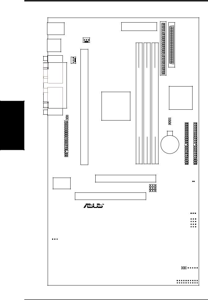
III. INSTALLATION
Layout of the ASUS P2L97-S Motherboard
|
|
Mouse (top port) |
ATX Power Connector |
34 68 |
|
|
|||
PS/2 |
|
|
|
|
|
||||
|
Keyboard (bottom port) |
|
|
|
|
|
|
|
|
|
|
|
|
|
|
SCSI |
|
|
|
|
|
PWR_FAN |
|
|
|
|
|
|
|
|
|
|
|
|
|
Pin-Wide |
|
|
|
|
|
CPU_FAN |
|
|
|
|
|
|
|
USB |
USB 1 (top port) |
|
|
|
|
|
|
|
|
|
USB 2 (bottom port) |
|
|
|
|
|
|
|
|
COM 1 |
|
|
|
|
|
|
68 |
|
|
|
|
|
|
|
|
|
|
|
|
|
DrivesDiskFloppy |
CPUContactEdgeSingleSlot |
168bit,(643Socket(DIMMpin module) |
168bit,(642Socket(DIMMpin module) |
168bit,(641Socket(DIMMpin module) |
35 |
1 |
IDESecondary |
IDEPrimary |
ParallelPort |
SCSIConnector |
|
|||||||
|
|
|
|
|
Adaptec |
|
|||
|
|
|
|
|
|
|
7880 SCSI |
||
|
|
|
Intel |
|
|
Pin |
Chipset |
|
|
|
|
|
440LX |
|
|
|
|
|
|
COM 2 |
|
|
AGPset |
|
|
50- |
|
|
|
|
|
R_CPU |
|
|
|
SCSI |
|
|
|
|
|
|
|
|
|
|
|
|
|
|
|
|
|
|
|
BIOS Power |
|
|
|
|
|
|
|
|
|
(CR2032 3V |
|
|
|
|
|
|
|
|
|
Lithium Cell) |
|
|
|
Multi-I/O |
Accelerated Graphics Port |
|
|
|
|
CLRTC |
|||
|
|
|
FS0 |
|
|
|
|||
|
|
|
|
|
|
|
|
|
|
|
|
|
|
|
|
FS1 |
|
|
|
|
|
|
|
|
|
FS2 |
|
|
|
|
|
|
PCI Slot 1 |
BUS FREQ |
|
|
|
||
|
|
|
|
|
|
|
|
|
|
|
|
Hardware |
|
|
|
|
|
|
R |
|||||||||||||||||||
|
|
|
|
|
|
|||||||||||||||||||||||
|
|
|
Monitor |
|
|
|
|
|
|
|
|
|
|
|
|
|
|
|
CHA_FAN |
|||||||||
|
|
|
|
|
|
|
|
|
|
|
|
|
|
|
||||||||||||||
|
|
|
|
|
|
|
|
|
|
|
|
|
|
|
|
|
|
|
|
|
|
|
|
|||||
|
|
|
LM78 |
|
|
|
|
|
|
|
PCI Slot 2 |
|
|
|
|
|
|
|
|
|
|
|
|
|||||
|
|
|
|
|
|
|
|
|
|
|
|
|
|
|
|
|
|
|
|
|
|
|||||||
|
|
|
|
|
|
|
|
|
|
|
|
|
|
|
|
|
|
|
|
|
|
|
|
|
|
|
|
|
|
|
|
|
|
|
|
|
|
|
|
|
|
|
|
|
|
|
|
|
FREQ BF0 |
|
|||||||
|
|
|
|
|
|
|
|
|
EEPROMFlash2MB |
BIOS)(Programable |
|
|
|
|
|
|
|
|
|
RATIO BF1 |
|
|||||||
|
|
|
|
|
|
|
|
|
|
|
|
|
|
|
|
|
|
|
|
|
|
BF2 |
|
|
|
|||
|
|
|
|
|
|
|
|
|
|
|
|
|
|
|
|
|
|
|
|
|
|
|
|
BF3 |
|
|||
WOL_CON |
|
|
|
|
|
|
|
|
PCI Slot 3 |
|
|
|
|
|
|
|
|
|
|
|
|
|||||||
|
|
|
|
|
|
|
|
Intel PIIX4 |
|
|
|
|
|
|
|
|
||||||||||||
|
|
|
|
|
|
|
|
|
|
|
|
|
|
|
|
|
|
|
||||||||||
|
|
|
|
|
|
|
|
|
|
|
|
|
|
|
|
|
|
|
||||||||||
|
|
|
|
|
|
|
|
|
|
|
|
|
|
|
|
|
|
|
|
|
|
|
|
|
|
|||
|
|
|
|
|
|
|
|
|
|
|
|
|
|
|
|
|
|
|
|
|
|
|
|
|
|
|||
|
|
|
|
|
|
|
|
|
|
|
|
|
|
|
|
|
|
|
|
|
|
|
|
|
|
|||
|
R_MB1 |
|
|
|
|
|
|
|
|
|
|
|
PCIset |
|
|
|
|
|
|
|
|
|||||||
|
|
|
|
|
|
|
|
|
PCI Slot 4 |
|
|
|
|
|
|
|
|
|
|
|
|
|||||||
|
|
|
|
|
|
|
|
|
|
|
|
|
|
|
|
|
|
|
|
|
|
|
|
|
|
|
||
|
|
Thermal |
|
|
|
|
|
|
|
|
|
|
|
|
|
|
|
|
|
|
|
|
|
|
|
|||
|
|
|
|
|
|
|
|
|
|
|
|
|
|
|
|
|
|
|
|
|||||||||
|
Sensor |
|
|
|
|
|
|
|
|
|
|
|
|
|
|
|
|
|
|
|
|
|
|
|||||
|
|
|
|
|
|
|
|
|
|
|
|
|
|
|
|
|
|
|
|
|
|
|||||||
|
|
|
|
|
|
|
|
|
|
|
|
|
|
|
|
ISA Slot 1 |
|
|
|
|
|
|
|
|
|
|
||
|
|
|
|
|
|
|
|
|
|
|
|
|
|
|
|
|
|
|
|
|
|
|
|
|
||||
|
|
|
|
|
|
|
|
|
|
|
|
|
|
|
|
|
|
|
|
|
|
|
|
|
|
|
|
|
|
|
|
|
|
|
|
|
|
|
|
|
|
|
|
|
|
|
|
|
HDLED IrDA |
||||||||
|
|
|
|
|
|
|
|
|
|
|
|
|
|
|
|
|
|
|
|
Panel Connect. |
||||||||
|
|
|
|
|
|
|
|
|
|
|
|
|
|
|
|
ISA Slot 2 |
|
|||||||||||
|
|
|
|
|
|
|
|
|
|
|
|
|
|
|
|
|
|
|
|
|
|
|
|
|
|
|||
|
|
|
|
|
|
|
|
|
|
|
|
|
|
|
|
|
|
|
|
|
|
|||||||
|
|
|
|
|
|
|
|
|
|
|
|
|
|
|
|
|
|
|
|
|
|
|
|
|
|
|
|
|
10 |
ASUS P2L97-S User’s Manual |
III. INSTALLATION
Jumpers
1) |
SCSI |
p. 13 |
Onboard SCSI Setting |
2) |
FS0, FS1, FS2 |
p. 14 |
CPU Bus Frequency |
3) |
BF0, BF1, BF2, BF3 |
p. 14 |
CPU Core:Bus Frequency Multiple |
4) |
CLRTC |
p. 15 Clear Real Time Clock (RTC) RAM |
|
Expansion Slots/Sockets
1) |
System Memory |
p. 17 System Memory Support |
|
2) |
DIMM Sockets |
p. 18 DIMM Memory Module Support |
|
3) |
SEC CPU Slot |
p. 19 |
Single Edge Contact CPU Support |
4) |
SLOT1, SLOT2 |
p. 24 |
16-bit ISA Bus Expansion Slots* |
5) |
PCI1, PCI2, PCI3, PCI4 |
p. 25 |
32-bit PCI Bus Expansion Slots† |
6) |
AGP |
p. 25 |
Accelerated Graphics Port |
Hardware Monitor
1) R_CPU p. 22 Pentium II Processor Thermal Sensor Connector
Connectors
1) |
PS2KEYBOARD |
p. 26 PS/2 Keyboard Connector (6-pin female) |
|
2) |
PS2MOUSE |
p. 26 PS/2 Mouse Connector (6-pin female) |
|
3) |
PRINTER |
p. 27 |
Parallel (Printer) Port Connector (25-pin female) |
4) |
COM1, COM2 |
p. 27 Serial Port COM1 & COM2 (two 9-pin male) |
|
5) |
FLOPPY |
p. 27 |
Floppy Drive Connector (34-1 pin block) |
6) |
USB |
p. 28 |
Universal Serial BUS Ports 1 & 2 (two 4-pin female) |
7) |
Primary / Second IDE |
p. 28 Primary / Secondary IDE Connector (40-pin blocks) |
|
8) |
HDLED |
p. 29 IDE LED Activity Light (2 pins) |
|
9) |
CHA_, CPU_, PWR_FAN |
p. 29 |
Chassis, CPU, Power Supply Fan Connectors (3-pin block) |
10) |
IR |
p. 30 |
Infrared Port Module Connector (5 pins) |
11) |
ATXPWR |
p. 30 ATX Motherboard Power Connector (20-pin block) |
|
12) |
WOL |
p. 31 Wake on LAN (3 pins) (Reserved) |
|
13) NARROW/WIDE SCSI |
p. 31 |
50-pin Fast SCSI II & 68-pin Fast&Wide SCSI III |
|
14) TB_LED (PANEL) |
p. 32 LED Lead (2 pins) |
||
15) |
SMI (PANEL) |
p. 32 SMI Switch Switch Lead (2 pins) |
|
16) PWR_SW (PANEL) |
p. 32 |
ATX Power Switch / Soft Power Switch (2 pins) |
|
17) |
RESET (PANEL) |
p. 32 Reset Switch Lead (2 pins) |
|
18) KEYLOCK (PANEL) |
p. 32 |
System Power LED (3 pins) |
|
19) KEYLOCK (PANEL) |
p. 32 |
Keyboard Lock Switch Lead (2 pins) |
|
20) |
SPEAKER (PANEL) |
p. 32 Speaker Connector (4 pins) |
|
*The onboard hardware monitor uses the address 290H-297H so legacy ISA cards must not use this address or else conflicts will occur.
† PCI slots 4 share the same interrupt number (INT#) as the onboard SCSI so PCI slot 4 card must be able to share an INT# or make sure that it does not use an INT# at all.
III. INSTALLATION (Board Layout)
ASUS P2L97-S User’s Manual |
11 |
INSTALLATION .III (Jumpers)
III. INSTALLATION
Installation Steps
Before using your computer, you must complete the following steps:
1.Set Jumpers
2.Install Memory Modules
3.Install the Central Processing Unit (CPU)
4.Install Expansion Cards
5.Connect Ribbon Cables, Cabinet Wires, and Power Supply
6.Setup the BIOS Software
1. Jumpers
Several hardware settings are made through the use of jumper caps to connect jumper pins (JP) on the motherboard. See motherboard layout on page 10 for locations of jumpers. The jumper settings will be described numerically such as [----], [1-2], [2-3] for no connection, connect pins 1&2, and connect pins 2&3 respectively. Pin 1
PIN 1

|
|
PIN 1 |
|
for our motherboards is always on top |
or on the left |
|
when holding the |
|
|||
|
|||
motherboard with the keyboard connector away from yourself. A “1” is written besides pin 1 on jumpers with three pins. The jumpers will also be shown graphi-
cally such as |
|
to connect pins 1&2 and |
|
to connect pins 2&3. Jumpers |
|||
|
|
||||||
with two pins will be shown as |
|
for Short (On) and |
for Open (Off). For |
||||
|
|||||||
|
|||||||
manufacturing simplicity, the jumpers may be sharing pins from other groups. Use the diagrams in this manual instead of following the pin layout on the board. Settings with two jumper numbers require that both jumpers be moved together. To connect the pins, simply place a plastic jumper cap over the two pins as diagramed.
WARNING! Computer motherboards and expansion cards contain very delicate Integrated Circuit (IC) chips. To protect them against damage from static electricity, you should follow some precautions whenever you work on your computer.
1.Unplug your computer when working on the inside.
2.Use a grounded wrist strap before handling computer components. If you do not have one, touch both of your hands to a safely grounded object or to a metal object, such as the power supply case.
3.Hold components by the edges and try not to touch the IC chips, leads or connectors, or other components.
4.Place components on a grounded antistatic pad or on the bag that came with the component whenever the components are separated from the system.
12 |
ASUS P2L97-S User’s Manual |
III. INSTALLATION
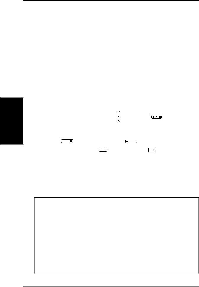
Jumper Settings
1.Onboard SCSI Setting (SCSI)
This motherboard gives you the option of using the onboard Adaptec 7880 SCSI BIOS through either the PnP and PCI Setup of the BIOS SOFTWARE or the use of jumper caps.
Selection |
SCSI |
Enable |
[1-2] |
Disable |
[2-3] |
P2L97-S SCSI Setting |
|
SCSI |
SCSI |
||||
1 |
2 |
3 |
1 |
2 |
3 |
|
|
|
|
||
Enable |
Disable |
||||
INSTALLATION |
(Jumpers) |
III. |
|
|
|
ASUS P2L97-S User’s Manual |
13 |

INSTALLATION .III (Jumpers)
III.INSTALLATION
2.CPU Bus Frequency (FS0, FS1, FS2)
This option tells the clock generator what frequency to send to the CPU. This allows the selection of the CPU’s External frequency (or BUS Clock). The BUS Clock multiplied by the BUS Ratio equals the CPU’s Internal frequency (the advertised CPU speed).
3.CPU Core:BUS Frequency Multiple (BF0, BF1, BF2, BF3)
This option sets the frequency ratio between the Internal frequency of the CPU and the CPU’s External frequency. These must be set in conjunction with the
CPU Bus Frequency.
FS2 FS1 FS0 |
FS2 FS1 FS0 |
FS2 FS1 FS0 |
FS2 FS1 FS0 |
|
1 |
1 |
1 |
1 |
|
2 |
2 |
2 |
2 |
|
3 |
3 |
3 |
3 |
60MHz |
66MHz |
75MHz |
|
83MHz |
CPU Bus Frequency
|
|
|
|
|
BF3 BF2 BF1 BF0 |
BF3 BF2 BF1 BF0 |
BF3 BF2 BF1 BF0 |
BF3 BF2 BF1 BF0 |
BF3 BF2 BF1 BF0 |
|
|
|
|
||||||
|
|
|
|
||||||
|
|
|
|
1 |
1 |
1 |
1 |
|
2 |
|
2 |
2 |
2 |
|
P2L97-S CPU Settings |
3 |
|
3 |
3 |
3 |
|
2.0x(2/1) |
3.5x(7/2) |
4.0x(4/1) |
4.5x(9/2) |
5.0x(5/1) |
||
|
CPU Core:Bus Frequency Multiple
WARNING! Frequencies above 66Mhz exceed the specifications for the onboard Intel Chipset and are not guaranteed to be stable.
Intel Pentium II Processor in a SEC Cartridge (233-333MHz 512KB/256KB/0KB L2 Cache)
Set the jumpers by the Internal speed of your processor as follows:
CPU Model |
Freq. |
|
|
|
|
|
(BUS Freq.) |
|
(Freq. |
|
Ratio) |
|
||
|
|
|
|
|
|
|
||||||||
|
|
|
|
|
|
|
|
|||||||
Ratio |
BUS F. |
FS2 |
FS1 |
FS0 |
BF3 |
BF2 |
BF1 |
BF0 |
||||||
Intel Pentium II |
333MHz |
5.0x |
66MHz |
[1-2] [1-2] [1-2] |
[2-3] |
[1-2] [1-2] [2-3] |
||||||||
Intel Pentium II |
300MHz |
4.5x |
66MHz |
[1-2] [1-2] [1-2] |
[2-3] |
[1-2] [2-3] [1-2] |
||||||||
Intel Pentium II |
266MHz |
4.0x |
66MHz |
[1-2] [1-2] [1-2] |
[2-3] |
[1-2] [2-3] [2-3] |
||||||||
Intel Pentium II |
233MHz |
3.5x |
66MHz |
[1-2] |
[1-2] |
[1-2] |
[2-3] |
[2-3] |
[1-2] |
[1-2] |
||||
IMPORTANT: Do not set the Frequency Ratio (BF) jumpers to all [2-3], this will cause unexpected behaviors.
NOTES: Overclocking your processor is not recommended. It may result in a slower speed. Voltage Regulator Output Selection (VID) is not needed for the Pentium II processor because it sends a VID signal directly to the onboard power controller.
14 |
ASUS P2L97-S User’s Manual |
III.INSTALLATION
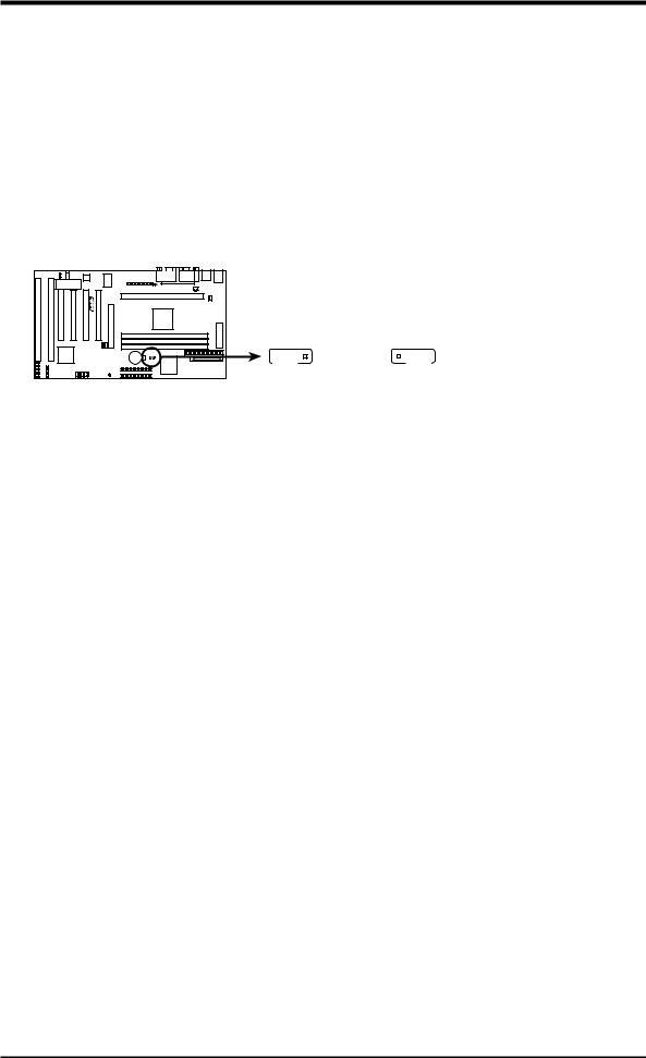
4.Real Time Clock (RTC) RAM (CLRTC)
The CMOS RAM is powered by the onboard button cell battery. To clear the RTC data: (1) Turn off your computer and unplug its AC power, (2) Short the two solder points labeled CLRTC, (3) Turn on your computer, (4) Hold down <Delete> during bootup and enter BIOS setup to re-enter user preferences.
Short the solder points to clear CMOS
CLRTC
P2L97-S Real Time Clock RAM (CLRTC)
INSTALLATION |
(Jumpers) |
III. |
|
|
|
ASUS P2L97-S User’s Manual |
15 |

(This page was intentionally left blank)
INSTALLATION .III (Jumpers)
16 |
ASUS P2L97-S User’s Manual |
III.INSTALLATION
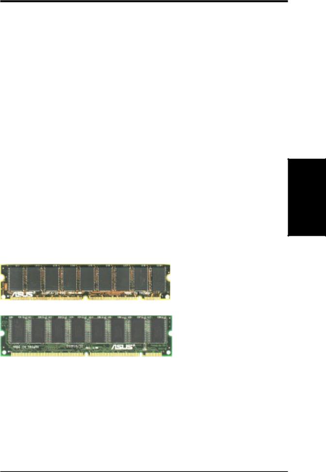
2.System Memory (DIMM)
Only Dual Inline Memory Modules (DIMM’s) can be used with this motherboard. Two sockets are available for 3.3Volt (power level) Unbuffered Synchronous DRAMs (SDRAM) or EDO DRAM of either 8, 16, 32, 64, or 128MB to form a memory size between 8MB to 384MB. One side (with memory chips) of the DIMM module takes up one Row on the motherboard.
To utilize the chipset’s Error Checking and Correction (ECC) feature, you must use a DIMM module with 9 chips per side (standard 8 chips/side + 1 parity chip) and make the proper settings in the BIOS Chipset Features Setup.
IMPORTANT: Memory speed setup is required through "Auto Configuration" in BIOS Chipset Features Setup.
Install memory in any combination as follows:
DIMM Location |
168-pin DIMM Memory Modules |
|
Total Memory |
Socket 1 (Rows 0&1) |
SDRAM/EDO 8, 16, 32, 64, 128MB |
x1 |
|
|
|
|
|
Socket 2 (Rows 2&3) |
SDRAM/EDO 8, 16, 32, 64, 128MB |
x1 |
|
|
|
|
|
Socket 3 (Rows 4&5) |
SDRAM/EDO 8, 16, 32, 64, 128MB |
x1 |
|
|
|
|
|
|
Total System Memory (Max 384MB) |
= |
|
|
|
|
|
ASUS Memory Examples:
Parity EDO DIMM (9 chips)
Non-Parity SDRAM DIMM (8 chips)
General DIMM Notes: (not true for all memory modules)
•Four possible memory chips are supported: EDO or SDRAM with and without parity.
•SDRAM chips are generally thinner with higher pin density than EDO chips.
•BIOS shows EDO or SDRAM memory on bootup screen.
•8 chip/side modules do not support parity, only 9 chip/side modules support parity.
•Single sided modules are usually 16 or 64 MB, double sided are usually 8, 32, or 128MB.
III. INSTALLATION (System Memory)
ASUS P2L97-S User’s Manual |
17 |

III. INSTALLATION
DIMM Memory Installation Procedures:
Insert the module(s) as shown. Because the number of pins are different on either side of the breaks, the module will only fit in the orientation as shown. DRAM SIMM modules have the same pin contact on both sides. SDRAM DIMM modules have a different pin contact on each side and therefore have a higher pin density.
INSTALLATION .III Memory) (System
|
|
|
|
|
|
|
|
|
|
|
|
|
|
|
|
|
|
|
|
|
|
|
|
|
|
|
|
|
|
|
|
|
|
|
|
|
|
|
|
|
|
|
|
|
|
|
|
|
|
|
|
|
|
|
|
|
|
|
|
|
|
|
|
|
|
|
|
|
|
|
|
|
|
|
|
|
|
|
|
|
|
|
|
|
|
|
|
|
|
|
|
|
|
|
|
|
|
|
|
|
|
|
|
|
|
|
|
|
|
|
|
|
|
|
|
|
|
|
|
|
|
|
|
|
|
|
|
|
|
|
|
|
|
|
|
|
|
|
|
|
|
|
|
|
|
|
|
|
|
|
|
|
|
|
|
|
|
|
|
|
|
|
|
|
|
|
|
|
|
|
|
|
|
|
|
|
|
|
|
|
|
|
|
|
|
|
|
|
|
|
|
|
|
|
|
|
|
|
|
|
|
|
|
|
|
|
|
|
|
|
|
20 Pins 60 Pins |
|
88 Pins |
|||||||
|
|
|
|
|
|
|
|
|
|
|
|
|
|
|
|
|
|
|
|
|
|
|
||||||||||||||
|
|
|
|
|
|
|
|
|
|
|
|
|
|
|
|
|
|
|
|
|
|
|
||||||||||||||
|
|
|
|
|
|
|
|
|
|
|
|
|
||||||||||||||||||||||||
|
|
|
|
|
|
|
|
|
|
|
|
|
|
|
|
|
|
|
|
|
|
|
|
|
|
|
|
|
|
|
|
|
|
|
|
|
|
|
|
|
|
|
|
|
|
|
|
|
|
|
|
|
|
|
|
|
|
|
|
|
|
|
|
|
|
|
|
|
|
|
|
|
|
|
|
|
|
|
|
|
|
|
|
|
|
|
|
|
|
|
|
|
|
|
|
|
|
|
|
|
|
|
|
|
|
|
|
|
|
|
|
|
|
|
|
|
|
|
|
|
|
|
|
|
|
|
|
|
|
|
|
|
|
|
|
|
|
|
|
|
|
|
|
|
|
|
|
Lock
(FRONT)
P2L97-S 168-Pin DIMM Memory Sockets
The Dual Inline Memory Module (DIMM) memory modules must be 3.3Volt Unbuffered Synchronous DRAM (SDRAM) or Extended Data Output (EDO) . You can identify the type of DIMM module by the illustration below:
168-Pin DIMM Notch Key Definitions (3.3V)
|
|
|
|
|
|
|
|
|
|
|
|
|
|
|
|
|
|
|
|
|
|
|
|
|
|
|
|
|
|
DRAM Key Position |
Voltage Key Position |
|||
RFU |
Unbuffered |
5.0V |
Reserved |
Buffered |
|
3.3V |
|
The notch on the DIMM module will shift between left, center, or right to identify the type and also to prevent the wrong type to be inserted into the DIMM slot on the motherboard. You must ask your retailer for the specifications before purchasing. Four clock signals are supported on this motherboard.
18 |
ASUS P2L97-S User’s Manual |

III.INSTALLATION
3.Central Processing Unit (CPU)
The ASUS P2L97-S motherboard provides a Single Edge Contact (SEC) slot for a Pentium II processor packaged in an SEC cartridge.
Pentium II Processor
WARNING! Be sure that sufficient air circulation is available across the processor’s passive heatsink. Without sufficient circulation, the processor could overheat and damage both the processor and the motherboard. You may install an auxiliary fan, if necessary.
You should check to see that you have the following 9 items.
NOTE: The pictures in the following pages will have the same item numbers next to them for your reference. The design and color of your items may be slightly different.
 Lock Holes
 Captive Nut
(1)
(3)
 (2)
(2)
Attach Mount Bridges (Items 1,2) Pentium II Retention Mechanism (Item 3)
(8)
Top Bar (4)
(5)
Pin
Posts 
(6)
Base (7)
Larger Fin should
be on the bottom. Heatsink bottom Groove for the Support Top Bar
Heatsink Support Base/Top Bar (Items 4-7) Pentium II Processor Heatsink (Item 8)
Intel Pentium II Processor in a SEC Cartridge |
CPU (Item 9) |
(233-333MHz 512KB/256KB/0KB L2 Cache) |
|
INSTALLATION |
(CPU) |
III. |
|
|
|
ASUS P2L97-S User’s Manual |
19 |

III. INSTALLATION
The ASUS P2L97-S As Shipped
Four screws should be showing next to each corner of the SEC CPU Slot using two attach mount bridges from the underside of the motherboard. A bottom heatsink support base must be mounted over the two chipsets located to the side of the slot.
SEC CPU slot
NOTE: Encircled items are screws from the mount bridges (1 & 2)
Installing the Pentium II Processor
1.Mount the Pentium II Retention Mechanism: The retention mechanism is designed to fit into the SEC slot only one way.
TIP: Orient the mechanism’s lock holes toward the motherboard’s chipset (see motherboard layout for the location of the Intel 440LX AGPset).
Be sure to align the notch in the mechanism with the small rib on one side of the slot and that the mechanism is properly seated on the board. Then, screw the captive nuts in place.
WARNING! Do not overtighten the captive nuts. Doing so could damage your motherboard. Tighten captive nuts to no more than 6±1 inch/pound.
Lock holes
Captive nut
Captive nut
20 |
ASUS P2L97-S User’s Manual |
III.INSTALLATION
2.Mount the Heatsink: Place the SEC cartridge face down on a flat surface and lay the heat sink flush on the back (metal side) of the SEC cartridge. Check the orientation of the heatsink against the pictures. The thicker fin must be orientated toward the bottom. The top clamp is wider than the bottom clamp so only this orientation will fit. With a screw driver, push the clamps one at a time into the SEC cartridge. Be sure that the heatsink is firmly pressed against the SEC cartridge. When correctly installed, no light must be showing through between the thermal pad of the heatsink and the SEC cartridge.
WARNING! If the heatsink is not mounted tightly against the SEC cartridge, the CPU will overheat. You may install an auxiliary fan to provide adequate circulation across the processor’s passive heatsink.
(8) |
(9) |
Push each end of the clamps until they lock |
||||
Push Clamp |
|
|
(8) |
|
|
|
|
|
Lock |
|
|
Lock |
|
|
|
|
||||
|
|
|
|
|
||
|
|
|
|
|
||
(9)
Push Clamp 
The thermal pad & SEC cartridge should not have a gap!
SEC Cartridge with Heatsink (Side View) |
SEC Cartridge with Heatsink (Top View) |
3.Insert the SEC Cartridge: Push the SEC cartridge’s two locks inward (the preceding picture shows the locks in the outward position and inward in the picture below). With the heatsink facing the motherboard’s chipsets, press the cartridge gently but firmly until it is full inserted.
(9)
(8) |
|
Push lock inward |
|
(3)
INSTALLATION |
(CPU) |
III. |
|
|
|
ASUS P2L97-S User’s Manual |
21 |
 Loading...