


Welink Your Smart
Hardware Development Guide of
Module Product
ZM8620_V2
Version 2.3, 2014-04-15

ZM8620_V2
Hardware Development Guide of Module Product
Legal Information
By receiving the document from Shenzhen ZTEWelink Technology Co., Ltd (shortly referred to as
ZTEWelink), you are deemed to have agreed to the following terms. If you don‘t agree to the following terms, please stop using the document.
Copyright © 2013 Shenzhen ZTEWelink Technology Co., Ltd. All rights reserved. The document contains ZTEWelink‘s proprietary information. Without the prior written permission of ZTEWelink, no entity or individual is allowed to reproduce, transfer, distribute, use and disclose this document or any image, table, data or other information contained in this document.
As the wholly-owned subsidiaries of ZTE, ZTEWelink is the professional company engaging in R&D,
manufacture and sales of wireless module product. |
is the registered trademark of |
ZTEWelink. The name and logo of ZTEWelink are ZTEWelink‘s trademark or registered trademark.
Meanwhile, ZTEWelink is a wholly-owned subsidiary of ZTE Corporation, and is granted to use ZTE
Corporation‘s registered trademark. The other products or company names mentioned in this document are the trademark or registered trademark of their respective owner. Without the prior written permission of ZTEWelink or the third-party oblige, no one is allowed to read this document.
The product meets the design requirements of environmental protection and personal security. The storage, use or disposal of products should abide by the product manual, relevant contract or the laws and regulations of relevant country.
ZTEWelink reserves the right to make modifications on the product described in this document without prior notice, and keeps the right to revise or retrieve the document any time.
If you have any question about the manual, please consult the company or its distributors promptly.
All Rights reserved, No Spreading abroad without Permission of ZTEWelink |
I |

ZM8620_V2
Hardware Development Guide of Module Product
Applicability Table
Product
ZM8620_V2EUD
ZM8620_V2LAT
|
|
|
|
All Rights reserved, No Spreading abroad without Permission of ZTEWelink |
II |
||

ZM8620_V2
|
|
|
|
|
|
|
|
|
Hardware Development Guide of Module Product |
||
Revision History |
|
|
|
|
|
|
|||||
|
|
|
|
|
|
|
|
|
|
|
|
|
|
Version |
|
|
Date |
|
|
|
Description |
|
|
|
|
|
|
|
|
|
|
|
|
|
|
|
|
V1.0 |
|
|
2013-02-22 |
|
|
First published |
|
|
|
|
|
|
|
|
|
|
|
|
|
|
|
|
|
V2.0 |
|
|
2013-03-20 |
|
|
Delete the part of 4.8 in the former version, and change the header, |
|
|
|
|
|
|
|
|
|
||||||
|
|
|
|
|
|
front cover, legal information and footer. |
|
|
|||
|
|
|
|
|
|
|
|
|
|
||
|
|
|
|
|
|
|
|
||||
|
|
|
|
|
|
|
|
||||
|
|
|
|
|
|
|
|
1. |
Modify the legal information |
|
|
|
|
|
|
|
|
|
|
2. |
Modify the part of 7.1.1 |
|
|
|
|
|
|
|
|
|
|
3. |
Modify the format of footer and header |
|
|
|
|
|
|
|
|
|
|
|
|
|
|
|
|
|
|
|
2013-08-16 |
|
|
4. |
Modify the figure of PIN Configuration Diagram |
|
|
|
|
|
|
|
|
|
|
5. |
Add the figure of PIN Distribution Diagram |
|
|
|
|
|
|
|
|
|
|
|
|
||
|
|
|
|
|
|
|
|
6. |
Add chapter 8 of Debugging Environment and Method |
|
|
|
|
|
|
|
|
|
|
7. |
Modify chapter 7 of Antenna |
|
|
|
|
|
|
|
|
|
|
|
|
|
|
|
|
|
|
|
|
|
|
8. |
Modify the typical voltage of power supply to 3.8V |
|
|
|
|
|
|
|
|
|
|
9. |
Add the support of WinCE OS |
|
|
|
|
|
|
|
|
|
|
10. |
Update the Product Material Object Picture of Figure 2-1 |
|
|
|
|
|
|
|
|
|
|
11. |
Modify the support of GPRS Class B in Table 2-1 |
|
|
|
|
|
|
|
|
|
|
12. |
Modify the Specification of SIM interface in Table 2-1 |
|
|
|
|
|
|
|
|
|
|
13. |
Modify the pin NO. of USIM in Table 4-4 |
|
|
|
|
|
|
|
|
|
|
14. |
Modify the Figure of (U)SIM Card Signal Connection Circuit |
|
|
|
|
|
|
|
|
|
|
15. |
Modify the support of MMS, RAS, phonebook, network lock, |
|
|
|
|
|
|
|
2013-09-30 |
|
|
|
and USSD in Table 2-1 |
|
|
|
|
|
|
|
|
|
|
||||
|
|
|
|
|
|
|
16. |
Add the Figure 4-4 of Module Serial Port & AP Application |
|
|
|
|
|
|
|
|
|
|
|
|
|
||
|
|
|
|
|
|
|
|||||
|
|
V2.1 |
|
|
|
|
|
|
Processor |
|
|
|
|
|
|
|
|
|
|
|
|
||
|
|
|
|
|
|
|
|
17. |
Add the Table 4-6 of Definition of UART Signal |
|
|
|
|
|
|
|
|
|
|
|
|
||
|
|
|
|
|
|
|
|
18. |
Add 4.10 of W_DISABLE_N Signal |
|
|
|
|
|
|
|
|
|
|
19. |
Modify chapter 5.3 of Resetting Flow |
|
|
|
|
|
|
|
|
|
|
20. |
Delete the part of Power_on/Power_off in chapter 5.2 and |
|
|
|
|
|
|
|
|
|
|
|
chapter 4.8 |
|
|
|
|
|
|
|
|
|
|
21. |
Add Table 5-3 of Power-on/Resetting Period |
|
|
|
|
|
|
|
|
|
|
22. |
Complete and modify Table 4-2 of PIN Interface Definition |
|
|
|
|
|
|
|
|
|
|
||||
|
|
|
|
|
2013-10-11 |
|
|
23. |
Add chapter 4.8 of SPI Interface |
|
|
|
|
|
|
|
|
||||||
|
|
|
|
|
|
|
|
|
|
|
|
|
|
|
|
|
|
|
24. |
Add chapter 6 of Related Test & Testing Standard |
|
|
|
|
|
|
|
|
|
|
|
|
|
||
|
|
|
|
|
|
|
|||||
|
|
|
|
|
|
|
|
||||
|
|
|
|
|
|
|
|
25. |
Add Contact Information |
|
|
|
|
|
|
|
|
|
|
26. |
Modify Power-on/Resetting Period in chapter 5 |
|
|
|
|
|
|
|
|
|
|
27. |
Add the document in table List for Supported& Related |
|
|
|
|
|
|
|
2013-12-12 |
|
|
|
Documents |
|
|
|
|
|
|
|
|
|
|
||||
|
|
|
|
|
|
|
28. |
Modify LTE TDD in Technical Standard to DL 50Mbps / UL |
|
|
|
|
|
|
|
|
|
|
|
|
|
||
|
|
|
|
|
|
|
|||||
|
|
|
|
|
|
|
|||||
|
|
|
|
|
|
|
|
|
25Mbps (10MHz) in Table 2-1 |
|
|
|
|
|
|
|
|
|
|
29. |
Modify the RxDiv Band in Table 2-1 |
|
|
|
|
|
|
|
|
|
|
30. |
Add the power consumption in the mode of UMTS/LTE in |
|
|
|
|
|
|
|
|
|
|
|
|
|
|
All Rights reserved, No Spreading abroad without Permission of ZTEWelink |
III |

ZM8620_V2
|
|
|
|
|
|
|
Hardware Development Guide of Module Product |
||
|
|
|
|
|
|
|
|
|
|
|
Version |
|
Date |
|
|
|
Description |
|
|
|
|
|
|
|
|
|
|
|
|
|
|
|
|
|
|
|
chapter 5.1 |
|
|
|
|
|
|
|
|
31. |
Modify the antenna interface to MHF-A13 of I-PEX |
|
|
|
|
|
|
|
|
||||
|
|
|
|
|
|
1. |
Modify the typical voltage of power supply to 3.3V and the |
|
|
|
|
|
|
|
|
|
range to 3.1-3.6V |
|
|
|
|
|
|
|
|
2. |
Modify the the Profile Dimensions in Figure 8-1 and The PCB |
|
|
|
|
|
|
|
|
|
layout is shown in the Figure 8-2. |
|
|
|
|
|
|
|
|
3. |
Modify the antenna interface to U.FL-R-SMT-1(80)(HRS)/ |
|
|
|
|
|
|
|
|
ECT818000071(ECT) |
|
|
|
|
V2.2 |
|
2014-03-06 |
|
|
|
|
|
|
|
|
|
|
|
|
4. |
Modify the pins in chapter 4.1 |
|
|
|
|
|
|
|
|
|
|
||
|
|
|
|
|
|
5. |
Modify the chapter 4.6 of UART interface |
|
|
|
|
|
|
|
|
|
|
|
|
|
|
|
|
|
|
6. |
Update the format and template of the document |
|
|
|
|
|
|
|
|
7. |
Update the legal information of this document |
|
|
|
|
|
|
|
|
8. |
Update the Product Material Object Picture in Figure 2-1 |
|
|
|
|
|
|
|
|
|
|
|
|
|
|
|
|
|
|
1. |
Update the document as the hardware development guide of |
|
|
|
|
|
|
|
|
|
module ZM8620_V2 |
|
|
|
|
|
|
|
|
2. |
Add the difference between the module ZM8620_V2 and |
|
|
|
|
|
|
|
|
|
ZM8620. |
|
|
|
V2.3 |
|
2014-04-15 |
|
|
3. |
Update the bands information of two variants |
|
|
|
|
|
|||||||
|
|
|
|
|
ZM8620_V2EUD and ZM8620_V2LAT |
|
|
||
|
|
|
|
|
|
|
|
|
|
|
|
|
|
|
|
|
|||
|
|
|
|
|
|
|
|||
|
|
|
|
|
|
4. |
Modify the Figure in chapter of UART electric feature |
|
|
|
|
|
|
|
|
5. |
Add the chapter of 10 and 11 |
|
|
|
|
|
|
|
|
6. |
Update the Overview of Major Technical Parameters in Table |
|
|
|
|
|
|
|
|
|
2–2 |
|
|
|
|
|
|
|
|
|
|
|
|
Note: Because of ZTEWelink ZM8620_V2 module is still under revision to improve its performances,
the present document could be subject to revisions without notice.
All Rights reserved, No Spreading abroad without Permission of ZTEWelink |
IV |

ZM8620_V2
|
|
|
Hardware Development Guide of Module Product |
|
Contact Information |
|
|
||
|
|
|
|
|
|
Post |
|
9/F, Tower A, Hans Innovation Mansion, |
|
|
|
|
North Ring Rd., No.9018, Hi-Tech Industrial Park, |
|
|
|
|
Nanshan District, Shenzhen, P.R.China. |
|
|
Web |
|
www.ztewelink.com |
|
|
Phone |
|
+86-755-86360200-8679 |
|
|
|
ztewelink@zte.com.cn |
|
|
Note: Consult our website for up-to-date product descriptions, documentation, application notes,
firmware upgrades, troubleshooting tips, and press releases
Besides, ZTEWelink provides various technical support ways to the customers, such as support by phone,
website, instant messaging, E-mail and on-site.
All Rights reserved, No Spreading abroad without Permission of ZTEWelink |
V |

ZM8620_V2
|
|
|
Hardware Development Guide of Module Product |
Contents |
|
|
|
LEGAL INFORMATION ....................................................................................................................................... |
I |
||
1 |
ABOUT THIS DOCUMENT ..................................................................................................................... |
1 |
|
1.1 |
Application Range................................................................................................................................. |
1 |
|
1.2 |
Purpose ................................................................................................................................................ |
1 |
|
1.3 |
Supported & Reference Document List.................................................................................................... |
1 |
|
1.4 |
Abbreviations ....................................................................................................................................... |
2 |
|
2 |
PRODUCT OVERVIEW ........................................................................................................................... |
3 |
|
2.1 |
Product Technical Parameter .................................................................................................................. |
4 |
|
2.2 |
Function Overview................................................................................................................................ |
7 |
|
|
2.2.1 |
Baseband Function .................................................................................................................... |
7 |
|
2.2.2 |
Radio Frequency Function ......................................................................................................... |
7 |
3 |
MECHANIC FEATURE ............................................................................................................................ |
9 |
|
3.1 |
Dimensions and Interface....................................................................................................................... |
9 |
|
3.2 |
Antenna Interface ................................................................................................................................ |
11 |
|
3.3 |
Thermal Design .................................................................................................................................. |
12 |
|
4 |
PIN DESCRIPTION................................................................................................................................ |
14 |
|
4.1 |
Dimensions and Interface..................................................................................................................... |
14 |
|
|
4.1.1 Definition of PIN I/O Parameters .............................................................................................. |
14 |
|
|
4.1.2 |
PIN Configuration Diagram ...................................................................................................... |
14 |
|
4.1.3 |
PIN Description ........................................................................................................................ |
15 |
4.2 |
Feature of Interface Power Level .......................................................................................................... |
18 |
|
|
4.2.1 Power Level of IO Interface...................................................................................................... |
18 |
|
4.3 |
Power Interface................................................................................................................................... |
19 |
|
|
4.3.1 Description of Power PINs ....................................................................................................... |
19 |
|
|
4.3.2 Requirement of Power Supply.................................................................................................. |
19 |
|
4.4 |
(U)SIM Card Interface......................................................................................................................... |
19 |
|
|
4.4.1 |
Description of PINs................................................................................................................... |
19 |
All Rights reserved, No Spreading abroad without Permission of ZTEWelink |
VI |

ZM8620_V2
|
|
|
|
Hardware Development Guide of Module Product |
|
4.4.2 |
Electric Feature ........................................................................................................................ |
20 |
|
4.5 |
|
USB2.0 Interface ................................................................................................................................ |
20 |
|
|
4.5.1 |
Description of PINs................................................................................................................... |
20 |
|
|
4.5.2 |
Electric Feature ........................................................................................................................ |
21 |
|
4.6 |
|
UART Interface .................................................................................................................................. |
21 |
|
|
4.6.1 |
Description of PINs................................................................................................................... |
21 |
|
|
4.6.2 |
Electric Feature ........................................................................................................................ |
22 |
|
4.7 |
|
SPI Interface....................................................................................................................................... |
23 |
|
4.8 |
|
Reset Signal PERST# .......................................................................................................................... |
24 |
|
4.9 |
|
WAKE# Signal ................................................................................................................................... |
24 |
|
4.10 |
W_DISABLE_N Signal ....................................................................................................................... |
25 |
||
4.11 |
Recommended Upgrade Methods ......................................................................................................... |
26 |
||
5 |
ELECTRIC FEATURE ........................................................................................................................... |
27 |
||
5.1 |
|
Power Feature..................................................................................................................................... |
27 |
|
|
5.1.1 |
Power Supply ........................................................................................................................... |
27 |
|
|
5.1.2 |
Working Current ....................................................................................................................... |
27 |
|
5.2 |
|
Power-on/Resetting Flow ..................................................................................................................... |
28 |
|
5.3 |
|
Resetting Flow.................................................................................................................................... |
29 |
|
6 |
RELATED TEST & TESTING STANDARD ........................................................................................... |
30 |
||
6.1 |
|
Testing Reference................................................................................................................................ |
30 |
|
6.2 |
|
Description of Testing Environment ...................................................................................................... |
30 |
|
6.3 |
|
Reliability Testing Environment............................................................................................................ |
31 |
|
6.4 |
|
Reliability Test Result.......................................................................................................................... |
32 |
|
7 |
RF SPECIFICATIONS ........................................................................................................................... |
34 |
||
7.1 |
|
Technical Specification for UMTS Mode Radio Frequency ..................................................................... |
34 |
|
|
7.1.1 |
Maximum Transmission Power................................................................................................. |
34 |
|
|
7.1.2 |
Receiving Sensitivity ................................................................................................................ |
34 |
|
|
7.1.3 |
Spurious Specification.............................................................................................................. |
35 |
|
7.2 |
|
Technical Specification of GSM Mode Radio Frequency ......................................................................... |
35 |
|
All Rights reserved, No Spreading abroad without Permission of ZTEWelink |
VII |

ZM8620_V2
|
|
|
Hardware Development Guide of Module Product |
|
7.2.1 |
Maximum Transmission Power................................................................................................. |
35 |
|
7.2.2 |
Receiving Sensitivity ................................................................................................................ |
36 |
7.3 |
Technical Specification of LTE Mode Radio Frequency .......................................................................... |
36 |
|
|
7.3.1 |
Maximum Transmission Power................................................................................................. |
36 |
|
7.3.2 |
Receiving Sensitivity ................................................................................................................ |
36 |
|
7.3.3 |
Spurious Specification.............................................................................................................. |
38 |
8 |
ANTENNA ............................................................................................................................................. |
41 |
|
8.1 |
RF Antenna Specification..................................................................................................................... |
41 |
|
|
8.1.1 Technical Parameter for the Main Antenna Connector ............................................................. |
41 |
|
8.2 |
Proposal on Layout of Product in Terminal Product ................................................................................ |
42 |
|
8.3 |
Antenna Dimensions and Location........................................................................................................ |
43 |
|
8.4 |
Diversity Antenna Design .................................................................................................................... |
43 |
|
9 |
DEBUGGING ENVIRONMENT AND METHOD .................................................................................... |
44 |
|
9.1 |
Debugging Board ................................................................................................................................ |
44 |
|
9.2 |
Interfaces on Debugging Board............................................................................................................. |
45 |
|
|
9.2.1 |
JTAG Interface ......................................................................................................................... |
45 |
|
9.2.2 |
USB Interface ........................................................................................................................... |
45 |
|
9.2.3 |
Power-supply Interface............................................................................................................. |
45 |
|
9.2.4 USIM Card Console Interface .................................................................................................. |
46 |
|
|
9.2.5 |
PON_RESET_N Button............................................................................................................ |
46 |
|
9.2.6 |
W_DISABLE_N Button............................................................................................................. |
46 |
|
9.2.7 |
LED Indicator............................................................................................................................ |
46 |
10 |
PACKAGE SYSTEM.............................................................................................................................. |
47 |
|
11 |
SAFETY INFORMATION ....................................................................................................................... |
48 |
|
All Rights reserved, No Spreading abroad without Permission of ZTEWelink |
VIII |

ZM8620_V2
Hardware Development Guide of Module Product
Figures |
|
Figure 2–1 Product Material Object Picture .............................................................................................................. |
4 |
Figure 2–2 System Connection Diagram ................................................................................................................... |
7 |
Figure 3–1 PCI Express Mini Card Dimensions Type and Slot Compatibility ........................................................ |
11 |
Figure 3–2 Antenna Interface Flag Diagram (with Diversity) ................................................................................. |
12 |
Figure 3–3 Radio Frequency Interface Test Base .................................................................................................... |
12 |
Figure 4–1 PIN Distribution Diagram ..................................................................................................................... |
15 |
Figure 4–2 PIN Configuration Diagram .................................................................................................................. |
15 |
Figure 4–3 (U)SIM Card Signal Connection Circuit ............................................................................................... |
19 |
Figure 4–4 Module Serial Port & AP Application Processor ................................................................................... |
22 |
Figure 4–5 The connection of ZM8620_V2 UART and Standard RS-232-C interface ........................................... |
23 |
Figure 4–6 Reference Circuit Design of PERST# Signal ........................................................................................ |
24 |
Figure 4–7 Reference Connection Circuit of WAKE# Signal.................................................................................. |
25 |
Figure 4–8 Reference Circuit Design of W_DISABLE_N Signal ........................................................................... |
26 |
Figure 5–1 Module Reset Flow ............................................................................................................................... |
29 |
Figure 8–1 the Profile Dimensions .......................................................................................................................... |
41 |
Figure 8–2 Recommended PCB layout.................................................................................................................... |
42 |
Figure 9–1 The diagram for the switching board..................................................................................................... |
44 |
Figure 9–2 Debugging Board .................................................................................................................................. |
45 |
Figure 10–1 Package process of ZM8620_V2 modules .......................................................................................... |
47 |
All Rights reserved, No Spreading abroad without Permission of ZTEWelink |
IX |
ZM8620_V2
Hardware Development Guide of Module Product
Tables |
|
|
Table 1–1 List for Supported& Related Documents .................................................................................................. |
1 |
|
Table 1–2 |
Abbreviation List ...................................................................................................................................... |
2 |
Table 2–1 The bands informaiton of ZM8620_V2 module........................................................................................ |
3 |
|
Table 2–2 Overview of Major Technical Parameters ................................................................................................. |
4 |
|
Table 2–3 Product Operating Frequency Band .......................................................................................................... |
8 |
|
Table 3–1 PCI Express Mini Card ............................................................................................................................. |
9 |
|
Table 4–1 |
PIN Parameters ....................................................................................................................................... |
14 |
Table 4–2 PIN Interface Definition.......................................................................................................................... |
15 |
|
Table 4–3 Power Level Range of Digital Signal...................................................................................................... |
18 |
|
Table 4–4 Definition & Description of (U) SIM Card Signal Group ....................................................................... |
20 |
|
Table 4–5 Definition of UART Signal ..................................................................................................................... |
21 |
|
Table 4–6 Definition and Description of SPI Control Signal Group........................................................................ |
23 |
|
Table 4–7 Definition and Description of PERST# Signal........................................................................................ |
24 |
|
Table 4–8 Definition and Description of W_DISABLE_N Signal .......................................................................... |
25 |
|
Table 5–1 |
Input Voltages ......................................................................................................................................... |
27 |
Table 5–2 Averaged standby DC power consumption ............................................................................................. |
27 |
|
Table 5–3 DC power consumption in UMTS mode................................................................................................. |
27 |
|
Table 5–4 DC power consumption in LTE mode (Unit: mA) .................................................................................. |
28 |
|
Table 5–5 |
Power-on/Resetting Period...................................................................................................................... |
28 |
Table 6–1 |
Testing Standard...................................................................................................................................... |
30 |
Table 6–2 |
Testing Environment ............................................................................................................................... |
31 |
Table 6–3 Testing Instrument & Device .................................................................................................................. |
31 |
|
Table 6–4 |
Reliability Feature................................................................................................................................... |
31 |
Table 6–5 Temperature Testing Result under Windless Environment...................................................................... |
32 |
|
Table 6–6 Test Results of High/low Temperature Running and Reliability Test...................................................... |
33 |
|
Table 7–1 Maximum Transmission Power............................................................................................................... |
34 |
|
Table 7–2 Receiving Sensitivity Reference Table.................................................................................................... |
34 |
|
Table 7–3 General Requirement of Receiver Spurious Emission ............................................................................ |
35 |
|
Table 7–4 Additional Spurious Emission Requirement ........................................................................................... |
35 |
|
Table 7–5 Maximum Transmission Power............................................................................................................... |
35 |
|
Table 7–6 Reference Table of Receiving Sensitivity ............................................................................................... |
36 |
|
Table 7–7 Maximum Transmission Power............................................................................................................... |
36 |
|
Table 7–8 Receiving Sensitivity Reference Table.................................................................................................... |
37 |
|
Table 7–9 General Requirement of Receiver Spurious Emission ............................................................................ |
38 |
|
Table 7–10 UE Co-existence Spurious Emission Requirement ............................................................................... |
38 |
|
All Rights reserved, No Spreading abroad without Permission of ZTEWelink |
X |

ZM8620_V2
Hardware Development Guide of Module Product
1 About This Document
1.1Application Range
This document is applicable as the hardware development guide of ZM8620_V2 LTE module product. The user can conduct secondary development according to the requirement and guidance in this document. And it is only applicable for the hardware application development based on the use of ZM8620_V2 module product.
1.2Purpose
This document provides the design and development fundamentals for the users of ZM8620_V2. By reading this document, the user can have an overall knowledge of this product, and a clear understanding of the technical parameters, hardware interfaces, electrical and mechanical details of this product. With this document, the user can use ZM8620_V2 successfully fulfill the wireless communication function development of M2M applications including Wireless POS, mobile terminal products such as Tablet, Notepad etc.
1.3Supported & Reference Document List
Besides this hardware development document, ZTEWelink also provides the software development guide. Table 1-1 is the list of supported documents.
|
Table 1–1 List for Supported& Related Documents |
|
|
NUM |
Document Name |
|
|
1 |
ZTEWelink Software Development Guide of LTE Module Products-V2.3.pdf |
|
|
|
|
2 |
ZTEWelink ZM8620_V2 Module Specification.pdf |
|
|
|
|
3 |
AT Command reference guide for ZTEWelink LTE Module.pdf |
|
|
|
|
4 |
3GPP LTE 36.101 protocol (Evolved Universal Terrestrial Radio Access |
|
(E-UTRA); User Equipment (UE) radio transmission and reception) |
|
|
All Rights reserved, No Spreading abroad without Permission of ZTEWelink |
1 |

ZM8620_V2
Hardware Development Guide of Module Product
5 |
3GPP TS 34.121 protocol |
|
|
|
|
1.4Abbreviations
Table 1-2 is a list of the relevant abbreviations, and interpretations in Chinese and English involved in
the whole document.
|
Table 1–2 Abbreviation List |
|
|
Abbreviations |
English full name |
|
|
BER |
Bit Error Rate |
|
|
DCE |
Data circuit-terminating equipment |
|
|
DL |
Downlink |
|
|
DTE |
Data terminal equipment |
|
|
|
|
DTR |
Data terminal ready |
|
|
DPCH |
Dedicated Physical Channel |
|
|
DPCH_Ec |
Average energy per PN chip for DPCH. DPCH |
|
|
EMC |
Electromagnetic compatibility |
|
|
ESD |
Electro-Static discharge |
|
|
FDD |
Frequency Division Duplexing |
|
|
GPRS |
General Packet Radio Service |
|
|
GSM |
Global Standard for Mobile Communications |
|
|
I/O |
Input/output |
|
|
LED |
Light Emitting Diode |
|
|
PCB |
Printed Circuit Board |
|
|
SIM |
Subscriber Identification Module |
|
|
SMS |
Short Message Service |
|
|
SPI |
Serial Peripheral Interface |
|
|
UART |
Universal asynchronous receiver-transmitter |
|
|
UMTS |
Universal Mobile Telecommunication System |
|
|
USB |
Universal Serial Bus |
|
|
WCDMA |
Wideband Code Division Multi Access |
|
|
All Rights reserved, No Spreading abroad without Permission of ZTEWelink |
2 |

ZM8620_V2
Hardware Development Guide of Module Product
2 Product Overview
ZM8620_V2 is a multimode wireless communication module with mini-PCIE express interface, which can be applied in but not limited to equipment such as Tablet, Vehicle Mounted Terminals, CPE and electronic consumer products, and provides equipment with high-speed data access service in mobile environment (LTE FDD, UTMS and GSM network).
ZM8620_V2contains two variants ZM8620_V2EUD and ZM8620_V2LAT. Customer can choose the dedicated type based on the wireless network configuration. The following table shows the entire radio band configuration of ZM8620_V2series.
Table 2–1 The bands informaiton of ZM8620_V2 module
|
BAND |
ZM8620_V2EUD |
ZM8620_V2LAT |
|
BAND 1 |
√ |
√ |
|
BAND 2 |
-- |
√ |
|
BAND 3 |
√ |
-- |
|
BAND 4 |
-- |
√ |
FDD-LTE |
BAND 5 |
-- |
√ |
|
BAND 7 |
√ |
√ |
|
BAND 8 |
√ |
√ |
|
BAND12 |
-- |
√ |
|
BAND 20 |
√ |
-- |
|
BAND 38 |
-- |
√ |
TD-LTE |
|
√ |
|
|
BAND 40 |
-- |
|
|
BAND 1 |
√ |
√ |
|
BAND 2 |
√ |
√ |
UMTS |
BAND 4 |
-- |
√ |
|
BAND 5 |
√ |
√ |
|
BAND 8 |
√ |
√ |
GSM |
Quadband |
√ |
√ |
NOTE:
In the Table 2-1 ―√‖ means theband is supported by module ZM8620_V2, while ―--‖ means not supported
The Figure 2-1 below shows the product material object picture.
All Rights reserved, No Spreading abroad without Permission of ZTEWelink |
3 |

ZM8620_V2
Hardware Development Guide of Module Product
Figure 2–1 Product Material Object Picture
2.1Product Technical Parameter
The major features of ZM8620_V2 can be described from the aspects of mechanic feature, base band, radio frequency, technical standard and environment feature. Table 2-2 is a list of the major technical parameters and features supported by ZM8620_V2.
Table 2–2 Overview of Major Technical Parameters
|
Item |
|
Feature |
|
Specifications |
|
|
|
|
|
|
|
|
|
Mechanic |
|
Dimensions |
|
51mm x 30mm x 4.9mm |
|
|
|
|
|
|||
|
|
|
|
|
|
|
|
|
Weight |
|
About 11g |
|
|
|
Specifications |
|
|
|
||
|
|
|
|
|
|
|
|
|
Form Factor |
|
Mini-PCIE package(52Pin) |
|
|
|
|
|
|
|
||
|
|
|
|
|
||
|
|
|
|
|
|
|
|
|
|
|
|
|
|
|
|
|
(U)SIM/SIM |
|
3V SIM card and 1.8V SIM card |
|
|
|
|
|
|
|
|
|
|
|
Memory(SDRAM/ |
|
128MByte & 256MByte |
|
|
|
|
NAND) |
|
|
|
|
|
|
|
|
|
|
|
|
|
|
|
|
|
|
|
|
MICRO SD Card |
|
No memory card support |
|
|
|
|
|
|
|
|
|
Baseband |
|
USB Version |
|
USB 2.0 HIGH SPEED |
|
|
|
|
|
|||
|
|
|
|
|
|
|
|
|
UART Interface |
|
Yes |
|
|
|
|
|
|
|
||
|
|
|
|
|
||
|
|
|
|
|
|
|
|
|
|
Reset/Power_on/Po |
|
Yes |
|
|
|
|
wer_off interface |
|
|
|
|
|
|
|
|
|
|
|
|
|
|
|
|
|
|
|
|
SPI Interface |
|
Yes |
|
|
|
|
|
|
|
|
|
|
|
|
|
TBD |
|
|
|
|
Maximum power |
|
|
|
|
|
|
|
|
|
|
|
|
|
|
|
|
|
All Rights reserved, No Spreading abroad without Permission of ZTEWelink |
4 |

 Item
Item
 RF
RF
|
|
|
|
|
|
|
ZM8620_V2 |
||
|
|
|
|
|
|
Hardware Development Guide of Module Product |
|||
|
|
|
|
|
|
|
|
|
|
|
|
Feature |
|
Specifications |
|
|
|
|
|
|
|
|
|
|
|
|
|
|
|
|
|
consumption |
|
|
|
|
|
|
|
|
|
|
|
|
|
|
|
|
|
|
|
Power supply |
|
Typical is 3.3V, the range is 3. -3.6V |
|
|
|
||
|
|
|
|
|
|
|
|
|
|
|
|
|
|
Peak current |
|
About 2.5A |
|
|
|
|
|
|
|
|
|
|
|
|
|
|
|
Working current |
|
Average normal working current |
TBD |
|
|
||
|
|
|
|
|
|
|
|
|
|
|
|
|
|
Standby current |
|
TBD |
|
|
|
|
|
|
|
|
|
|
|
|
|
|
|
LED Control |
|
Yes, Module can output the signal to control the LED of the main |
|
|
|||
|
|
|
|||||||
|
|
|
board |
|
|
|
|
||
|
|
|
|
|
|
|
|
||
|
|
|
|
|
|
|
|
||
|
|
|
|
|
|
|
|
|
|
|
|
GSM Band |
|
EDGE/GPRS/GSM: 1900/1800/900/850MHz |
|
|
|
||
|
|
|
|
|
|
|
|
|
|
|
|
|
|
|
|
|
|
|
|
|
|
CDMA Band |
|
N/A |
|
|
|
|
|
|
|
|
|
|
|
|
|
|
|
|
|
RF switch |
|
RF switch controlled by AT command |
|
|
|
||
|
|
|
|
|
|
|
|
|
|
|
|
|
|
|
|
UMTS: 2100/1900/850/900MHz |
|
|
|
|
|
|
|
ZM8620_V2EUD |
|
LTE FDD: Band 1,3,7,8,20 |
|
|
|
|
|
|
|
|
|
|
|
||
|
|
RxDiv Band |
|
|
|
LTE TDD: Band 40 |
|
|
|
|
|
|
|
|
|
|
|
||
|
|
|
|
|
|
|
|
||
|
|
|
|
|
|
|
|
|
|
|
|
|
|
|
UMTS: 2100/1900/1700/850/900MHz |
|
|
||
|
|
|
|
|
|
|
|
||
|
|
|
|
|
|
||||
|
|
|
|
|
LTE FDD: Band 1,2,4,5,7,8,1 |
|
|
||
|
|
|
|
ZM8620_V2LAT |
|
|
|
||
|
|
|
|
|
|
LTE TDD: Band 38 |
|
|
|
|
|
|
|
|
|
|
|
|
|
|
|
|
|
|
|
|
|
|
|
|
|
|
|
WCDMA/HSDPA 2100/1900/1700/850/900MHz: Power Class 3 |
|
|
|||
|
|
|
|
( +24dBm +1/-3dB) |
|
|
|
|
|
|
|
|
|
LTE FDD: 2600/2100/1900/1700/900/850/700MHz Power Class |
|
|
|||
|
|
|
|
3 (+23dBm +2.7/-2.7dB) |
|
|
|
||
|
|
Max. transmitter |
|
LTE TDD: Band 38 Power Class 3 (+23dBm +2.7/-2.7dB) |
|
|
|||
|
|
|
|||||||
|
|
|
|||||||
|
|
|
GSM/GPRS 850MHz/900MHz: Power Class 4 (+33dBm±2dBm) |
|
|
||||
|
|
power |
|
|
|
||||
|
|
|
GSM/GPRS 1800MHz/1900MHz: Power Class 1 (+30dBm±2 |
|
|
||||
|
|
|
|
|
|
||||
|
|
|
|
||||||
|
|
|
|
dBm) |
|
|
|
|
|
|
|
|
|
EDGE 850MHz/900MHz: Power Class E2 (+27dBm ±3dBm) |
|
|
|||
|
|
|
|
EDGE 1800MHz/1900MHz: Power Class E2 (+26dBm |
|
|
|||
|
|
|
|
-4/+3dBm) |
|
|
|
|
|
|
|
|
|
|
|
|
|
||
|
|
|
|
UMTS2100/1700: ≤-106.7 dBm |
|
|
|
||
|
|
|
|
|
|
|
|
||
|
|
|
|
UMTS1900/850: ≤-104.7 dBm |
|
|
|
||
|
|
|
|
UMTS900: ≤-103.7 dBm |
|
|
|
||
|
|
Receiving |
|
LTE 2600/1900: ≤-92dBm(20 MHz) |
|
|
|
||
|
|
|
|
|
|
||||
|
|
|
LTE 2100/1700: ≤-94dBm(20 MHz) |
|
|
|
|||
|
|
sensitivity |
|
|
|
|
|||
|
|
|
LTE 900/700: ≤-94dBm(10 MHz) |
|
|
|
|||
|
|
|
|
|
|
|
|||
|
|
|
|
|
|
|
|||
|
|
|
|
|
|
|
|||
|
|
|
|
LTE 850: ≤-95dBm(10 MHz) |
|
|
|
||
|
|
|
|
LTE Band 38: ≤-94dBm(20 MHz) |
|
|
|
||
|
|
|
|
GSM850/900/1800/1900: ≤-102dBm |
|
|
|
||
|
|
|
|
|
|
|
|
|
|
All Rights reserved, No Spreading abroad without Permission of ZTEWelink |
5 |

ZM8620_V2
|
|
|
|
|
|
Hardware Development Guide of Module Product |
|||
|
|
|
|
|
|
|
|
|
|
|
Item |
|
Feature |
|
Specifications |
|
|
|
|
|
|
|
|
|
|
|
|
|
|
|
|
|
Equalization |
|
Yes |
|
|
|
|
|
|
|
|
|
|
|
|
|
|
|
|
|
Main Antenna |
|
Provide external main Antenna Interface of RF connector mode |
|
|
||
|
|
|
|
|
|
|
|
|
|
|
|
|
GPS Antenna |
|
Provide external GPS Antenna Interface of RF connector mode |
|
|
||
|
|
|
|
|
|
|
|
|
|
|
|
|
Receive Diversity |
|
Provide external Diversity Antenna Interface of RF connector |
|
|
||
|
|
|
Antenna |
|
mode |
|
|
|
|
|
|
|
|
|
|
|
|
|
|
|
|
|
LTE TDD |
|
DL 50Mbps / UL 25Mbps (10MHz) |
|
|
||
|
|
|
|
|
|
|
|
|
|
|
|
|
|
|
GSM CS: UL 9.6kbps/DL 9.6kbps |
|
|
||
|
|
|
GSM/EDGE/WCD |
|
GPRS: Multi-slot Class 10 |
|
|
|
|
|
|
|
|
|
|
|
|
||
|
|
|
|
|
|
|
|
|
|
|
|
|
|
EDGE: Multi-slot Class 12 |
|
|
|
|
|
|
|
|
|
|
|
|
|
|
|
|
|
|
MA |
|
|
|
|
|
|
|
|
|
|
WCDMA CS: UL 64kbps/DL 64kbps |
|
|
|||
|
|
|
|
|
|
|
|||
|
|
|
|
|
|||||
|
|
|
|
|
WCDMA PS: UL 384kbps/DL 384kbps |
|
|
||
|
|
|
|
|
|
|
|
|
|
|
Technical |
|
HSDPA/HSUPA/ |
|
HSDPA Rel 6: DL 14.4Mb/s |
|
|
|
|
|
|
|
|
|
|
|
|||
|
|
|
HSUPA Rel 6: UL 5.76Mb/s |
|
|
|
|
||
|
|
|
|
|
|
|
|
||
|
Standard |
|
HSPA+/ |
|
|
|
|
|
|
|
|
|
HSPA+ Rel 7: DL 28/UL 5.76Mb/s |
|
|
||||
|
|
|
|
|
|
||||
|
|
|
DC-HSPA+ |
|
|
|
|||
|
|
|
|
DC-HSPA+ Rel 8: DL 42/UL 5.76 Mb/s |
|
|
|||
|
|
|
|
|
|
|
|||
|
|
|
|
|
|||||
|
|
|
|
|
|
|
|
|
|
|
|
|
CDMA 1xEV-DO |
|
N/A |
|
|
|
|
|
|
|
|
|
|
|
|
|
|
|
|
|
LTE-FDD |
|
DL 100Mbps / UL 50Mbps (Category 3) |
|
|
||
|
|
|
|
|
|
|
|
|
|
|
|
|
3GPP Release |
|
R99, R5, R6, R7, R8(HSPA+),R9(FDD) |
|
|
||
|
|
|
|
|
|
|
|
|
|
|
|
|
OS |
|
Windows XP/Vista/7/8, Android, Linux, WinCE |
|
|
||
|
|
|
|
|
|
|
|
|
|
|
|
|
GPRS Class |
|
Class A |
|
|
|
|
|
|
|
|
|
|
|
|
|
|
|
|
|
Operating |
|
-10 to 60 °C |
|
|
|
|
|
|
|
Temperature |
|
|
|
|
|
|
|
|
|
|
|
|
|
|
|
|
|
|
|
|
|
|
|
|
|
|
|
Environment |
|
Storage |
|
-40 to 85 °C |
|
|
|
|
|
|
|
Temperature |
|
|
|
|
|
|
|
|
|
|
|
|
|
|
||
|
|
|
|
|
|
|
|
|
|
|
|
|
|
|
|
|
|
|
|
|
|
|
Humidity |
|
5%~ 95% |
|
|
|
|
|
|
|
|
|
|
|
|
|
|
|
|
|
|
|
RAS |
|
Yes |
|
|
|
|
|
|
|
|
|
|
|
|
|
|
|
DATA |
|
ECM |
|
Yes |
|
|
|
|
|
|
|
|
|
|
|
|
|
|
|
|
|
NDIS |
|
Yes |
|
|
|
|
|
|
|
|
|
|
|
|
|
|
|
SMS |
|
Yes |
|
|
|
|
|
|
|
|
|
|
|
|
|
|
|
Application |
|
MMS |
|
Yes, not support embedded MMS stack |
|
|
||
|
|
|
|
|
|
|
|
|
|
|
|
|
STK |
|
No |
|
|
|
|
|
|
|
|
|
|
|
|
|
|
|
|
|
TCP/IP |
|
No |
|
|
|
|
|
|
|
|
|
|
|
|
|
|
|
|
|
USSD |
|
Yes (Phase I &Phase II) |
|
|
|
|
|
|
|
|
|
|
|
|
|
|
|
|
|
Phonebook |
|
Yes |
|
|
|
|
|
|
|
|
|
|
|
|
|
|
All Rights reserved, No Spreading abroad without Permission of ZTEWelink |
6 |
ZM8620_V2
Hardware Development Guide of Module Product
Item |
|
Feature |
|
Specifications |
|
|
|
|
|
|
|
|
|
NETWORK |
|
No |
|
|
|
LOCK |
|
|
|
|
|
|
|
|
|
|
|
|
|
|
|
|
|
BAND LOCK |
|
Yes |
|
|
|
|
|
|
|
|
|
SIM Reader |
|
Yes |
|
|
|
|
|
|
|
 Firmware Update
 Yes
Yes

 GPS/AGPS
 Yes
Yes
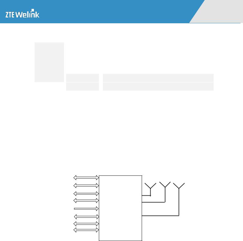
2.2Function Overview
2.2.1Baseband Function
When connect the module product ZM8620_V2 to the system board, there are several main signal groups as follows: USB signal, SIM card signal, UART signal, GPIO signal, SPI signal, power on and resetting signal, wakeup signal, power supply and ground. At the same time, ZM8620_V2 has the main antenna interface, diversity antenna interface, and GPS antenna interface.
USB |
GPS |
Main |
Diversity |
|
|
||||
Antenna |
Antenna |
|||
|
Antenna |
|||
|
|
|
||
SIM card |
|
|
|
|
UART |
|
|
|
|
GPIO |
ZM8620_V2 |
|
|
|
PCIE LTE wireless |
|
|
||
|
|
|
||
POWER |
Internet access |
|
|
|
module |
|
|
||
|
|
|
||
SPI |
|
|
|
|
GND |
|
|
|
|
WAKE#&PERST#&W |
|
|
|
|
_DISABLE Signals |
|
|
|
Figure 2–2 System Connection Diagram
2.2.2Radio Frequency Function
The radio frequency function of ZM8620_V2 can be viewed from the aspect of over-the-air wireless bearer network, frequency band, whether receive diversity feature is supported.
(a) Support LTE FDD, LTE TDD, UMTS;
All Rights reserved, No Spreading abroad without Permission of ZTEWelink |
7 |
 Loading...