


 Loading...
XM-444W
SERVICE MANUAL
US Model
Ver 1.1 2003. 02
SPECIFICATIONS
AUDIO POWER SPECIFICATIONS
POWER OUTPUT AND TOTAL HARMONIC DISTORTION
35 watts per channel minimum continuous average power into 4 ohms, both channels driven from 20 Hz to 20 kHz with no more than 0.04% total harmonic distortion per Car Audio Ad Hoc Committee standards.
Other Specifications
Circuit system |
OTL (output transformerless) circuit Pulse |
|
power supply |
Inputs |
RCA pin jacks |
|
High level input connector |
Input level adjustment range |
|
|
0.3 – 6 V (RCA pin jacks), |
|
0.6 – 12 V (High level input) |
Outputs |
Speaker terminals |
Speaker impedance |
2 – 8 Ω (stereo) |
|
4 – 8 Ω (when used as a bridging amplifier) |
Maximum outputs |
|
4 Speakers: |
80 W × 4 (at 4 Ω) |
3 Speakers: |
80 W × 2 + 222 W × 1 (at 4 Ω) |
2 Speakers: |
222 W × 2 (at 4 Ω) |
Rated outputs (supply voltage at 14.4 V) |
|
4 Speakers: |
35 W × 4 (20 Hz – 20 kHz, 0.04% THD, at 4 Ω) |
|
40 W × 4 (20 Hz – 20 kHz, 0.1% THD, at 2 Ω) |
2 Speakers: |
80 W × 2 (20 Hz – 20 kHz, 0.1% THD, at 4 Ω) |
Frequency response |
5 Hz – 80 kHz ( +0–3 dB) |
Harmonic distortion |
0.005% or less (at 1 kHz, 4 Ω, 10 W) |
Low-pass filter |
80 Hz, –18 dB/oct |
High-pass filter |
80 Hz, –12 dB/oct |
Power requirements |
12 V DC car battery |
|
(negative ground) |
Power supply voltage |
10.5 – 16 V |
Current drain |
at rated output : 20 A (4 Ω, 35 W × 4) |
|
Remote input : 1.5 mA |
Dimensions |
Approx. 260 × 55 × 180 mm (w/h/d) not incl. |
|
projecting parts and controls |
Mass |
Approx. 2.4 kg not incl. accessories |
Supplied accessories |
Mounting screws (4) |
|
High level input cord (1) |
|
Protection cap (1) |
Design and specifications are subject to c hange without
notice.
STEREO POWER AMPLIFIER
9-873-977-02 Sony Corporation
2003B0400-1 e Vehicle Company
© 2003. 02 |
Published by Sony Engineering Corporation |
1
XM-444W
PROTECTOR OPERATION CHECK
Thermal Protect
1.Short across TH801 with the power on.
2.Verify that the protector is operated and LD801 illuminates red.
3.Verify that the protector is released and LD801 illuminates green when the short is removed.
4.Likewise, perform items 1 to 3 for TH802 and TH803.
Over Current Protect
1.Short between the positive and negative sides of the speaker output terminal CN802 with the power on.
(Perform this shorting for each channel on FRONT and REAR.)
2.Verify that the protector is operated and LD801 illuminates red.
3.Verify that the protector is not released and LD801 remains red even when the short is removed.
4.Verify that the protector is released and LD801 illuminates green when the power is turned off and then on again.
Offset Protect
1.Short between the +12V terminal of CN801 and the BTL+ or BTL– of the speaker output terminal CN802.
(Short between +12V terminal and BTL+ and between +12V terminal and BTL–.)
2.Verify that the protector is operated and LD801 illuminates red.
3.Verify that the protector is not released and LD801 remains red even when the short is removed.
4.Verify that the protector is released and LD801 illuminates green when the power is turned off and then on again.
Chassis Short Protect
1.Short between the +12V terminal of CN801 and the chassis with the power on.
2.Verify that the pilot lamp PL801 goes on.
3.Verify that PL801 goes off when the short is removed.
TABLE OF CONTENTS
1. GENERAL
Connections ............................................................................. |
3 |
2. DISASSEMBLY
2-1. |
Bottom Plate ........................................................................ |
5 |
2-2. |
Heat Sink ............................................................................. |
6 |
2-3. |
Amp Board .......................................................................... |
6 |
3. DIAGRAMS
3-1. Block Diagram –Front Section– ......................................... |
7 |
|
3-2. |
Block Diagram –Rear/Power Section– ............................... |
8 |
3-3. |
Schematic Diagram –Amp Section– ................................... |
9 |
3-4. |
Schematic Diagram –Power Section– ............................... |
10 |
3-5. |
Printed Wiring Board ........................................................ |
11 |
4. EXPLODED VIEW ........................................................... |
12 |
|
5. ELECTRICAL PARTS LIST ......................................... |
13 |
|
Notes on Chip Component Replacement
•Never reuse a disconnected chip component.
•Notice that the minus side of a tantalum capacitor may be damaged by heat.
SAFETY-RELATED COMPONENT WARNING!!
COMPONENTS IDENTIFIED BY MARK 0 OR DOTTED LINE WITH MARK 0 ON THE SCHEMATIC DIAGRAMS AND IN
THE PARTS LIST ARE CRITICAL TO SAFE OPERATION. REPLACE THESE COMPONENTS WITH SONY PARTS WHOSE PART NUMBERS APPEAR AS SHOWN IN THIS MANUAL OR IN SUPPLEMENTS PUBLISHED BY SONY.
2

XM-444W
SECTION 1
GENERAL This section is extracted from instruction manual.
3

XM-444W
4

XM-444W
SECTION 2
DISASSEMBLY
Note : This set can be disassemble according to the following sequence.
SET
2-1. BOTTOM PLATE (Page 5)
2-2. HEAT SINK (Page 6)
2-3. AMP BOARD (Page 6)
Note : Follow the disassembly procedure in the numerical order given.
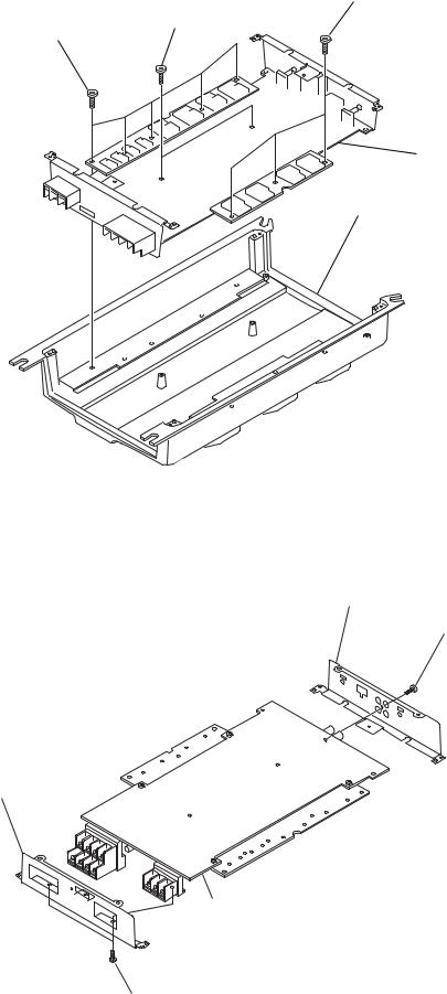
2-1. BOTTOM PLATE
1 BTP 3x6
3 bottom plate
2 BTP 3x6
5
XM-444W
2-2. HEAT SINK
1 BVTP 3x8
3 BVTP 3x8
2 BVTP 3x8
4 AMP board
5 heat sink
2-3. AMP BOARD
2 rear panel
1 BVTP 3x8
4 front panel
5 AMP board
3 BVTP 3x8
6
Loading...