


CM-H777RC/H888RC
AMPS
SERVICE MANUAL
For Technical Service
TABLE OF CONTENTS
1. SERVICING NOTES ............................................... |
2 |
2.CIRCUIT DESCRIPTION
2-1. |
Logic Circuit Description ................................................ |
3 |
2-2. |
Radio Circuit Description ................................................ |
4 |
2-3. |
Power Supply Flow Chart ................................................ |
5 |
3. |
TOOLS .......................................................................... |
6 |
4. |
TROUBLE SHOOTING .......................................... |
9 |
5.DIAGRAMS
5-1. |
Frame Schematic Diagram .............................................. |
18 |
5-2. |
Note for Printed Wiring Boards and |
|
|
Schematic diagrams ........................................................ |
22 |
5-3. |
Printed Wiring Board |
|
|
– RAGIC Board (RF/LOGIC Section) – ......................... |
23 |
5-4. |
Schematic Diagram |
|
|
– RAGIC Board (1/2) (RF Section) – .............................. |
25 |
5-5. |
Schematic Diagram |
|
|
– RAGIC Board (2/2) (LOGIC Section) – ...................... |
27 |
5-6. |
Printed Wiring Board |
|
|
– I/F Section – ................................................................. |
29 |
5-7. |
Schematic Diagram |
|
|
– I/F Section – ................................................................. |
31 |
6. |
ELECTRICAL PARTS LIST ................................ |
33 |

SECTION 1
SERVICING NOTES
• Model Identification
Serial No.
CM-H777RC: 148371 ~ 1560720
CM-H888RC: 1172577 ~ 1248576
• Combination of Boards
Combination of RAGIC board and Interface board for current CM-H777/H888 and CM-H777RC/H888RC
I/F board |
CM-H777/H888 I/F board |
CM-H777RC/H888RC I/F board |
|
RAGIC board |
|||
|
|
||
CM-H777/H888 RAGIC board |
— |
OK |
|
CM-H777RC/H888RC RAGIC board |
OK |
— |
Flexible Circuit Board Repairing
•Keep the temperature of the soldering iron around 270 ºC during repairing.
•Do not touch the soldering iron on the same conductor of the circuit board (within 3 times).
•Be careful not to apply force on the conductor when soldering or unsoldering.
Notes on chip component replacement
•Never reuse a disconnected chip component.
•Notice that minus side of a tantalum capacitor may be damaged by heat.
Note for the replacement of AT24C32N-10SI-2.7 (U8A)
• IC AT24C32N-10SI-2.7 (E2 PROM) of RAGIC mounted circuit board is not available itself due to the volume data characteristics for audio and etc. is difference each IC.
Therefore, the RAGIC board have to replace completely.
– 2 –
SECTION 2
CIRCUIT DESCRIPTION
2-1. LOGIC CIRCUIT DESCRIPTION
The functional block diagram is shown in LOGIC CIRCUIT BLOCK DIAGRAM.
The logic circuit consists of the following parts.
•MPU (including Digital processor)
•EEPROM, 32 kbits
•FEEPROM, 128 kbytes
•Audio signal processor
•Power supply IC
•LCD driver (Interface Board)
•20-digit dot matrix liquid crystal display (Interface Board)
The audio from the microphone is amplified at the microphone amplifier, goes through the analog switch and transmit audio is input at the transmit-audio terminal. The analog switch can be turned off with Command 5100 (Change-path) of the test set when the characteristics of transmit audio of the radio unit is measured.
The audio is compressed at the compressor. The compressor output does through the band pass filter, pre-emphasis, deviation limiter, and post-deviation filter, and is added with the control signal at the audio signal processor. The summed signal is applied to the modulation input terminal of the radio portion.
The demodulated signal from the receiver goes through the deemphasis circuit in the audio signal processor, the band pass filter and the expander, and is added at the summing amplifier with the tone signal. The summed signal is applied to the receive audio terminal.
Analog SW, Compressor and expander is in the Audio signal processor.
For wideband data transmission, the data signal is first encoded into the BCH code with the software for the MPU. The BCH code is sent via the 8-bit data bus to digital processor (KE5A220 or KE5A221). The parallel data bus is converted to serial data to the 32-bit shift register of digital signal is sent to the audio signal processor.
In the audio signal processor, the Manchester code signal goes through analog switch, variable resistor T.DATA VR5 (variable from +1.6 to –1.4 dB in 0.2 dB steps), the 4th order low pass filter with 20 kHz cut-off frequency and lastly TX VR3 (variable from –2.5 dB to –15.2 dB in 0.1 dB steps), and then appears at the FMMOD terminal.
Supervisory audio tones (SAT: 6030 Hz, 6000 Hz, 5970 Hz) are demodulated at the radio portion and appears at the FMDEM terminal. The SAT signal is then applied to the logic portion. The SAT signal goes through the band pass filter having the 6-kHz center frequency in the audio signal processor, and is converted to logic level signal through the comparator. The logic level signal is phase-synchronized at the digital phase locked loop in digital processor. The comparator output goes through SAT data remark and, the low pass filter, TSAT VR6 (variable from –9.6 to –14.1 dB in 0.3 dB steps), analog switch in the audio signal processor. Thereafter, the SAT signal takes the same signal processing route as the wide band data signal.
Dual Tone Multipul-Frequency signal is generated at the audio signal processor, and the signal is converted into sine wave. Then the sine wave signal is passed through DTMF VR10. After that, the signal takes the same signal processing route as voice.
Wide band data signal is applied to the audio signal processor via FMDEM terminal, and is converted into the logic level signal at the comparator. Then the signal goes to the digital processor (KE5A220 or KE5A221) and acquires bit synchronization at the digital phase locked loop circuit. Next, the signal is converted into non-return zero signal from Manchester code at the integrated and dump circuit. From this signal Barker code (11100010010) is detected at the word synchronizing detection circuit, and then the information and parity bit signal (40 bits) is cleaned up by a 3/5 majority vote circuit.
From the signal, syndrome is detected at the syndrome detector, and an interrupt is requested on the MPU to inform the reception of the signal. When an interrupt occurs the software of the MPU allows 28 information bits and 12 parity bits to enter the MPU by way of data bus. The software checks syndrome at first, then will do error correction, if there are any.
2-2. RADIO CIRCUIT DESCRIPTION
2-2-1. General Description
The functional block diagram is shown in the radio circuit block diagram.
Signals received from the cell site pass through the duplexer to the receiver circuit, where they are amplified and demodulated. The received signals may be voice and/or coded signaling information. From the receiver circuit, voice signals and coded signaling information are sent to the logic circuit.
To transmit signals, the Transmitter carrier is frequency-modula- tion with voice and/or coded signaling information. The carrier is then passed through a duplexer to the antenna.
2-2-2. Synthesizer Circuit
The equipment has two phase-locked-loop frequency synthesizer. One is used to produce the RF modulator. Another one is used to produce the RF signals for 1st local oscillator injections of the receiver.
The synthesizer of 1st local and TX local oscillator (U306) controls an RF signal, between 941 MHz and 966 MHz, or 824 MHz, and 849 MHz according to a DC control voltage. The internal dual modules prescaler divides the signal from the buffer amplifier by 128 or 129. The output of a portion of the programmable divider function determines whether 128 or 129 is a divider. Channel assignment numbers are determined by a 18 bit serial data input sequence from the logic circuit.
The phase detector compares the phases of the two signals from the dividers and drivers the charge pump according to the comparison result. If the loop goes out of lock, the phase detector generates an unlock detect signal.
The charge pump translates the digital output of the phase detector into a current source or sink (depending on the phase information). The low-pass filter integrates this change in correct to produce the DC voltage that controls the VCO (U305 and U404) output frequency.
The 14.4 MHz TCXO (U307) output is divided by 960 to produce the 15.0 kHz reference frequency for the synthesizer.
– 3 –
2-2-3. Transmitter Circuit
The modulator generates transmit signal with VCO and to fed the discrete switch circuit.
The output signal of the discrete switch circuit is fed to the power amplifier (U402).
The output signal of the power amplifier is fed to the directional coupler (U401) and then the duplexer filter (FL401).
A sample of the RF output power is coupled off, and passed through the detector (CR401) and fed to the logic circuit for APC loop.
The p-cont signal from the logic circuit controls power amplifier level controllers (Q403, Q405) to control the power amplifier (U402) output level.
2-2-4. Receiver Circuit
The receiver is a double conversion super-heterodyne receiver, capable of receiving frequencies from 869 MHz to 894 MHz.
The RX signal from duplexer filter (FL401) is amplified by LNA (Q301) with band-pass filter (FL301) and fed to the double balanced mixer (U301).
The synthesizer output signal is also fed to the mixer to obtain the first IF signal (72.06 MHz).
The first IF signal is fed to the second mixer through first amplifier (Q303) and x’tal filter (FL302) and then heterodyned with a fixed 72 MHz second local VCO signal obtain a 60 kHz second IF signal.
The second local oscillator signal is produce by signal synthesizer (U304) and discrete VCO.
After this frequency conversion, the signal second IF fed to the monolithic low-power IF system (U302) incorporating two limiting IF amplifiers quadrature detector, logarithmic signal strength indication (RSSI) and voltage regulator.
The detected output signal and RSSI signal are fed to the logic circuit.
– 4 –
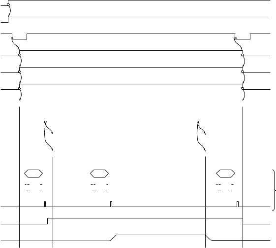
2-3. POWER SUPPLY FLOW CHART
+B |
|
|
|
BATTERY |
|
|
|
||
|
VDD B (U3 pin 3)
VDD U
ON |
OFF |
Power SW
R1 ON
(U3 pin $¢)
VDD
Rx En (U3 pin 7, !º)
VDD 1, VDD 2 |
|
|
|
|
|
|
|
|
|
|
|
|
|
|
|
|
|
|
|
|
|
|
|
|
|
|
|
|
|
|
|
|
|
|
|
|
|
|
|
|
|
|
|
|
|
SEND key |
|
|
|
|
|
|
|
|
|
|
|
|
|
|
SEND |
END |
|||||||||||||||||||||||||||||
|
|
|
|
|
|
|
|
|
|
|
|
|
|
|
|
|
|
|
|
|
|
|
|
|
|
|
|
|
|
|
|
|
|
|
|
|
|
|
|
|
|
|
|
|
|
End key |
|
|
|
|
|
|
|
|
|
|
|
|
|
|
|
|
|
|
|
|
|
|
|
|
|
|
|
|
|
|
|
|
|
|
|
|
|
|
|
|
|
|
|
|
|
|
|
|
|
|
|
|
|
|
|
|
|
|
|
|
|
|
|
|
|
|
|
|
|
|
|
|
|
|
|
|
|
|
|
|
|
|
|
|
|
|
|
|
|
|
|
Tx EN |
|
|
|
|
|
|
|
|
|
|
|
|
|
|
|
|
|
|
|
|
|
|
|
|
|
|
|
|
|
|
|
|
|
|
|
|
|
|
|
|
|
|
|
|
LogicnRF |
|
|
|
|
|
|
|
|
|
|
|
|
|
|
|
|
|
|
|
|
|
|
|
|
|
|
|
|
|
|
|
|
|
|
|
|
|
|
|
|
|
|
|
|
||
(U405 pin 1) |
|
|
|
|
|
|
|
|
|
|
|
|
|
|
|
|
|
|
|
|
|
|
|
|
|
|
|
|
|
|
|
|
|
|
|
|
|
|
|
|
|
|
|
|
|
|
|
|
|
|
|
|
|
|
|
|
|
|
|
|
|
|
|
|
|
|
|
|
|
|
|
|
|
|
|
|
|
|
|
|
|
|
|
|
|
|
|
|
|
LogicnRF |
|
VDD T |
|
|
|
|
|
|
|
|
|
|
|
|
|
|
|
|
|
|
|
|
|
|
|
|
|
|
|
|
|
|
|
|
|
|
|
|
|
|
|
|
|
|
|
|
|
|
|
|
|
|
|
|
|
|
|
|
|
|
|
|
|
|
|
|
|
|
|
|
|
|
|
|
|
|
|
|
|
|
|
|
|
|
|
|
|
|
|
|
|
||
SYNTHESIZER |
|
|
|
|
|
|
|
C ch |
|
|
|
|
|
|
|
|
V ch |
|
|
|
|
|
|
|
|
C ch |
|||||||||||||||||||
U306 pin !™ |
|
|
|
|
|
|
|
|
|
|
|
|
|
|
|
|
|
|
|
|
|
|
|
|
|
|
|
|
|
|
|
|
|
|
|
|
|
|
|
|
|
|
|
|
|
|
|
|
|
|
|
|
|
|
|
|
|
|
|
|
|
|
|
|
|
|
|
|
|
|
|
|
|
|
|
|
|
|
|
|
|
|
|
|
|
|
|
|
|
|
|
(SYN DATA) |
|
|
|
|
|
|
|
|
|
|
|
|
|
|
|
|
|
|
|
|
|
|
|
|
|
|
|
|
|
|
|
|
|
|
|
|
|
|
|
|
|
|
|
|
|
U306 pin !¡ |
|
|
|
|
|
|
|
|
...... |
|
|
|
|
|
|
|
|
|
|
|
|
...... |
|
|
|
|
|
|
|
|
|
|
|
|
...... |
|
|
|
|
LogicnRF |
|||||
|
|
|
|
|
|
|
|
|
|
|
|
|
|
|
|
|
|
|
|||||||||||||||||||||||||||
(SYN CLK) |
|
|
|
|
|
|
|
|
|
|
|
|
|
|
|
|
|
|
|
|
|
|
|
|
|
|
|
|
|
|
|
|
|
|
|
|
|
|
|
|
|
|
|
|
|
|
|
|
|
|
|
|
|
|
|
|
|
|
|
|
|
|
|
|
|
|
|
|
|
|
|
|
|
|
|
|
|
|
|
|
|
|
|
|
|
|
|
|
|
||
U306 pin !£ |
|
|
(SYN STB) |
|
|
LOCKDET 1 |
RFnLogic |
|
(U1A pin * ) |
||
|
||
RF Power |
LogicnRF |
|
(U402 pin !™) |
||
|
– 5 –

|
|
|
SECTION 3 |
|
|
|
|
|
TOOLS |
|
|
|
|
|
Fig. |
Description |
Part No. |
|
Remarks |
|
|
|
|
|
1 |
LR Screw Bit |
3-387-376-01 |
|
Special shape Bit |
|
For removing the screw of the rear cabinet Assy. |
|||
|
|
|
|
|
|
|
|
|
|
2 |
Converter Box |
3-702-720-01 |
|
RC232C Interface Box |
3 |
Test Cable G |
3-702-721-01 |
|
Test cable for Alignment. |
|
|
|
|
|
4 |
Selectable connector 1 |
3-702-735-01 |
|
Connector for monitoring software version |
|
|
|
|
|
5 |
Test Cable H |
3-702-726-01 |
|
Test cable for Auto NAM |
|
|
|
|
|
6 |
Connector 1 |
3-702-725-01 |
|
Connector for monitoring software version |
|
|
|
|
|
7 |
Floppy disk for User's |
3-702-724-01 |
|
|
|
information |
|
|
|
8 |
Floppy disk for Test |
3-702-727-01 |
|
Including Test Command for CM-H888 and |
|
command |
|
|
CM-H333 |
9 |
ANT driver |
3-702-580-01 |
|
|
|
|
|
|
|
1 LR Screw Bit |
5 Test Cable H |
|
Modular |
|
Jack |
|
6 Connector 1 |
2 Converter box (with AC Adaptor) |
|
|
7, 8 Floppy disk |
|
This floppy disk can be used commonly to CM-H777/H888 |
|
and others. |
3 Test Cable G |
RED (B+) |
|
|
||
To RF |
BLACK (GND) |
|
UDC |
9 pin |
|
D-sub |
||
Connector |
||
connector |
||
|
||
|
To Converter box |
9 ANT driver
YELLOW |
To TX-Audio |
|
To RX-Audio |
||
|
GREEN
4Selectable Connector 1
•You can check either a software version or the Lock code.
Resistor Item
1 kΩ Software ver. display
10 kΩ Lock code Over-ride
– 6 –

[Connecting CM-H777RC/H888RC and HP-8920A]
Use test cable G when measuring CM-H777RC/H888RC with HP-8920A.
|
|
|
Power Supply |
IBM-PC (not supplied) |
||
|
|
|
5.8 V DC |
|||
|
|
|
|
|
||
|
Cellular Tester |
|
|
|
|
|
|
HP-8920A |
|
|
|
|
|
|
|
|
RED |
BLACK |
|
|
|
|
|
(+B) |
(GND) |
9 pin |
|
|
|
|
|
|
|
|
|
|
|
|
|
D-Sub |
|
|
|
|
|
|
(not supplied) |
|
|
|
RF |
GREEN |
|
Tester Cable G |
|
|
|
|
|
|
||
|
|
YELLOW |
|
|
|
|
|
|
|
|
|
25 pin |
To AC outlet |
|
|
|
|
|
D-Sub |
(120 V) |
|
|
|
|
|
9 pin |
|
|
|
|
|
|
D-Sub |
|
|
|
|
|
|
Converter box |
|
|
|
|
|
|
To DC in |
|
• Volume position switch |
|
|
|
|
||
|
Position |
Remarks |
|
|
|
|
|
1 kΩ |
For software download |
|
|
|
|
Test |
10 kΩ |
Alignment, Auto NAM, |
|
|
|
|
User's information, Test command |
|
|
|
|||
Cable G |
|
|
|
|
||
68 kΩ |
Hand-free mode |
|
|
|
|
|
|
open |
Hand-set mode |
|
|
|
|
* Set to 10 kΩ |
|
|
|
|
|
|
[Connecting CM-H777RC/H888RC and test cable H for Auto NAM]
from PC 
To AC outlet
converter box 

To DC in
Test Cable H
– 7 –
[Connecting connector 1 to CM-H777RC/H888RC]
You can read the current software version by turning the power on after connecting the connector 1 or selectable connector 1 first.
Connector 1
Connect the connector 1 first, and then turn the power on.
LCD Display
Ready –210201–
[HP8920 test condition for alignment program]
1)RF Cable loss setting
1 Press key “SIFT” + “CONFIG”
2 Set RF Level offset “ON”
3 Set RF IN/OUT “–0.7” dB (Input RF cable loss)
2)Adjust TX power levels 1 Press key “TX TEST”
2 Setting Tune mode “Auto”
3)Adjust signal modulation
1 Press key “TX TEST”
2 Setting condition at HP8920A in accordance with the display of the computer
3 Setting Tune mode “Auto”
4 Setting AF Anl In “FM Demod”
5 Setting Detector “RMS*SQRT2”
6 Setting IF Filter “230 kHz”
7 Setting Filter 1 “300 Hz HP”
8 Setting Filter 2 “15 kHz LP”
9 Setting De-Emphasis “off”
4)Adjust demodulation
1 Press key “RX TEST”
2 Setting condition at HP8920A in accordance with the
display of the computer 3 Setting Load “600 Ω”
4 Setting Filter 1 “300 Hz HP”
5 Setting Filter 2 “C-MESSAGE”
5)Adjust RSSI thresholds 1 Press key “RX TEST”
2 Setting condition at HP8920A in accordance with the display of the computer
– 8 –
SECTION 4
TROUBLE SHOOTING
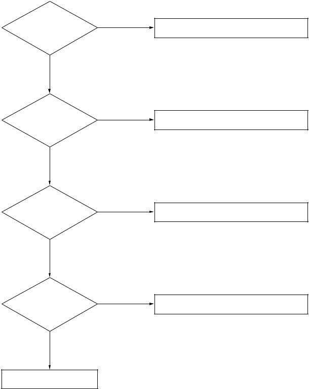
4-1. Cant’t power supply on
+B more than 4.5 V
YES
U1A (MPU) #34 0 V pushing PWR key
YES
VDD (U3 #1) |
3.3 V |
VDDB (U3 #3) |
3.3 V |
VDDU (U1A #37) |
3.3 V |
YES
U1A (MPU) #27
7.68 MHz above 2.8 VDD
YES
Check U2 and U8A
NO
NO
NO
NO
Check +B line area
Check PSSW line area
Check VDD, VDDB and VDDU line area
Check clock circuit area (U1A – Y1)
– 9 –
 Loading...