


SGS Thomson Microelectronics VN820SP13TR, VN820SP, VN820SO, VN820PT13TR, VN820PT Datasheet
...
|
|
VN820 / VN820SO |
® |
/ VN820SP |
/ VN820-B5 / VN820PT |
|
|
|
|
|
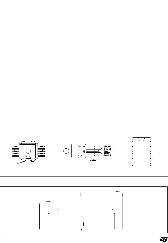
HIGH SIDE DRIVER |
|
|
|
TYPE |
RDS(on) |
IOUT |
VCC |
VN820 |
|
|
|
VN820SP |
|
|
|
VN820-B5 |
40 mΩ |
9 A |
36 V |
VN820SO |
|
|
|
VN820PT |
|
|
|
|
|
|
|
■CMOS COMPATIBLE INPUT
■ON STATE OPEN LOAD DETECTION
■OFF STATE OPEN LOAD DETECTION
■SHORTED LOAD PROTECTION
■UNDERVOLTAGE AND OVERVOLTAGE SHUTDOWN
■PROTECTION AGAINST LOSS OF GROUND
■VERY LOW STAND-BY CURRENT
■REVERSE BATTERY PROTECTION (*)
DESCRIPTION
The VN820, VN820SP, VN820-B5, VN820SO, VN820PT are monolithic devices made by using STMicroelectronics VIPower M0-3 Technology, intended for driving any kind of load with one side connected to ground.
Active VCC pin voltage clamp protects the device against low energy spikes (see ISO7637 transient
BLOCK DIAGRAM
10 |
|
|
1 |
|
|
PowerSO-10™ |
P2PAK |
PPAK |
|
|
|
|
|
|
|
PENTAWATT |
SO-16L |
|||||
|
|
|
||||
|
|
ORDER CODES |
||||
PACKAGE |
|
|
TUBE |
|
T&R |
|
|
|
|
|
|
|
|
PENTAWATT |
|
|
VN820 |
|
- |
|
|
|
|
|
|||
PowerSO-10™ |
VN820SP |
|
VN820SP13TR |
|||
P2PAK |
|
|
VN820-B5 |
|
VN820-B513TR |
|
SO-16L |
|
|
VN820SO |
|
VN820SO13TR |
|
PPAK |
|
|
VN820PT |
|
VN820PT13TR |
|
|
|
|
|
|
|
|
compatibility table). Active current limitation combined with thermal shutdown and automatic restart protect the device against overload.
The device detects open load condition both is on and off state. Output shorted to VCC is detected in
the off state. Device automatically turns off in case of ground pin disconnection.
VCC
VCC |
|
OVERVOLTAGE |
CLAMP |
|
DETECTION |
|
|
UNDERVOLTAGE |
|
|
DETECTION |
GND |
|
|
|
|
Power CLAMP |
INPUT |
|
DRIVER |
|
OUTPUT |
|
|
LOGIC |
|
|
|
|
|
|
CURRENT LIMITER |
STATUS |
|
ON STATE OPENLOAD |
|
|
DETECTION |
OVERTEMPERATURE |
|
OFF STATE OPENLOAD |
DETECTION |
|
|
|
|
AND OUTPUT SHORTED TO VCC |
|
|
DETECTION |
(*) See application schematic at page 9
June 2003 |
1/34 |
VN820 / VN820SO / VN820SP / VN820-B5 / VN820PT
ABSOLUTE MAXIMUM RATING
Symbol |
Parameter |
|
|
Value |
|
|
|
Unit |
|
|
|
|
|
|
|
||||
|
PowerSO-10™ |
PENTAWATT |
P2PAK |
SO-16L |
PPAK |
||||
VCC |
DC Supply Voltage |
|
41 |
|
|
|
|
V |
|
- VCC |
Reverse DC Supply Voltage |
|
- 0.3 |
|
|
|
|
V |
|
- IGND |
DC Reverse Ground Pin Current |
|
- 200 |
|
|
|
|
mA |
|
IOUT |
DC Output Current |
|
Internally Limited |
|
|
A |
|||
- IOUT |
Reverse DC Output Current |
|
- 9 |
|
|
|
|
A |
|
IIN |
DC Input Current |
|
+/- 10 |
|
|
|
|
mA |
|
ISTAT |
DC Status Current |
|
+/- 10 |
|
|
|
|
mA |
|
|
Electrostatic Discharge |
|
|
|
|
|
|
|
|
|
(Human Body Model: R=1.5KΩ; C=100pF) |
|
|
|
|
|
|
|
|
VESD |
- INPUT |
|
4000 |
|
|
|
|
V |
|
- STATUS |
|
4000 |
|
|
|
|
V |
||
|
|
|
|
|
|
||||
|
- OUTPUT |
|
5000 |
|
|
|
|
V |
|
|
- VCC |
|
5000 |
|
|
|
|
V |
|
EMAX |
Maximum Switching Energy (L=4mH; RL=0Ω; |
481 |
|
|
481 |
|
|
mJ |
|
Vbat=13.5V; Tjstart=150ºC; IL=13A) |
|
|
|
|
|||||
|
|
|
|
|
|
|
|
||
EMAX |
Maximum Switching Energy (L=3.7mH; |
|
|
|
|
438 |
|
mJ |
|
RL=0Ω; Vbat=13.5V; Tjstart=150ºC; IL=13A) |
|
|
|
|
|
||||
|
|
|
|
|
|
|
|
||
EMAX |
Maximum Switching Energy (L=4.48mH; |
|
|
|
|
|
526 |
mJ |
|
RL=0Ω; Vbat=13.5V; Tjstart=150ºC; IL=13A) |
|
|
|
|
|
||||
|
|
|
|
|
|
|
|
||
Ptot |
Power Dissipation TC=25°C |
65.8 |
65.8 |
|
65.8 |
8.3 |
65.8 |
W |
|
Tj |
Junction Operating Temperature |
|
Internally Limited |
|
|
°C |
|||
Tc |
Case Operating Temperature |
|
- 40 to 150 |
|
|
|
°C |
||
Tstg |
Storage Temperature |
|
- 55 to 150 |
|
|
|
°C |
||
CONNECTION DIAGRAM (TOP VIEW)
GROUND |
6 |
5 |
INPUT |
7 |
4 |
STATUS |
8 |
3 |
N.C. |
9 |
2 |
N.C. |
10 |
1 |
|
|
|
|
|
11 |
|
VCC |
|
|
PowerSO-10™ |
|
|
VCC |
1 |
16 |
VCC |
|
N.C. |
|
|
OUTPUT |
OUTPUT |
GND |
|
|
OUTPUT |
OUTPUT |
|
|
||
INPUT |
|
|
OUTPUT |
|
N.C. |
|
|
||
OUTPUT |
STATUS |
|
|
OUTPUT |
OUTPUT |
|
|
||
N.C. |
|
|
OUTPUT |
|
|
|
|
||
PPAK / P2PAK / PENTAWATT |
N.C. |
|
|
OUTPUT |
VCC |
8 |
9 |
VCC |
SO-16L
CURRENT AND VOLTAGE CONVENTIONS
IS
|
IIN |
|
|
|
|
|
|
|
|
|
|
|
|
|
|
|
|
|
VCC |
|
|
|
|||||||||
|
|
|
|
INPUT |
|
|
|
|
|
|
|
|
|
|
|
|
|
|
|
|
|
|
|
|
|
|
|
|
|
|
|
|
|
ISTAT |
|
|
|
|
|
|
|
|
|
|
IOUT |
||
|
|
|
|
|
|
|
|
|
|
|
|
|
|||
|
|
|
|
STATUS |
|
|
|
|
|
|
OUTPUT |
|
|
|
VCC |
|
|
|
|
|
GND |
|
|
|
|||||||
|
|
|
|
|
|
|
|
|
|
|
|
|
|
|
|
|
VIN |
|
|
|
|
|
|
|
|
|
VOUT |
||||
|
VSTAT |
|
|
|
|
|
|
IGND |
|
||||||
|
|
|
|
|
|
|
|
|
|
|
|
|
|
|
|
2/34

VN820 / VN820SO / VN820SP / VN820-B5 / VN820PT
THERMAL DATA
Symbol |
Parameter |
|
|
|
Value |
|
|
|
Unit |
|
|
|
|
|
|
|
|||
|
|
PowerSO-10™ |
PENTAWATT |
P2PAK |
SO-16L |
PPAK |
|||
Rthj-case |
Thermal Resistance Junction-case |
Max |
1.9 |
1.9 |
1.9 |
- |
1.9 |
°C/W |
|
Rthj-lead |
Thermal Resistance Junction-lead |
Max |
- |
- |
- |
15 |
- |
°C/W |
|
Rthj-amb |
Thermal Resistance Junction-ambient Max |
51.9 (*) |
61.9 (*) |
51.9 (*) |
65 (**) |
76.9 (*) |
°C/W |
||
(*) When mounted on a standard single-sided FR-4 board with 0.5cm2 of Cu (at least 35μm thick). |
|
|
|
|
|
|
||||
(**) When mounted on FR4 printed circuit board with 0.5cm2 of Cu (at least 35μ thick) connected to all V |
CC |
pins. |
|
|
||||||
|
|
|
|
|
|
|
|
|
||
ELECTRICAL CHARACTERISTICS (8V<VCC<36V; -40°C <Tj<150°C unless otherwise specified) |
|
|||||||||
POWER |
|
|
|
|
|
|
|
|
|
|
|
|
|
|
|
|
|
|
|
|
|
Symbol |
Parameter |
Test Conditions |
|
Min |
|
|
Typ |
Max |
Unit |
|
|
|
|
|
|
|
|
|
|
|
|
VCC |
Operating Supply Voltage |
|
|
|
5.5 |
|
|
13 |
36 |
V |
VUSD |
Undervoltage Shut-down |
|
|
|
3 |
|
|
4 |
5.5 |
V |
VUSDhyst |
Undervoltage Shut-down |
|
|
|
|
|
|
0.5 |
|
V |
hysteresis |
|
|
|
|
|
|
|
|||
VOV |
Overvoltage Shut-down |
|
|
|
36 |
|
|
|
|
V |
RON |
On State Resistance |
IOUT=3A; Tj=25°C; V CC>8V |
|
|
|
|
|
40 |
mΩ |
|
IOUT=3A; VCC>8V |
|
|
|
|
|
80 |
mΩ |
|||
|
|
|
|
|
|
|
||||
|
|
Off State; VCC=13V; VIN=VOUT=0V |
|
|
|
|
10 |
25 |
μA |
|
IS |
Supply Current |
Off State; VCC=13V; VIN=VOUT=0V; |
|
|
|
|
|
|
|
|
Tj=25°C |
|
|
|
|
10 |
20 |
μA |
|||
|
|
|
|
|
|
|||||
|
|
On State; VCC=13V; VIN=5V; IOUT=0A |
|
|
|
|
2 |
3.5 |
mA |
|
IL(off1) |
Off State Output Current |
VIN=VOUT=0V |
|
0 |
|
|
|
50 |
μA |
|
IL(off2) |
Off State Output Current |
VIN=0V; VOUT=3.5V |
|
-75 |
|
|
|
0 |
μA |
|
IL(off3) |
Off State Output Current |
VIN=VOUT=0V; Vcc=13V; Tj =125°C |
|
|
|
|
|
5 |
μA |
|
IL(off4) |
Off State Output Current |
VIN=VOUT=0V; Vcc=13V; Tj =25°C |
|
|
|
|
|
3 |
μA |
|
SWITCHING (VCC=13V) |
|
|
|
|
|
|
|
|
|
|
|
|
|
|
|
|
|
|
|
|
|
Symbol |
Parameter |
Test Conditions |
|
|
Min |
|
|
Typ |
Max |
Unit |
|
|
|
|
|
|
|
|
|
|
|
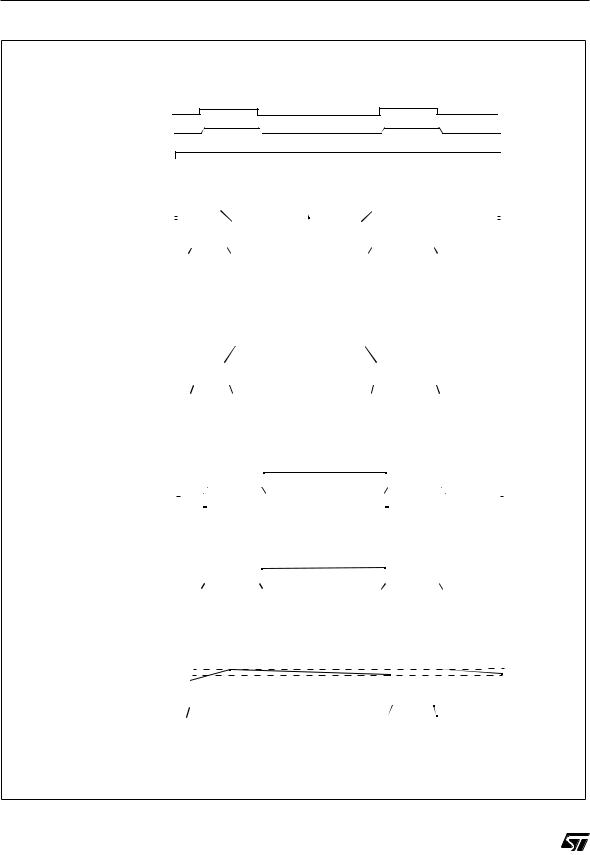
td(on) |
Turn-on Delay Time |
RL=4.3Ω from VIN rising edge to |
|
|
|
|
|
30 |
|
μs |
VOUT=1.3V |
|
|
|
|
|
|
||||
|
|
|
|
|
|
|
|
|
||
td(off) |
Turn-off Delay Time |
RL=4.3Ω from VIN falling edge to |
|
|
|
|
|
30 |
|
μs |
VOUT=11.7V |
|
|
|
|
|
|
||||
|
|
|
|
|
|
|
|
|
||
|
|
RL=4.3Ω from VOUT=1.3 to |
|
|
|
|
|
See |
|
|
dVOUT/dt(on) |
Turn-on Voltage Slope |
|
|
|
|
relative |
|
V/μs |
||
VOUT=10.4V |
|
|
|
|
|
|
||||
|
|
|
|
|
|
diagram |
|
|
||
|
|
|
|
|
|
|
|
|
|
|
|
|
RL=4.3Ω from VOUT=11.7 to |
|
|
|
|
|
See |
|
V/μs |
dVOUT/dt(off) |
Turn-off Voltage Slope |
|
|
|
|
relative |
|
|||
VOUT=1.3V |
|
|
|
|
|
|
||||
|
|
|
|
|
|
diagram |
|
|
||
|
|
|
|
|
|
|
|
|
|
|
INPUT PIN |
|
|
|
|
|
|
|
|
|
|
|
|
|
|
|
|
|
|
|
||
Symbol |
Parameter |
Test Conditions |
|
Min |
|
|
Typ |
Max |
Unit |
|
|
|
|
|
|
|
|
|
|
|
|
VIL |
Input Low Level |
|
|
|
|
|
|
|
1.25 |
V |
IIL |
Low Level Input Current |
VIN=1.25V |
|
1 |
|
|
|
|
μA |
|
VIH |
Input High Level |
|
|
|
3.25 |
|
|
|
|
V |
IIH |
High Level Input Current |
VIN=3.25V |
|
|
|
|
|
10 |
μA |
|
VI(hyst) |
Input Hysteresis Voltage |
|
|
|
0.5 |
|
|
|
|
V |
VICL |
Input Clamp Voltage |
IIN=1mA |
|
6 |
|
|
6.8 |
8 |
V |
|
IIN=-1mA |
|
|
|
|
-0.7 |
|
V |
|||
|
|
|
|
|
|
|
||||
|
|
|
|
|
|
|
|
|
|
3/34 |
|
|
|
|
|
|
|
|
|
|
|

VN820 / VN820SO / VN820SP / VN820-B5 / VN820PT
ELECTRICAL CHARACTERISTICS (continued)
STATUS PIN
Symbol |
Parameter |
Test Conditions |
Min |
Typ |
Max |
Unit |
|
|
|
|
|
|
|
VSTAT |
Status Low Output Voltage |
ISTAT=1.6mA |
|
|
0.5 |
V |
ILSTAT |
Status Leakage Current |
Normal Operation VSTAT=5V |
|
|
10 |
μA |
CSTAT |
Status Pin Input |
Normal Operation VSTAT=5V |
|
|
100 |
pF |
Capacitance |
|
|
||||
VSCL |
Status Clamp Voltage |
ISTAT=1mA |
6 |
6.8 |
8 |
V |
ISTAT=-1mA |
|
-0.7 |
|
V |
||
|
|
|
|
PROTECTIONS
Symbol |
Parameter |
Test Conditions |
Min |
Typ |
Max |
Unit |
|
|
|
|
|
|
|
|
|
TTSD |
Shut-down Temperature |
|
150 |
175 |
200 |
°C |
|
TR |
Reset Temperature |
|
135 |
|
|
°C |
|
Thyst |
Thermal Hysteresis |
|
7 |
15 |
|
°C |
|
tSDL |
Status delay in overload |
Tj>TTSD |
|
|
20 |
μs |
|
condition |
|
|
|||||
Ilim |
Current limitation |
|
9 |
13 |
20 |
A |
|
5.5V<VCC<36V |
|
|
20 |
A |
|||
|
|
|
|
||||
Vdemag |
Turn-off Output Clamp |
IOUT=3A; VIN=0V; L=6mH |
VCC-41 |
VCC-48 |
VCC-55 |
V |
|
Voltage |
|||||||
|
|
|
|
|
|
||
|
|
|
|
|
|
|
OPENLOAD DETECTION
Symbol |
Parameter |
Test Conditions |
Min |
Typ |
Max |
Unit |
|
IOL |
Openload ON State |
VIN=5V |
70 |
150 |
300 |
mA |
|
Detection Threshold |
|||||||
|
|
|
|
|
|
||
|
|
|
|
|
|
|
|
tDOL(on) |
Openload ON State |
IOUT=0A |
|
|
200 |
μs |
|
Detection Delay |
|
|
|||||
|
|
|
|
|
|
||
|
|
|
|
|
|
|
|
|
Openload OFF State |
|
|
|
|
|
|
VOL |
Voltage Detection |
VIN=0V |
1.5 |
2.5 |
3.5 |
V |
|
|
Threshold |
|
|
|
|
|
|
|
|
|
|
|
|
|
|
tDOL(off) |
Openload Detection Delay |
|
|
|
1000 |
μs |
|
at Turn Off |
|
|
|
OPEN LOAD STATUS TIMING (with external pull-up) |
|
|
|
|
OVERTEMP STATUS TIMING |
|||||||||||||||||
|
|
|
|
|
V |
OUT |
> V |
OL |
IOUT< IOL |
|
|
|
|
|
|
|
|
|
|
|
|
|
|
|
|
|
|
|
|
|
|
|
|
|
|
|
|
|
|
|
|
|
|
||
VIN |
|
|
|
|
|
|
|
|
|
|
|
|
|
|
|
Tj > TTSD |
|
|
|
|
|
|
|
|
|
|
|
|
|
|
|
|
|
|
|
|
|
|
|
||||||
|
|
|
|
|
|
|
|
|
|
|
|
|
|
|
|
|
||||||
|
|
|
|
|
|
|
|
|
|
VIN |
|
|
|
|
|
|
|
|
|
|||
|
|
|
|
|
|
|
|
|
|
|
|
|
|
|
|
|
|
|
|
|
|
|
|
|
|
|
|
|
|
|
|
|
|
|
|
|
|
|
|
|
|
|
|
|
|
|
|
|
|
|
|
|
|
|
|
|
|
|
|
|
|
|
|
|
|
|
|
|
|
|
|
|
|
|
|
|
|
|
|
|
|
|
|
|
|
|
|
|
|
|
|
VSTAT
VSTAT
tDOL(off) |
t |
DOL(on) |
|
t |
|
t |
SDL |
|
|
||||||
|
|
|
SDL |
|
|
4/34

|
|
VN820 / VN820SO / VN820SP / VN820-B5 / VN820PT |
Switching time Waveforms |
|
|
VOUT |
|
|
|
|
90% |
|
80% |
|
|
dVOUT/dt(on) |
dVOUT/dt(off) |
|
|
10% |
|
|
t |
VIN |
td(on) |
t |
|
|
d(off) |
t
TRUTH TABLE
CONDITIONS |
INPUT |
OUTPUT |
STATUS |
|
Normal Operation |
L |
L |
H |
|
H |
H |
H |
||
|
||||
|
|
|
|
|
|
L |
L |
H |
|
Current Limitation |
H |
X |
(Tj < TTSD) H |
|
|
H |
X |
(Tj > TTSD) L |
|
Overtemperature |
L |
L |
H |
|
H |
L |
L |
||
|
||||
|
|
|
|
|
Undervoltage |
L |
L |
X |
|
H |
L |
X |
||
|
||||
|
|
|
|
|
Overvoltage |
L |
L |
H |
|
H |
L |
H |
||
|
||||
|
|
|
|
|
Output Voltage > VOL |
L |
H |
L |
|
H |
H |
H |
||
|
|
|
|
|
Output Current < IOL |
L |
L |
H |
|
H |
H |
L |
||
|
|
|
|
5/34

VN820 / VN820SO / VN820SP / VN820-B5 / VN820PT
OPEN LOAD DETECTION IN OFF STATE
Off state open load detection requires an external pull-up resistor (RPU) connected between OUTPUT pin and a positive supply voltage (VPU) like the +5V line used to supply the microprocessor.
The external resistor has to be selected according to the following requirements:
1)no false open load indication when load is connected: in this case we have to avoid VOUT to be higher than
VOlmin; this results in the following condition VOUT=(VPU/(RL+RPU))RL<VOlmin.
2) no misdetection when load is disconnected: in this case the VOUT has to be higher than VOLmax; this results in the following condition RPU<(VPU–VOLmax)/
IL(off2).
Because Is(OFF) may significantly increase if Vout is pulled high (up to several mA), the pull-up resistor RPU should be connected to a supply that is switched OFF when the module is in standby.
The values of VOLmin, VOLmax and IL(off2) are available in the Electrical Characteristics section.
Open Load detection in off state
|
V batt. |
VPU |
|
VCC |
|
|
|
RPU |
INPUT |
DRIVER |
IL(off2) |
+ |
||
|
LOGIC |
|
|
|
OUT |
|
+ |
|
|
R |
|
STATUS |
- |
|
|
|
|
|
V |
|
|
OL |
R |
|
|
L |
|
GROUND |
|
6/34

VN820 / VN820SO / VN820SP / VN820-B5 / VN820PT
ELECTRICAL TRANSIENT REQUIREMENTS ON VCC PIN
ISO T/R 7637/1 |
|
|
TEST LEVELS |
|
|
|
Test Pulse |
|
I |
II |
III |
IV |
Delays and |
|
|
|
|
|
|
Impedance |
1 |
|
-25 V |
-50 V |
-75 V |
-100 V |
2 ms 10 Ω |
2 |
|
+25 V |
+50 V |
+75 V |
+100 V |
0.2 ms 10 Ω |
3a |
-25 V |
-50 V |
-100 V |
-150 V |
0.1 μs 50 Ω |
|
3b |
+25 V |
+50 V |
+75 V |
+100 V |
0.1 μs 50 Ω |
|
4 |
|
-4 V |
-5 V |
-6 V |
-7 V |
100 ms, 0.01 Ω |
5 |
|
+26.5 V |
+46.5 V |
+66.5 V |
+86.5 V |
400 ms, 2 Ω |
ISO T/R 7637/1 |
|
TEST LEVELS RESULTS |
|
||
Test Pulse |
|
I |
II |
III |
IV |
1 |
|
C |
C |
C |
C |
2 |
|
C |
C |
C |
C |
3a |
C |
C |
C |
C |
|
3b |
C |
C |
C |
C |
|
4 |
|
C |
C |
C |
C |
5 |
|
C |
E |
E |
E |
CLASS |
CONTENTS |
C |
All functions of the device are performed as designed after exposure to disturbance. |
EOne or more functions of the device is not performed as designed after exposure to disturbance and cannot be returned to proper operation without replacing the device.
7/34
VN820 / VN820SO / VN820SP / VN820-B5 / VN820PT
Figure 1: Waveforms
NORMAL OPERATION
INPUT
LOAD VOLTAGE
STATUS
|
|
|
|
|
|
|
|
|
|
|
|
|
|
|
|
|
|
|
UNDERVOLTAGE |
|
|
|
|
|
|
|
|
|
|
|
|
|
|
|
|
|
|
|
|
|
|
|
|
|
|
|
|
|
|
|
|
|
|
|
|
|
|
|
|
||||||||||||||||||||||||||||||||
VCC |
|
|
|
|
|
|
|
|
|
|
|
|
|
|
|
|
|
|
|
|
|
|
|
|
|
|
VUSDhyst |
|
|
|
|
|
|
|
|
|
|
|
|
|
|
|
|
|
|
|
|
|
|
|
|
|
|
|
|
|
|
|
|
|
|
|
|
|
|
|
|
||||||||||||||||||||||||
|
|
|
|
|
|
|
|
|
|
|
|
|
|
|
|
|
|
|
|
|
|
|
|
|
|
|
|
|
|
|
|
|
|
|
|
|
|
|
|
|
|
|
|
|
|
|
|
|
|
|
|
|
|
|
|
|
|
|
|
|
|
|
|
|
|
||||||||||||||||||||||||||
|
|
|
|
|
|
|
|
|
|
|
|
|
|
|
|
|
|
|
|
|
|
|
|
|
|
|
|
|
|
|
|
|
|
|
|
|
|
|
|
|
|
|
|
|
|
|
|
|
|
|
|
|
|
|
|
|
|
|
|
|
|
|
|
|
|
|
|
|
|
|
|
|
|
|
|
|
|
|
|
|
|
|
|
|
|
|
|
|
|
|
|
INPUT |
|
|
|
|
|
|
|
|
V |
USD |
|
|
|
|
|
|
|
|
|
|
|
|
|
|
|
|
|
|
|
|
|
|
|
|
|
|
|
|
|
|
|
|
|
|
|
|
|
|
|
|
|
|
|
|
|
|
|
|
|
|
|
|
|
|
|
|
|
|
|
|
|
|
|
|
|
|
|
|
|
|
|
|
|
||||||||
|
|
|
|
|
|
|
|
|
|
|
|
|
|
|
|
|
|
|
|
|
|
|
|
|
|
|
|
|
|
|
|
|
|
|
|
|
|
|
|
|
|
|
|
|
|
|
|
|
|
|
|
|
|
|
|
|
|
|
|
|
|
|
|
|
|
|
|
|
|
|
|
|
|
|
|
|
|
|
|
|
|
|
|
|
|
|
|
|
|
|
|
|
|
|
|
|
|
|
|
|
|
|
|
|
|
|
|
|
|
|
|
|
|
|
|
|
|
|
|
|
|
|
|
|
|
|
|
|
|
|
|
|
|
|
|
|
|
|
|
|
|
|
|
|
|
|
|
|
|
|
|
|
|
|
|
|
|
|
|
|
|
|
|
|
|
|
|
|
|
|
|
|
|
|
|
|
|
|
|
|
|
|
|
LOAD VOLTAGE |
|
|
|
|
|
|
|
|
|
|
|
|
|
|
|
|
|
|
|
|
|
|
|
|
|
|
|
|
|
|
|
|
|
|
|
|
|
|
|
|
|
|
|
|
|
|
|
|
|
|
|
|
|
|
|
|
|
|
|
|
|
|
|
|
|
|
|
|
|
|
|
|
|
|
|
|
|
|
|
|
|
|
|
|
|
|
|
|
|
|
|
|
|
|
|
|
|
|
|
|
|
|
|
|
|
|
|
|
|
|
|
|
|
|
|
|
|
|
|
|
|
|
|
|
|
|
|
|
|
|
|
|
|
|
|
|
|
|
|
|
|
|
|
|
|
|
|
|
|
|
|
|
|
|
|
|
|
|
|
|
|
|
|
|
|
|
|
|
|
|
|
|
|
|
|
|
|
|
|
|
|
|
|
|
|
|
|
|
|
|
|
|
|
|
|
|
|
|
|
|
|
|
|
|
|
|
|
|
|
|
|
|
|
|
|
|
|
|
|
|
|
|
|
|
|
|
|
|
|
|
|
|
|
|
|
|
|
|
|
|
|
|
|
|
|
|
|
|
|
|
|
|
|
|
|
|
|
|
|
|
|
|
|
|
|
|
|
|
|
|
|
|
|
|
|
STATUS |
|
|
|
|
|
|
|
|
|
|
|
|
|
|
|
|
|
|
|
|
|
|
|
|
|
|
|
|
|
|
|
|
|
|
|
|
|
|
|
|
|
|
|
|
|
|
|
|
|
|
|
|
|
|
|
|
|
|
|
|
|
|
|
|
|
|
|
|
|
|
|
|
|
|
|
|
|
|
|
|
|
|
|
|
|
|
|
|
|
|
|
|
|
|
|
|
|
|
|
|
|
|
|
|
|
|
|
|
|
|
|
|
undefined |
|
|
|
|
|
|
|
|
|
|
|
|
|
|
|
|
|
|
|
|
|
|
|
|
|
|
|
|
|
|
|
|
|
|
|
|
|
|
|
|
||||||||||||||||||||||||||||||
|
|
|
|
|
|
|
|
|
|
|
|
|
|
|
|
|
|
|
OVERVOLTAGE |
|
|
|
|
|
|
|
|
|
|
|
|
|
|
|
|
|
|
|
|
|
|
|
|
|
|
|
|
|
|
|
|
|
|
|
|
|
|
|
|
||||||||||||||||||||||||||||||||
|
|
|
|
VCC<VOV |
|
|
|
|
|
VCC>VOV |
|
|
|
|
|
|
|
|
|
|
|
|
|
|
|
|
|
|
|
|
|
|
|
|
|
|
|
|
|
|
|
|
|
|
|
|
|
|
|
|
|||||||||||||||||||||||||||||||||||||||||
VCC |
|
|
|
|
|
|
|
|
|
|
|
|
|
|
|
|
|
|
|
|
|
|
|
|
|
|
|
|
|
|
|
|
|
|
|
|
|
|
|
|
|
|
|
|
|
|
|
|
|
|
|
|
|
|
|
|
|
|
|
|
|
|
|
|
|
|
|
|
|
|
|
|
|
|
|
|
|
|
|
|
|
|
|
|
|
|
|
|
|
|
|
INPUT |
|
|
|
|
|
|
|
|
|
|
|
|
|
|
|
|
|
|
|
|
|
|
|
|
|
|
|
|
|
|
|
|
|
|
|
|
|
|
|
|
|
|
|
|
|
|
|
|
|
|
|
|
|
|
|
|
|
|
|
|
|
|
|
|
|
|
|
|
|
|
|
|
|
|
|
|
|
|
|
|
|
|
|
|
|
|
|
|
|
|
|
|
|
|
|
|
|
|
|
|
|
|
|
|
|
|
|
|
|
|
|
|
|
|
|
|
|
|
|
|
|
|
|
|
|
|
|
|
|
|
|
|
|
|
|
|
|
|
|
|
|
|
|
|
|
|
|
|
|
|
|
|
|
|
|
|
|
|
|
|
|
|
|
|
|
|
|
|
|
|
|
|
|
|
|
|
|
|
|
|
|
|
|
|
|
|
|
|
|
|
|
|
|
|
|
|
|
|
|
|
|
|
|
|
|
|
|
|
|
|
|
|
|
|
|
|
|
|
|
|
|
|
|
|
|
|
|
|
|
|
|
|
|
|
|
|
|
|
|
|
|
|
|
|
|
|
|
|
|
|
|
|
|
|
|
|
|
|
|
|
|
|
|
|
|
|
|
|
|
|
|
|
|
|
|
LOAD VOLTAGE |
|
|
|
|
|
|
|
|
|
|
|
|
|
|
|
|
|
|
|
|
|
|
|
|
|
|
|
|
|
|
|
|
|
|
|
|
|
|
|
|
|
|
|
|
|
|
|
|
|
|
|
|
|
|
|
|
|
|
|
|
|
|
|
|
|
|
|
|
|
|
|
|
|
|
|
|
|
|
|
|
|
|
|
|
|
|
|
|
|
|
|
|
|
|
|
|
|
|
|
|
|
|
|
|
|
|
|
|
|
|
|
|
|
|
|
|
|
|
|
|
|
|
|
|
|
|
|
|
|
|
|
|
|
|
|
|
|
|
|
|
|
|
|
|
|
|
|
|
|
|
|
|
|
|
|
|
|
|
|
|
|
|
|
|
|
|
|
|
|
|
|
|
|
|
|
|
|
|
|
|
|
|
|
|
|
|
|
|
|
|
|
|
|
|
|
|
|
|
|
|
|
|
|
|
|
|
|
|
|
|
|
|
|
|
|
|
|
|
|
|
|
|
|
|
|
|
|
|
|
|
|
|
|
|
|
|
|
|
|
|
|
|
|
|
|
|
|
|
|
|
|
|
|
|
|
|
|
|
|
|
|
|
|
|
|
|
|
|
|
|
|
|
|
|
|
STATUS |
|
|
|
|
|
|
|
|
|
|
|
|
|
|
|
|
|
|
|
|
|
|
|
|
|
|
|
|
|
|
|
|
|
|
|
|
|
|
|
|
|
|
|
|
|
|
|
|
|
|
|
|
|
|
|
|
|
|
|
|
|
|
|
|
|
|
|
|
|
|
|
|
|
|
|
|
|
|
|
|
|
|
|
|
|
|
|
|
|
|
|
|
|
|
|
|
|
|
OPEN LOAD with external pull-up |
|
|
|
|
|
|
|
|
|
|
|
|
|
|
|
|
|
|
|
|
|
|
|
|
|
|
|
|
|
|
|
|
|
|
|
|
|
|
|
|
||||||||||||||||||||||||||||||||||||||||||||
|
|
|
|
|
|
|
|
|
|
|
|
|
|
|
|
|
|
|
|
|
|
|
|
|
|
|
|
|
|
|
|
|
|
|
|
|
|
|
|
|
|
|
|
|
|
|
|
||||||||||||||||||||||||||||||||||||||||||||
INPUT |
|
|
|
|
|
|
|
|
|
|
|
|
|
|
|
|
|
|
|
|
|
|
|
|
|
|
VOUT>VOL |
|
|
|
|
|
|
|
|
|
|
|
|
|
|
|
|
|
|
|
|
|
|
|
|
|
|
|
|
|
|
|
|
|
|
|
|
|
|
|
|
||||||||||||||||||||||||
|
|
|
|
|
|
|
|
|
|
|
|
|
|
|
|
|
|
|
|
|
|
|
|
|
|
|
|
|
|
|
|
|
|
|
|
|
|
|
|
|
|
|
|
|
|
|
|
|
|
|
|
|
|
|
|
|
|
|
|
|
|
|
|
|
|
||||||||||||||||||||||||||
|
|
|
|
|
|
|
|
|
|
|
|
|
|
|
|
|
|
|
|
|
|
|
|
|
|
|
|
|
|
|
|
|
|
|
|
|
|
|
|
|
|
|
|
|
|
|
|
|
|
|
|
|
|
|
|
|
|
|
|
|
|
|
|
|
|
||||||||||||||||||||||||||
LOAD VOLTAGE |
|
|
|
|
|
|
|
|
|
|
|
|
|
|
|
|
|
|
|
|
|
|
|
|
|
|
|
|
|
|
|
|
|
|
|
|
|
|
|
|
|
|
|
|
|
|
|
|
|
|
|
|
|
|
|
|
|
|
|
|
|
|
|
|
|
|
|||||||||||||||||||||||||
|
|
|
|
|
|
|
|
|
|
|
|
|
|
|
|
|
|
|
|
|
|
|
|
|
|
|
|
|
|
|
|
|
|
|
|
|
|
|
|
|
|
|
|
|
|
|
|
|
|
|
|
|
|
|
|
|
|
|
|
|
|
|
|
|
|
||||||||||||||||||||||||||
|
|
|
|
|
|
|
|
|
|
|
|
|
|
|
|
|
|
|
|
|
|
|
|
|
|
|
|
|
|
|
|
|
|
|
|
|
|
|
|
|
|
|
|
|
|
|
|
|
|
|
|
|
|
|
|
|
|
|
|
|
|
|
|
|
|
|
|
|
|
|
|
|
|
|
|
|
|
|
|
|
|
|
|
|
|
|
|
|
|
|
|
|
|
|
|
|
|
|
|
|
|
|
|
|
|
|
VOL |
|
|
|
|
|
|
|
|
|
|
|
|
|
|
|
|
|
|
|
|
|
|
|
|
|
|
|
|
|
|
|
|
|
|
|
|
|
|
|
|
|
|
|
|
|
|
|
|
|
|
|
|
|
|
|
|
|
|
|
|
|
|
|
|
|
|
|
|
|
|
|
|
|
|||
STATUS |
|
|
|
|
|
|
|
|
|
|
|
|
|
|
|
|
|
|
|
|
|
|
|
|
|
|
|
|
|
|
|
|
|
|
|
|
|
|
|
|
|
|
|
|
|
|
|
|
|
|
|
|
|
|
|
|
|
|
|
|
|
|
|
|
|
|
|
|
|
|
|
|
|||||||||||||||||||
|
|
|
|
|
|
|
|
|
|
|
|
|
|
|
|
|
|
|
|
|
|
|
|
|
|
|
|
|
|
|
|
|
|
|
|
|
|
|
|
|
|
|
|
|
|
|
|
|
|
|
|
|
|
|
|
|
|
|
|
|
|
|
|
|
|
|
|
|
|
|
|
|
|
|
|
|
|
|
|
|
|
|
|
|
|
|
|
||||
|
|
|
|
OPEN LOAD without external pull-up |
|
|
|
|
|
|
|
|
|
|
|
|
|
|
|
|
|
|
|
|
|
|
|
|
|
|
|
|
|
|
|
|
|
|
|
|
|
|
|
|
|||||||||||||||||||||||||||||||||||||||||||||||
|
|
|
|
|
|
|
|
|
|
|
|
|
|
|
|
|
|
|
|
|
|
|
|
|
|
|
|
|
|
|
|
|
|
|
|
|
|
|
|
|
|
|
|
|
|||||||||||||||||||||||||||||||||||||||||||||||
INPUT |
|
|
|
|
|
|
|
|
|
|
|
|
|
|
|
|
|
|
|
|
|
|
|
|
|
|
|
|
|
|
|
|
|
|
|
|
|
|
|
|
|
|
|
|
|
|
|
|
|
|
|
|
|
|
|
|
|
|
|
|
|
|
|
|
|
|
|
|
|
|
|
|
|
|
|
|
|
|
|
|
|
|
|
|
|
|
|
|
|
|
|
|
|
|
|
|
|
|
|
|
|
|
|
|
|
|
|
|
|
|
|
|
|
|
|
|
|
|
|
|
|
|
|
|
|
|
|
|
|
|
|
|
|
|
|
|
|
|
|
|
|
|
|
|
|
|
|
|
|
|
|
|
|
|
|
|
|
|
|
|
|
|
|
|
|
|
|
|
|
|
|
|
|
|
|
|
|
|
|
|
|
|
|
|
|
|
|
|
|
|
|
|
|
|
|
|
|
|
|
|
|
|
|
|
|
|
|
|
|
|
|
|
|
|
|
|
|
|
|
|
|
|
|
|
|
|
|
|
|
|
|
|
|
|
|
|
|
|
|
|
|
|
|
|
|
|
|
|
|
|
|
|
|
|
|
|
|
|
|
|
|
|
|
|
|
|
|
|
|
|
|
|
|
|
|
LOAD VOLTAGE |
|
|
|
|
|
|
|
|
|
|
|
|
|
|
|
|
|
|
|
|
|
|
|
|
|
|
|
|
|
|
|
|
|
|
|
|
|
|
|
|
|
|
|
|
|
|
|
|
|
|
|
|
|
|
|
|
|
|
|
|
|
|
|
|
|
|
|
|
|
|
|
|
|
|
|
|
|
|
|
|
|
|
|
|
|
|
|
|
|
|
|
|
|
|
|
|
|
|
|
|
|
|
|
|
|
|
|
|
|
|
|
|
|
|
|
|
|
|
|
|
|
|
|
|
|
|
|
|
|
|
|
|
|
|
|
|
|
|
|
|
|
|
|
|
|
|
|
|
|
|
|
|
|
|
|
|
|
|
|
|
|
|
|
|
|
|
|
|
|
|
|
|
|
|
|
|
|
|
|
|
|
|
|
|
|
|
|
|
|
|
|
|
|
|
|
|
|
|
|
|
|
|
|
|
|
|
|
|
|
|
|
|
|
|
|
|
|
|
|
|
|
|
|
|
|
|
|
|
|
|
|
|
|
|
|
|
|
|
|
|
|
|
|
|
|
|
|
|
|
|
|
|
|
|
|
|
|
|
|
|
|
|
|
|
|
|
|
|
|
|
|
|
|
|
|
STATUS |
|
|
|
|
|
|
|
|
|
|
|
|
|
|
|
|
|
|
|
|
|
|
|
|
|
|
|
|
|
|
|
|
|
|
|
|
|
|
|
|
|
|
|
|
|
|
|
|
|
|
|
|
|
|
|
|
|
|
|
|
|
|
|
|
|
|
|
|
|
|
|
|
|
|
|
|
|
|
|
|
|
|
|
|
|
|
|
|
|
|
|
|
|
|
|
|
|
|
|
|
|
|
|
|
|
|
|
|
|
|
|
|
|
|
|
|
|
|
|
|
|
|
|
|
|
|
|
|
|
|
|
|
|
|
|
|
|
|
|
|
|
|
|
|
|
|
|
|
|
|
|
|
|
|
|
|
|
|
|
|
|
|
|
|
|
|
|
|
|
|
|
|
|
|
|
|
|
|
|
|
|
|
|
|
|
|
|
|
|
|
|
|
|
|
|
|
|
|
OVERTEMPERATURE |
|
|
|
|
|
|
|
|
|
|
|
|
|
|
|
|
|
|
|
|
|
|
|
|
|
|
|
|
|
|
|
|
|
|
|
|
|
|
|
|
||||||||||||||||||||||||||||||||||||
Tj |
TTSD |
|
|
|
|
|
|
|
|
|
|
|
|
|
|
|
|
|
|
|
|
|
|
|
|
|
|
|
|
|
|
|
|
|
|
|
|
|
|
|
|
|
|
|
|
|
|
|
|
|
|
|
|
|
|
|
|
|
|
|
|
|
|
|
|
|
|
|
|
|
|
|
|
|
|||||||||||||||||
TR |
|
|
|
|
|
|
|
|
|
|
|
|
|
|
|
|
|
|
|
|
|
|
|
|
|
|
|
|
|
|
|
|
|
|
|
|
|
|
|
|
|
|
|
|
|
|
|
|
|
|
|
|
|
|
|
|
|
|
|
|
|
|
|
|
|
|
|
|
|
|
|
|
|
||||||||||||||||||
INPUT |
|
|
|
|
|
|
|
|
|
|
|
|
|
|
|
|
|
|
|
|
|
|
|
|
|
|
|
|
|
|
|
|
|
|
|
|
|
|
|
|
|
|
|
|
|
|
|
|
|
|
|
|
|
|
|
|
|
|
|
|
|
|
|
|
|
|
|
|
|
|
|
|
|
|
|
|
|
|
|
|
|
|
|
|
|
|
|
|
|
|
|
|
|
|
|
|
|
|
|
|
|
|
|
|
|
|
|
|
|
|
|
|
|
|
|
|
|
|
|
|
|
|
|
|
|
|
|
|
|
|
|
|
|
|
|
|
|
|
|
|
|
|
|
|
|
|
|
|
|
|
|
|
|
|
|
|
|
|
|
|
|
|
|
|
|
|
|
|
|
|
|
|
|
|
|
|
|
|
|
|
|
|
|
|
|
|
|
|
|
|
|
|
|
|
|
|
|
|
|
|
|
|
|
|
|
|
|
|
|
|
|
|
|
|
|
|
|
|
|
|
|
|
|
|
|
|
|
|
|
|
|
|
|
|
|
|
|
|
|
|
|
|
|
|
|
|
|
|
|
|
|
|
|
|
|
|
|
|
|
|
|
|
|
|
|
|
|
|
|
|
|
|
|
|
|
LOAD CURRENT |
|
|
|
|
|
|
|
|
|
|
|
|
|
|
|
|
|
|
|
|
|
|
|
|
|
|
|
|
|
|
|
|
|
|
|
|
|
|
|
|
|
|
|
|
|
|
|
|
|
|
|
|
|
|
|
|
|
|
|
|
|
|
|
|
|
|
|
|
|
|
|
|
|
|
|
|
|
|
|
|
|
|
|
|
|
|
|
|
|
|
|
|
|
|
|
|
|
|
|
|
|
|
|
|
|
|
|
|
|
|
|
|
|
|
|
|
|
|
|
|
|
|
|
|
|
|
|
|
|
|
|
|
|
|
|
|
|
|
|
|
|
|
|
|
|
|
|
|
|
|
|
|
|
|
|
|
|
|
|
|
|
|
|
|
|
|
|
|
|
|
|
|
|
|
|
|
|
|
|
|
|
|
|
|
|
|
|
|
|
|
|
|
|
|
|
|
|
|
|
|
|
|
|
|
|
|
|
|
|
|
|
|
|
|
|
|
|
|
|
|
|
|
|
|
|
|
|
|
|
|
|
|
|
|
|
|
|
|
|
|
|
|
|
|
|
|
|
|
|
|
|
|
|
|
|
|
|
|
|
|
|
|
|
|
|
|
|
|
|
|
|
|
|
|
|
STATUS |
|
|
|
|
|
|
|
|
|
|
|
|
|
|
|
|
|
|
|
|
|
|
|
|
|
|
|
|
|
|
|
|
|
|
|
|
|
|
|
|
|
|
|
|
|
|
|
|
|
|
|
|
|
|
|
|
|
|
|
|
|
|
|
|
|
|
|
|
|
|
|
|
|
|
|
|
|
|
|
|
|
|
|
|
|
|
|
|
|
|
|
|
|
|
|
|
|
|
|
|
|
|
|
|
|
|
|
|
|
|
|
|
|
|
|
|
|
|
|
|
|
|
|
|
|
|
|
|
|
|
|
|
|
|
|
|
|
|
|
|
|
|
|
|
|
|
|
|
|
|
|
|
|
|
|
|
|
|
|
|
|
|
|
|
|
|
|
|
|
|
|
|
|
|
|
|
|
|
|
|
|
|
|
|
|
|
|
|
|
|
|
|
|
|
|
|
|
|
|
|
|
|
|
|
|
|
|
|
|
|
|
|
|
|
|
|
|
|
|
|
|
|
|
|
|
|
|
|
|
|
|
|
|
|
|
|
|
|
|
|
|
|
|
|
|
|
|
|
|
|
|
|
|
|
|
|
|
|
|
|
|
|
|
|
|
|
|
|
|
|
|
|
|
|
|
8/34

VN820 / VN820SO / VN820SP / VN820-B5 / VN820PT
APPLICATION SCHEMATIC
+5V |
|
+5V |
|
|
R |
|
VCC |
|
prot |
|
|
|
|
STATUS |
|
|
|
|
Dld |
μC |
Rprot |
INPUT |
|
|
|
|
OUTPUT |
|
|
|
GND |
|
|
VGND |
RGND |
|
|
DGND |
GND PROTECTION NETWORK AGAINST REVERSE BATTERY
Solution 1: Resistor in the ground line (RGND only). This can be used with any type of load.
The following is an indication on how to dimension the RGND resistor.
1)RGND £ 600mV / (IS(on)max).
2)RGND ³ (-VCC) / (-IGND)
where -IGND is the DC reverse ground pin current and can be found in the absolute maximum rating section of the of
the device’s datasheet.
Power Dissipation in RGND (when VCC<0: during reverse battery situations) is:
PD= (-VCC)2/RGND
This resistor can be shared amongst several different HSD. Please note that the value of this resistor should be
calculated with formula (1) where IS(on)max becomes the sum of the maximum on-state currents of the different
devices.
Please note that if the microprocessor ground is not common with the device ground then the RGND will
produce a shift (IS(on)max * RGND) in the input thresholds and the status output values. This shift will vary
depending on many devices are ON in the case of several high side drivers sharing the same RGND.
If the calculated power dissipation leads to a large resistor or several devices have to share the same resistor then the ST suggest to utilize Solution 2 (see below).
Solution 2: A diode (DGND) in the ground line.
A resistor (RGND=1kW) should be inserted in parallel to DGND if the device will be driving an inductive load.
This small signal diode can be safely shared amongst several different HSD. Also in this case, the presence of the ground network will produce a shift (j600mV) in the input threshold and the status output values if the microprocessor ground is not common with the device ground. This shift will not vary if more than one HSD shares the same diode/resistor network.
LOAD DUMP PROTECTION
Dld is necessary (Voltage Transient Suppressor) if the load dump peak voltage exceeds VCC max DC rating. The same applies if the device will be subject to transients on the VCC line that are greater than the ones shown in the ISO T/R 7637/1 table.
μC I/Os PROTECTION:
If a ground protection network is used and negative transient are present on the VCC line, the control pins will be pulled negative. ST suggests to insert a resistor (Rprot) in line to prevent the mC I/Os pins to latch-up.
The value of these resistors is a compromise between the leakage current of mC and the current required by the HSD I/Os (Input levels compatibility) with the latch-up limit of mC I/Os.
-VCCpeak/Ilatchup £ Rprot £ (VOHμC-VIH-VGND) / IIHmax
Calculation example:
For VCCpeak= - 100V and Ilatchup ³ 20mA; VOHμC ³ 4.5V 5kW £ Rprot £ 65kW.
Recommended Rprot value is 10kW.
9/34

VN820 / VN820SO / VN820SP / VN820-B5 / VN820PT
Off State Output Current
IL(off1) (µA) |
|
|
|
|
|
|
|
|
|
5 |
|
|
|
|
|
|
|
|
|
4.5 |
|
Off state |
|
|
|
|
|
|
|
|
|
|
|
|
|
|
|
||
4 |
|
Vcc=36V |
|
|
|
|
|
|
|
3.5 |
|
Vin=Vout=0V |
|
|
|
|
|
|
|
|
|
|
|
|
|
|
|
|
|
3 |
|
|
|
|
|
|
|
|
|
2.5 |
|
|
|
|
|
|
|
|
|
2 |
|
|
|
|
|
|
|
|
|
1.5 |
|
|
|
|
|
|
|
|
|
1 |
|
|
|
|
|
|
|
|
|
0.5 |
|
|
|
|
|
|
|
|
|
0 |
|
|
|
|
|
|
|
|
|
-50 |
-25 |
0 |
25 |
50 |
75 |
100 |
125 |
150 |
175 |
Tc (ºC)
Input Clamp Voltage
Vicl (V)
8 |
|
|
|
|
|
|
|
|
|
7.8 |
|
|
|
|
|
|
|
|
|
7.6 |
|
Iin=1mA |
|
|
|
|
|
|
|
|
|
|
|
|
|
|
|
|
|
7.4 |
|
|
|
|
|
|
|
|
|
7.2 |
|
|
|
|
|
|
|
|
|
7 |
|
|
|
|
|
|
|
|
|
6.8 |
|
|
|
|
|
|
|
|
|
6.6 |
|
|
|
|
|
|
|
|
|
6.4 |
|
|
|
|
|
|
|
|
|
6.2 |
|
|
|
|
|
|
|
|
|
6 |
|
|
|
|
|
|
|
|
|
-50 |
-25 |
0 |
25 |
50 |
75 |
100 |
125 |
150 |
175 |
Tc (°C)
Input Low Level
Vil (V)
2.6 |
|
|
|
|
|
|
|
|
|
2.4 |
|
|
|
|
|
|
|
|
|
2.2 |
|
|
|
|
|
|
|
|
|
2 |
|
|
|
|
|
|
|
|
|
1.8 |
|
|
|
|
|
|
|
|
|
1.6 |
|
|
|
|
|
|
|
|
|
1.4 |
|
|
|
|
|
|
|
|
|
1.2 |
|
|
|
|
|
|
|
|
|
1 |
|
|
|
|
|
|
|
|
|
-50 |
-25 |
0 |
25 |
50 |
75 |
100 |
125 |
150 |
175 |
Tc (°C)
10/34
High Level Input Current
Iih (uA)
5 |
|
|
|
|
|
|
|
|
|
4.5 |
|
|
|
|
|
|
|
|
|
4 |
Vin=3.25V |
|
|
|
|
|
|
|
|
|
|
|
|
|
|
|
|
|
|
3.5 |
|
|
|
|
|
|
|
|
|
3 |
|
|
|
|
|
|
|
|
|
2.5 |
|
|
|
|
|
|
|
|
|
2 |
|
|
|
|
|
|
|
|
|
1.5 |
|
|
|
|
|
|
|
|
|
1 |
|
|
|
|
|
|
|
|
|
0.5 |
|
|
|
|
|
|
|
|
|
0 |
|
|
|
|
|
|
|
|
|
-50 |
-25 |
0 |
25 |
50 |
75 |
100 |
125 |
150 |
175 |
Tc (°C)
Input High Level
Vih (V)
3.6 |
|
|
|
|
|
|
|
|
|
3.4 |
|
|
|
|
|
|
|
|
|
3.2 |
|
|
|
|
|
|
|
|
|
3 |
|
|
|
|
|
|
|
|
|
2.8 |
|
|
|
|
|
|
|
|
|
2.6 |
|
|
|
|
|
|
|
|
|
2.4 |
|
|
|
|
|
|
|
|
|
2.2 |
|
|
|
|
|
|
|
|
|
2 |
|
|
|
|
|
|
|
|
|
-50 |
-25 |
0 |
25 |
50 |
75 |
100 |
125 |
150 |
175 |
Tc (°C)
Input Hysteresis Voltage
Vhyst (V)
1.5 |
|
|
|
|
|
|
|
|
|
1.4 |
|
|
|
|
|
|
|
|
|
1.3 |
|
|
|
|
|
|
|
|
|
1.2 |
|
|
|
|
|
|
|
|
|
1.1 |
|
|
|
|
|
|
|
|
|
1 |
|
|
|
|
|
|
|
|
|
0.9 |
|
|
|
|
|
|
|
|
|
0.8 |
|
|
|
|
|
|
|
|
|
0.7 |
|
|
|
|
|
|
|
|
|
0.6 |
|
|
|
|
|
|
|
|
|
0.5 |
|
|
|
|
|
|
|
|
|
-50 |
-25 |
0 |
25 |
50 |
75 |
100 |
125 |
150 |
175 |
Tc (°C)
VN820 / VN820SO / VN820SP / VN820-B5 / VN820PT
Overvoltage Shutdown
Vov (V)
50 |
|
|
|
|
|
|
|
|
|
48 |
|
|
|
|
|
|
|
|
|
46 |
|
|
|
|
|
|
|
|
|
44 |
|
|
|
|
|
|
|
|
|
42 |
|
|
|
|
|
|
|
|
|
40 |
|
|
|
|
|
|
|
|
|
38 |
|
|
|
|
|
|
|
|
|
36 |
|
|
|
|
|
|
|
|
|
34 |
|
|
|
|
|
|
|
|
|
32 |
|
|
|
|
|
|
|
|
|
30 |
|
|
|
|
|
|
|
|
|
-50 |
-25 |
0 |
25 |
50 |
75 |
100 |
125 |
150 |
175 |
Tc (°C)
Turn-on Voltage Slope
dVout/dt(on) (V/ms) |
|
|
|
|
|
|
|
||
1000 |
|
|
|
|
|
|
|
|
|
900 |
|
|
|
|
|
|
|
|
|
800 |
|
Vcc=13V |
|
|
|
|
|
|
|
Rl=4.3Ohm |
|
|
|
|
|
|
|||
|
|
|
|
|
|
|
|||
700 |
|
|
|
|
|
|
|
|
|
600 |
|
|
|
|
|
|
|
|
|
500 |
|
|
|
|
|
|
|
|
|
400 |
|
|
|
|
|
|
|
|
|
300 |
|
|
|
|
|
|
|
|
|
200 |
|
|
|
|
|
|
|
|
|
100 |
|
|
|
|
|
|
|
|
|
0 |
|
|
|
|
|
|
|
|
|
-50 |
-25 |
0 |
25 |
50 |
75 |
100 |
125 |
150 |
175 |
Tc (ºC)
On State Resistance Vs Tcase
Ron (mOhm)
100 |
|
|
|
|
|
|
|
|
|
90 |
|
|
|
|
|
|
|
|
|
80 |
|
Iout=3A |
|
|
|
|
|
|
|
Vcc=8V; 13V; 36V |
|
|
|
|
|
||||
|
|
|
|
|
|
||||
70 |
|
|
|
|
|
|
|
|
|
60 |
|
|
|
|
|
|
|
|
|
50 |
|
|
|
|
|
|
|
|
|
40 |
|
|
|
|
|
|
|
|
|
30 |
|
|
|
|
|
|
|
|
|
20 |
|
|
|
|
|
|
|
|
|
10 |
|
|
|
|
|
|
|
|
|
0 |
|
|
|
|
|
|
|
|
|
-50 |
-25 |
0 |
25 |
50 |
75 |
100 |
125 |
150 |
175 |
Tc (ºC)
ILIM Vs Tcase
Ilim (A)
25 |
|
|
|
|
|
|
|
|
|
22.5 |
|
|
|
|
|
|
|
|
|
20 |
|
Vcc=13V |
|
|
|
|
|
|
|
|
|
|
|
|
|
|
|
|
|
17.5 |
|
|
|
|
|
|
|
|
|
15 |
|
|
|
|
|
|
|
|
|
12.5 |
|
|
|
|
|
|
|
|
|
10 |
|
|
|
|
|
|
|
|
|
7.5 |
|
|
|
|
|
|
|
|
|
5 |
|
|
|
|
|
|
|
|
|
2.5 |
|
|
|
|
|
|
|
|
|
0 |
|
|
|
|
|
|
|
|
|
-50 |
-25 |
0 |
25 |
50 |
75 |
100 |
125 |
150 |
175 |
Tc (ºC)
Turn-off Voltage Slope
dVout/dt(off) (V/ms) |
|
|
|
|
|
|
|
||
1000 |
|
|
|
|
|
|
|
|
|
900 |
|
|
|
|
|
|
|
|
|
800 |
|
Vcc=13V |
|
|
|
|
|
|
|
Rl=4.3Ohm |
|
|
|
|
|
|
|||
|
|
|
|
|
|
|
|||
700 |
|
|
|
|
|
|
|
|
|
600 |
|
|
|
|
|
|
|
|
|
500 |
|
|
|
|
|
|
|
|
|
400 |
|
|
|
|
|
|
|
|
|
300 |
|
|
|
|
|
|
|
|
|
200 |
|
|
|
|
|
|
|
|
|
100 |
|
|
|
|
|
|
|
|
|
0 |
|
|
|
|
|
|
|
|
|
-50 |
-25 |
0 |
25 |
50 |
75 |
100 |
125 |
150 |
175 |
Tc (ºC)
On State Resistance Vs VCC
Ron (mOhm)
100
90
80
Tc= 150ºC
70
60
50
Tc= 25ºC
40
30
Tc= - 40ºC
20
10
0
5 |
10 |
15 |
20 |
25 |
30 |
35 |
40 |
Vcc (V)
11/34
 Loading...