


MOTOROLA MC74LVXT4066DTR2, MC74LVXT4066D, MC74LVXT4066DR2, MC74LVXT4066DT Datasheet
MC74LVXT4066
Quad Analog Switch/
Multiplexer/Demultiplexer
High–Performance Silicon–Gate CMOS
The MC74LVXT4066 utilizes silicon–gate CMOS technology to
achieve fast propagation delays, low ON resistances, and low
OFF–channel leakage current. This bilateral
switch/multiplexer/demultiplexer controls analog and digital voltages
that may vary across the full power–supply range (from VCC to GND).
The LVXT4066 is identical in pinout to the metal–gate CMOS
MC14066 and the high–speed CMOS HC4066A. Each device has four
independent switches. The device has been designed so that the ON
resistances (RON) are much more linear over input voltage than R
of metal–gate CMOS analog switches.
The ON/OFF control inputs are compatible with standard LSTTL
outputs. The input protection circuitry on this device allows
overvoltage tolerance on the ON/OFF control inputs, allowing the
device to be used as a logic–level translator from 3.0V CMOS logic to
5.0V CMOS Logic or from 1.8V CMOS logic to 3.0V CMOS Logic
while operating at the higher–voltage power supply.
The MC74LVXT4066 input structure provides protection when voltages
up to 7V are applied, regardless of the supply voltage. This allows the
MC74L VXT4066 to be used to interface 5V circuits to 3V circuits.
• Fast Switching and Propagation Speeds
• High ON/OFF Output Voltage Ratio
• Low Crosstalk Between Switches
• Diode Protection on All Inputs/Outputs
• Wide Power–Supply Voltage Range (V
• Analog Input Voltage Range (V
CC
– GND) = 2.0 to 6.0 Volts
CC
– GND) = 2.0 to 6.0 Volts
• Improved Linearity and Lower ON Resistance over Input Voltage
than the MC14016 or MC14066
• Low Noise
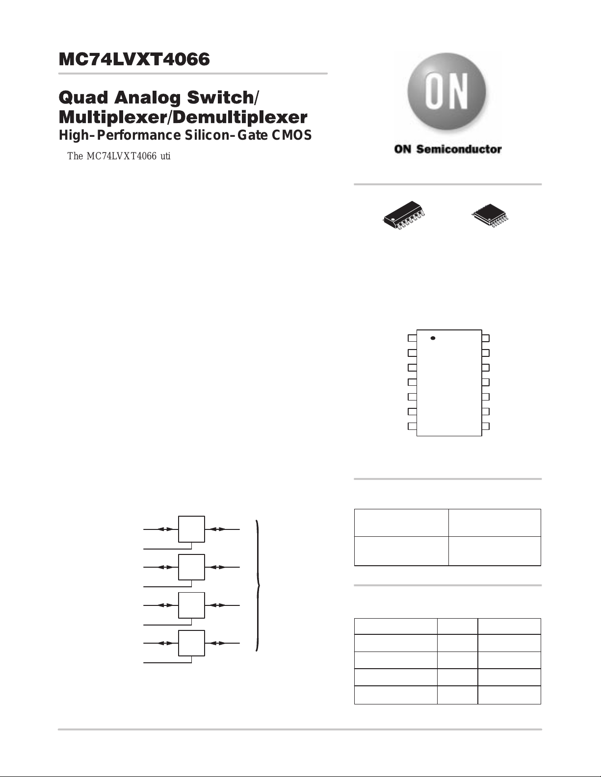
LOGIC DIAGRAM
12
X
A
A ON/OFF CONTROL
B ON/OFF CONTROL
C ON/OFF CONTROL
D ON/OFF CONTROL
ANALOG INPUTS/OUTPUTS = XA, XB, XC, X
PIN 14 = V
PIN 7 = GND
CC
13
43
X
B
5
89
X
C
6
11 10
X
D
12
D
Y
A
Y
B
ANALOG
OUTPUTS/INPUTS
Y
C
Y
D
ON
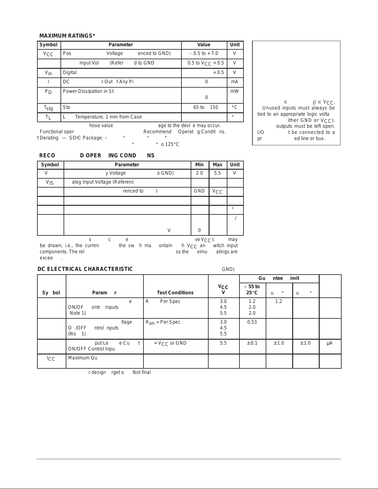
http://onsemi.com
14–LEAD SOIC
D SUFFIX
CASE 751A
14–LEAD TSSOP
DT SUFFIX
CASE 948G
PIN CONNECTION AND
MARKING DIAGRAM (Top View)
X
Y
Y
X
B ON/OFF
CONTROL
C ON/OFF
CONTROL
GND
For detailed package marking information, see the Marking
Diagram section on page 10 of this data sheet.
1
A
2
A
3
B
4
B
6
7
V
14
13
12
11
105
9
8
CC
A ON/OFF
CONTROL
D ON/OFF
CONTROL
X
D
Y
D
Y
C
X
C
FUNCTION TABLE
On/Off Control
Input
L
H
State of
Analog Switch
Off
On
ORDERING INFORMATION
Device Package Shipping
MC74L VXT4066D SOIC 55 Units/Rail
MC74L VXT4066DR2 SOIC
MC74L VXT4066DT TSSOP 96 Units/Rail
MC74L VXT4066DTR2 TSSOP
2500 Units/Reel
2500 Units/Reel
Semiconductor Components Industries, LLC, 1999
March, 2000 – Rev . 1
1 Publication Order Number:
MC74LVXT4066/D
MC74LVXT4066
ÎÎ
ÎÎ
ÎÎ
ÎÎ
ÎÎ
ÎÎ
Î
Î
Î
ÎÎ
ÎÎ
Î
Î
Î
Î
Î
Î
ÎÎÎ
Î
Î
Î
Î
Î
Î
Î
Î
Î
ÎÎÎ
Î
Î
Î
Î
Î
Î
Î
Î
Î
ÎÎÎ
Î
Î
Î
Î
Î
Î
Î
Î
Î
ÎÎÎ
Î
Î
Î
Î
ÎÎÎ
MAXIMUM RATINGS*
Symbol
V
T
Positive DC Supply Voltage (Referenced to GND)
CC
V
Analog Input Voltage (Referenced to GND)
IS
V
Digital Input Voltage (Referenced to GND)
in
I
DC Current Into or Out of Any Pin
P
Power Dissipation in Still Air, SOIC Package†
D
Storage Temperature
stg
T
Lead Temperature, 1 mm from Case for 10 Seconds
L
*Maximum Ratings are those values beyond which damage to the device may occur.
Functional operation should be restricted to the Recommended Operating Conditions.
†Derating — SOIC Package: – 7 mW/_C from 65_ to 125_C
TSSOP Package: – 6.1 mW/_C from 65_ to 125_C
RECOMMENDED OPERATING CONDITIONS
Symbol
V
V
V
VIO*
T
tr, t
ÎÎ
*For voltage drops across the switch greater than 1.2 V (switch on), excessive VCC current may
be drawn; i.e., the current out of the switch may contain both VCC and switch input
components. The reliability of the device will be unaffected unless the Maximum Ratings are
exceeded.
Positive DC Supply Voltage (Referenced to GND)
CC
Analog Input Voltage (Referenced to GND)
IS
Digital Input Voltage (Referenced to GND)
in
Static or Dynamic Voltage Across Switch
Operating Temperature, All Package Types
A
Input Rise and Fall Time, ON/OFF Control
f
Inputs (Figure 10) VCC = 3.3 V ± 0.3 V
ООООООООООООО
Parameter
Parameter
TSSOP Package†
VCC = 5.0 V ± 0.5 V
Value
– 0.5 to + 7.0
– 0.5 to VCC + 0.5
– 0.5 to VCC + 0.5
–20
500
450
– 65 to + 150
260
Min
Max
2.0
5.5
GND
V
CC
GND
V
CC
—
1.2
– 55
+ 85
0
100
Î
0
20
Unit
mA
mW
_
_
Unit
_
ns/V
Î
This device contains protection
V
V
V
circuitry to guard against damage
due to high static voltages or electric
fields. However, precautions must
be taken to avoid applications of any
voltage higher than maximum rated
voltages to this high–impedance circuit. For proper operation, Vin and
V
should be constrained to the
out
C
C
Unused inputs must always be
tied to an appropriate logic voltage
level (e.g., either GND or VCC).
range GND v (Vin or V
) v VCC.
out
Unused outputs must be left open.
I/O pins must be connected to a
properly terminated line or bus.
V
V
V
V
C
DC ELECTRICAL CHARACTERISTIC Digital Section (Voltages Referenced to GND)
V
ÎÎ
Symbol
V
ÎÎ
V
ÎÎ
ÎÎ
I
ОООООООО
Minimum High–Level Voltage
IH
ON/OFF Control Inputs
ОООООООО
(Note 1)
Maximum Low–Level Voltage
IL
ON/OFF Control Inputs
ОООООООО
(Note 1)
I
CC
Maximum Input Leakage Current
in
ОООООООО
ON/OFF Control Inputs
Maximum Quiescent Supply
Current (per Package)
Parameter
ООООО
Test Conditions
Ron = Per Spec
ООООО
Ron = Per Spec
ООООО
Vin = VCC or GND
ООООО
Vin = VCC or GND
VIO = 0 V
1. Specifications are for design target only. Not final specification limits.
CC
ÎÎÎ
V
3.0
4.5
ÎÎÎ
5.5
3.0
4.5
ÎÎÎ
5.5
5.5
ÎÎÎ
5.5
Guaranteed Limit
– 55 to
ÎÎ
25_C
1.2
2.0
ÎÎ
2.0
0.53
0.8
ÎÎ
0.8
± 0.1
ÎÎ
4.0
v
Î
85_C
1.2
2.0
Î
2.0
0.53
0.8
Î
0.8
± 1.0
Î
40
ÎÎ
v
125_C
1.2
2.0
ÎÎ
2.0
0.53
0.8
ÎÎ
0.8
± 1.0
ÎÎ
160
Î
Unit
Î
Î
µA
Î
µA
V
V
http://onsemi.com
2
MC74LVXT4066
ÎÎÎ
Î
Î
Î
Î
Î
Î
Î
Î
Î
Î
ÎÎÎ
Î
Î
Î
Î
Î
Î
Î
Î
Î
Î
Î
Î
Î
Î
Î
Î
Î
Î
ÎÎÎ
Î
Î
Î
Î
Î
Î
Î
Î
Î
Î
Î
Î
Î
ÎÎÎ
Î
Î
Î
Î
Î
Î
Î
Î
Î
Î
Î
Î
Î
Î
ÎÎÎ
Î
Î
Î
Î
Î
Î
Î
Î
Î
Î
Î
Î
Î
ÎÎÎ
Î
Î
Î
Î
Î
Î
Î
Î
ÎÎÎ
Î
Î
Î
Î
Î
Î
Î
Î
Î
Î
Î
Î
ÎÎÎ
Î
Î
Î
Î
Î
Î
Î
Î
Î
Î
Î
Î
Î
Î
Î
Î
ÎÎÎ
Î
Î
Î
Î
Î
Î
Î
Î
Î
Î
Î
Î
Î
Î
Î
Î
ÎÎÎ
Î
Î
Î
Î
Î
Î
Î
Î
ÎÎÎ
Î
Î
Î
ÎÎÎ
Î
Î
Î
Î
DC ELECTRICAL CHARACTERISTICS Analog Section (Voltages Referenced to GND)
Guaranteed Limit
V
Symbol
R
on
ÎÎ
ÎÎ
ÎÎ
ÎÎ
∆R
on
ÎÎ
I
off
ÎÎ
ÎÎ
I
on
ÎÎ
Maximum “ON” Resistance
ОООООООО
ОООООООО
ОООООООО
ОООООООО
Maximum Difference in “ON”
Resistance Between Any Two
ОООООООО
Channels in the Same Package
Maximum Off–Channel Leakage
ОООООООО
Current, Any One Channel
ОООООООО
Maximum On–Channel Leakage
Current, Any One Channel
ОООООООО
Parameter
Test Conditions
Vin = V
IH
ОООООО
VIS = VCC to GND
IS v 2.0 mA (Figures 1, 2)
ОООООО
Vin = V
IH
VIS = VCC or GND (Endpoints)
ОООООО
IS v 2.0 mA (Figures 1, 2)
ОООООО
Vin = V
IH
VIS = 1/2 (VCC – GND)
ОООООО
IS v 2.0 mA
Vin = V
IL
ОООООО
VIO = VCC or GND
Switch Off (Figure 3)
ОООООО
Vin = V
IH
VIS = VCC or GND
(Figure 4)
ОООООО
2.0†
ÎÎ
3.0
4.5
ÎÎ
5.5
2.0
3.0
ÎÎ
4.5
ÎÎ
5.5
3.0
4.5
ÎÎ
5.5
5.5
ÎÎ
ÎÎ
5.5
ÎÎ
†At supply voltage (VCC) approaching 2 V the analog switch–on resistance becomes extremely non–linear. Therefore, for low–voltage
operation, it is recommended that these devices only be used to control digital signals.
CC
V
– 55 to
25_C
—
ÎÎ
40
25
ÎÎ
20
—
30
ÎÎ
25
ÎÎ
20
15
10
ÎÎ
10
0.1
ÎÎ
ÎÎ
0.1
ÎÎ
v
85_C
—
Î
45
28
Î
25
—
35
Î
28
Î
25
20
12
Î
12
0.5
Î
Î
0.5
Î
v
125_C
—
ÎÎ
50
35
ÎÎ
30
—
40
ÎÎ
35
ÎÎ
30
25
15
ÎÎ
15
1.0
ÎÎ
ÎÎ
1.0
ÎÎ
Unit
Ω
Î
Î
Î
Î
Ω
Î
µA
Î
Î
µA
Î
AC ELECTRICAL CHARACTERISTICS (C
ÎÎÎ
Symbol
t
,
PLH
t
PHL
ÎÎÎ
ÎÎÎ
t
,
PLZ
t
PHZ
ÎÎÎ
ÎÎÎ
t
,
PZL
t
PZH
ÎÎÎ
ÎÎÎ
C
ОООООООООООООО
Maximum Propagation Delay , Analog Input to Analog Output
(Figures 8 and 9)
ОООООООООООООО
ОООООООООООООО
Maximum Propagation Delay, ON/OFF Control to Analog Output
(Figures 10 and 11)
ОООООООООООООО
ОООООООООООООО
Maximum Propagation Delay, ON/OFF Control to Analog Output
(Figures 10 and 1 1)
ОООООООООООООО
ОООООООООООООО
Maximum Capacitance ON/OFF Control Input
= 50 pF, ON/OFF Control Inputs: tr = tf = 6 ns)
L
Parameter
Control Input = GND
Analog I/O
ÎÎÎÎОООООООООООООО
C
PD
Power Dissipation Capacitance (Per Switch) (Figure 13)*
Feedthrough
*Used to determine the no–load dynamic power consumption: PD = CPD V
ÎÎ
ÎÎ
ÎÎ
ÎÎ
ÎÎ
ÎÎ
ÎÎ
ÎÎ
2
f + ICC VCC.
CC
Guaranteed Limit
V
2.0
3.0
4.5
5.5
2.0
3.0
4.5
5.5
2.0
3.0
4.5
5.5
—
—
—
CC
V
– 55 to
ÎÎ
25_C
4.0
3.0
ÎÎ
1.0
ÎÎ
1.0
30
20
ÎÎ
15
15
ÎÎ
20
12
ÎÎ
8.0
8.0
ÎÎ
10
35
1.0
ÎÎ
v
Î
85_C
6.0
5.0
Î
2.0
Î
2.0
35
25
Î
18
18
Î
25
14
Î
10
10
Î
10
35
1.0
Î
ÎÎ
v
125_C
8.0
6.0
ÎÎ
2.0
ÎÎ
2.0
40
30
ÎÎ
22
20
ÎÎ
30
15
ÎÎ
12
12
ÎÎ
10
35
1.0
ÎÎ
Î
Unit
Î
Î
Î
Î
Î
Î
pF
Î
ns
ns
ns
Typical @ 25°C, VCC = 5.0 V
15
pF
http://onsemi.com
3
MC74LVXT4066
Î
Î
Î
Î
Î
Î
Î
Î
Î
Î
Î
Î
Î
Î
Î
Î
Î
Î
Î
Î
Î
Î
Î
Î
Î
Î
Î
Î
Î
Î
Î
Î
Î
Î
Î
Î
Î
Î
Î
Î
Î
Î
Î
Î
Î
Î
Î
Î
Î
Î
Î
Î
Î
Î
Î
Î
Î
Î
Î
Î
ADDITIONAL APPLICATION CHARACTERISTICS (Voltages Referenced to GND Unless Noted)
Symbol
ÎÎ
BW
ОООООООО
Maximum On–Channel Bandwidth
or Minimum Frequency Response
ÎÎ
—
ÎÎ
ÎÎ
—
ÎÎ
ÎÎ
—
ÎÎ
ÎÎ
THD
ÎÎ
ÎÎ
(Figure 5)
ОООООООО
Off–Channel Feedthrough Isolation
ОООООООО
(Figure 6)
ОООООООО
Feedthrough Noise, Control to
ОООООООО
Switch
(Figure 7)
ОООООООО
Crosstalk Between Any Two
ОООООООО
Switches
(Figure 12)
ОООООООО
Total Harmonic Distortion
ОООООООО
(Figure 14)
ОООООООО
*Guaranteed limits not tested. Determined by design and verified by qualification.
Parameter
ОООООООООООО
Test Conditions
fin = 1 MHz Sine Wave
Adjust fin Voltage to Obtain 0 dBm at V
Increase fin Frequency Until dB Meter Reads – 3 dB
ОООООООООООО
OS
RL = 50 Ω, CL = 10 pF
fin Sine Wave
ОООООООООООО
Adjust fin Voltage to Obtain 0 dBm at V
ОООООООООООО
fin = 10 kHz, RL = 600 Ω, CL = 50 pF
IS
fin = 1.0 MHz, RL = 50 Ω, CL = 10 pF
Vin v 1 MHz Square Wave (tr = tf = 3 ns)
ОООООООООООО
Adjust RL at Setup so that IS = 0 A
ОООООООООООО
RL = 600 Ω, CL = 50 pF
RL = 10 kΩ, CL = 10 pF
fin Sine Wave
ОООООООООООО
Adjust fin Voltage to Obtain 0 dBm at V
ОООООООООООО
fin = 10 kHz, RL = 600 Ω, CL = 50 pF
IS
fin = 1.0 MHz, RL = 50 Ω, CL = 10 pF
fin = 1 kHz, RL = 10 kΩ, CL = 50 pF
ОООООООООООО
THD = THD
ОООООООООООО
Measured
– THD
Source
VIS = 4.0 VPP sine wave
VIS = 5.0 VPP sine wave
V
CC
Î
4.5
5.5
Î
4.5
Î
5.5
Î
4.5
5.5
4.5
Î
5.5
Î
4.5
5.5
4.5
Î
5.5
Î
4.5
5.5
Î
4.5
Î
5.5
V
25_C
ÎÎ
150
Unit
Î
MHz
160
Limit*
ÎÎ
– 50
ÎÎ
– 50
ÎÎ
Î
dB
Î
Î
– 37
– 37
100
ÎÎ
200
ÎÎ
mV
Î
Î
PP
50
100
– 70
ÎÎ
– 70
ÎÎ
dB
Î
Î
– 80
– 80
ÎÎ
0.10
ÎÎ
Î
Î
%
0.06
http://onsemi.com
4
 Loading...