


Motorola MC74LVXC3245DT, MC74LVXC3245DW Datasheet
SEMICONDUCTOR TECHNICAL DATA
# # #&
" !$
%" "" #"#"! &!"!
The 74LVXC3245 is a 24–pin dual–supply, octal configurable voltage
interface transceiver especially well suited for PCMCIA and other real
time configurable I/O applications. The V
level; the A port is a dedicated 3V port. The V
supply level. The B port is configured to track the V
level on the V
V
will configure the I/O pins at a 3V level. The A port interfaces with a
CCB
3V host system and the B port to the card slots. This device will allow the
V
voltage source pin and I/O pins on the B port to float when OE
CCB
High. This feature is necessary to buffer data to and from a PCMCIA
socket that permits PCMCIA cards to be inserted and removed during
normal operation. The Transmit/Receive (T/R
direction of data flow. T ransmit (active–High) enables data from the A port
to B port. Receive (active–Low) enables data from the B port to the A port.
pin will configure the I/O pins at a 5V level and a 3V
CCB
• Bidirectional Interface Between 3V and 3V/5V Buses
• Control Inputs Compatible with TTL Level
• Outputs Source/Sink Up to 24mA
• Guaranteed Simultaneous Switching Noise Level and Dynamic
Threshold Performance
• Available in SOIC and TSSOP Packages
• Flexible V
• Allows B Port and V
Operating Range
CCB
CCB
to Float Simultaneously When OE Is High
• Functionally Compatible with the 74 Series 245
pin accepts a 3V supply
CCA
pin accepts a 3V–to–5V
CCB
supply level. A 5V
CCB
) input determines the
is
LVX
LOW–VOLTAGE CMOS
DW SUFFIX
24–LEAD PLASTIC WIDE SOIC PACKAGE
CASE 751E–04
DT SUFFIX
24–LEAD PLASTIC TSSOP PACKAGE
CASE 948H–01
V
NC OE
CCB
2324 22 21 20 19 18
21 34567
V
T/R
CCA
This document contains information on a new product. Specifications and information herein are subject to
change without notice.
7/97
Motorola, Inc. 1997
B0 B1 B2 B3 B4 B5 B6
16
17
9
8
A0 A1 A2 A3 A4 A5 A6 A7
Figure 1. 24–Lead Pinout (Top View)
1
15
10
B7 GND
14
13
11
12
GND GND
PIN NAMES
Pins
OE
T/R
A0–A7
B0–B7
REV 1
Function
Output Enable Input
Transmit/Receive Input
Side A 3–State Inputs or 3–State
Outputs
Side B 3–State Inputs or 3–State
Outputs
MC74LVXC3245
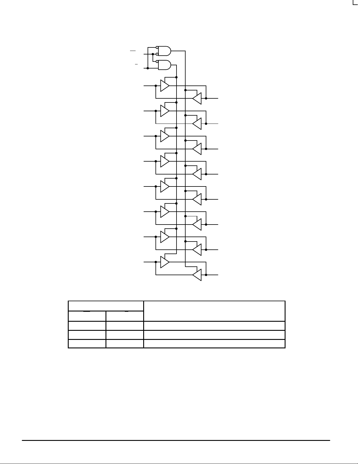
OPERATING MODE
OE
T/R 2
22
A0
A1
A2
A3
A4
A5
A6
A7
10
3
21
B0
4
20
B1
5
19
B2
6
18
B3
7
17
B4
8
16
B5
9
15
B6
14
B7
Figure 2. Logic Diagram
INPUTS
OE T/R
L L B Data to A Bus
L H A Data to B Bus
H X Z
H = High Voltage Level; L = Low V oltage Level; Z = High Impedance State; X = High or Low Voltage Level
and Transitions are Acceptable; For ICC reasons, Do Not Float Inputs
MOTOROLA LVX Data — Low–Voltage CMOS Logic
2
Non–Inverting
BR1492 — Rev 0
MC74LVXC3245
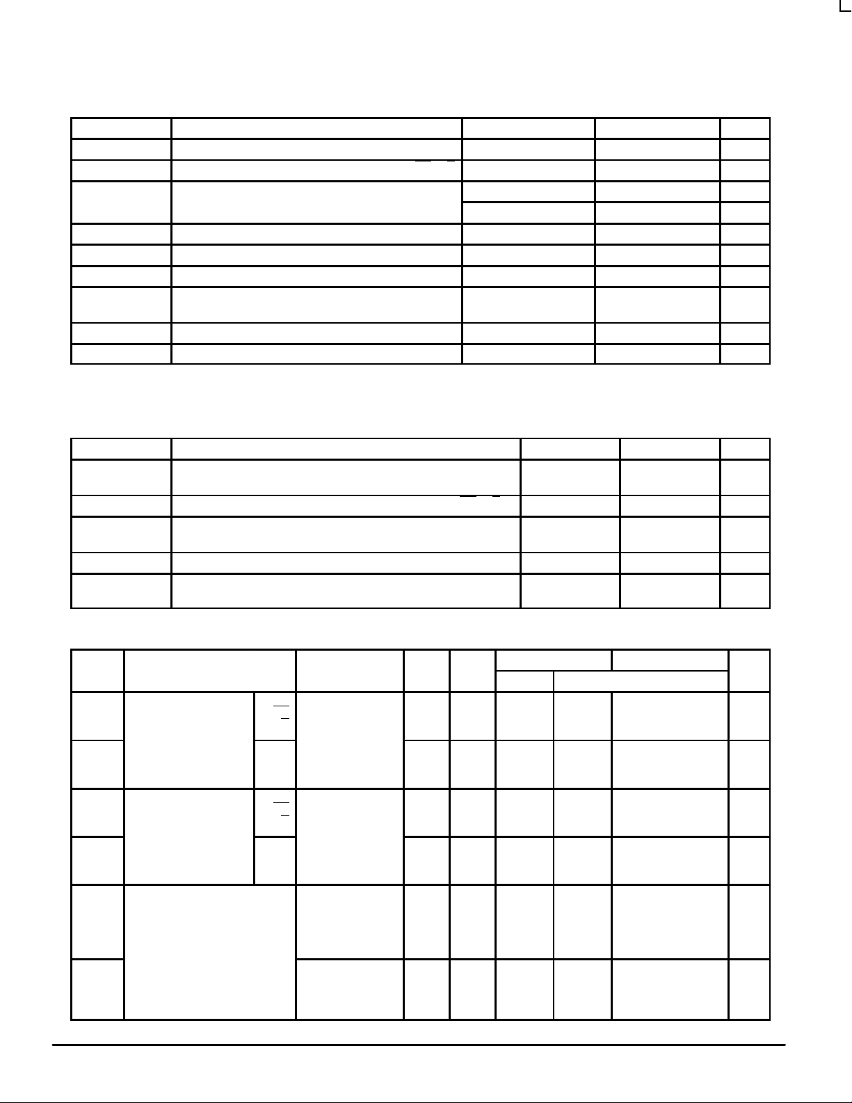
ABSOLUTE MAXIMUM RATINGS*
Symbol Parameter Value Condition Unit
V
, V
CCA
CCB
V
I
V
I/O
I
IK
I
OK
I
O
ICC, I
GND
T
STG
* Absolute maximum continuous ratings are those values beyond which damage to the device may occur. Exposure to these conditions or conditions
beyond those indicated may adversely affect device reliability. Functional operation under absolute–maximum–rated conditions is not implied.
RECOMMENDED OPERATING CONDITIONS
Symbol Parameter Min Max Unit
V
, V
CCA
CCB
V
I
V
I/O
T
A
∆t/∆V Minimum Input Edge Rate
DC Supply Voltage –0.5 to +7.0 V
DC Input Voltage OE, T/R –0.5 to V
DC Input/Output Voltage An –0.5 to V
Bn –0.5 to V
DC Input Diode Current OE, T/R ±20 VI < GND mA
DC Output Diode Current ±50 VO < GND; VO > V
DC Output Source/Sink Current ±50 mA
DC Supply Current Per Output Pin
Storage Temperature Range –65 to +150 °C
DC Latchup Source/Sink Current ±300 mA
Supply Voltage (V
Input Voltage OE, T/R 0 V
Input/Output Voltage An
Operating Free–Air Temperature –40 +85 °C
VIN from 30% to 70% of VCC; VCC at 3.0V , 4.5V, 5.5V
CCA
≤ V
CCB
Maximum Current
)V
V
CCA
CCB
Bn
+0.5 V
CCA
+0.5 V
CCA
+0.5 V
CCB
±50
±200
2.7
3.0
0
0
0 8 ns/V
V
V
3.6
5.5
CCA
CCA
CCB
CC
mA
mA
V
V
V
DC ELECTRICAL CHARACTERISTICS
Symbol Parameter Condition V
V
V
V
V
V
V
IHA
IHB
ILA
ILB
OHA
OHB
Minimum HIGH Level
Input Voltage
Maximum LOW Level
Input Voltage
Minimum HIGH Level
Output Voltage
An
OE
T/R
Bn
An
OE
T/R
Bn
V
≤ 0.1V
OUT
or
≥ VCC – 0.1V
V
≤ 0.1V
OUT
or
≥ VCC – 0.1V
I
= –100µA
OUT
IOH = –12mA
IOH = –24mA
IOH = –12mA
IOH = –24mA
I
= –100µA
OUT
IOH = –12mA
IOH = –24mA
IOH = –24mA
CCAVCCB
2.7
3.0
3.6
2.7
3.0
3.6
2.7
3.0
3.6
2.7
3.0
3.6
3.0
3.0
3.0
2.7
2.7
3.0
3.0
3.0
3.0
3.0
3.6
5.5
3.0
3.6
5.5
3.0
3.6
5.5
3.0
3.6
5.5
3.0
3.0
3.0
3.0
4.5
3.0
3.0
3.0
4.5
TA = 25°C TA = –40 to +85°C
Typ Guaranteed Limits Unit
2.99
2.85
2.65
2.50
2.30
2.99
2.85
2.65
4.25
2.0
2.0
2.0
2.00
2.00
3.85
0.8
0.8
0.8
0.80
0.80
1.65
2.90
2.56
2.35
2.30
2.10
2.90
2.56
2.35
3.86
2.0
2.0
2.0
2.00
2.00
3.85
0.8
0.8
0.8
0.80
0.80
1.65
2.90
2.46
2.25
2.20
2.00
2.90
2.46
2.25
3.76
V
V
V
V
V
V
LVX Data — Low–Voltage CMOS Logic
BR1492 — Rev 0
3 MOTOROLA
 Loading...