


 Loading...
Mitsubishi M38027M8DXXXSP, M38027M8DXXXFP, M38027E8DXXXSP, M38027E8DXXXFP, M38027E8DSP Datasheet
...ADVANCED AND EVER ADVANCING MITSUBISHI ELECTRIC
MITSUBISHI 8-BIT SINGLE-CHIP MICROCOMPUTER
740 FAMILY / 38000 SERIES
3802
Group
User’s Manual
MITSUBISHI
ELECTRIC

keep safety first in your circuit designs !
●Mitsubishi Electric Corporation puts the maximum effort into making semiconductor products better and more reliable, but there is always the possibility that trouble may occur with them. Trouble with semiconductors may lead to personal injury, fire or property damage. Remember to give due consideration to safety when making your circuit designs, with appropriate measures such as (i) placement of substitutive, auxiliary circuits, (ii) use of non-flammable material or (iii) prevention against any malfunction or mishap.
Notes regarding these materials
●These materials are intended as a reference to assist our customers in the selection of the Mitsubishi semiconductor product best suited to the customer’s application; they do not convey any license under any intellectual property rights, or any other rights, belonging to Mitsubishi Electric Corporation or a third party.
●Mitsubishi Electric Corporation assumes no responsibility for any damage, or infringement of any third-party’s rights, originating in the use of any product data, diagrams, charts or circuit application examples contained in these materials.
●All information contained in these materials, including product data, diagrams and charts, represent information on products at the time of publication of these materials, and are subject to change by Mitsubishi Electric Corporation without notice due to product improvements or other reasons. It is therefore recommended that customers contact Mitsubishi Electric Corporation or an authorized Mitsubishi Semiconductor product distributor for the latest product information before purchasing a product listed herein.
●Mitsubishi Electric Corporation semiconductors are not designed or manufactured for use in a device or system that is used under circumstances in which human life is potentially at stake. Please contact Mitsubishi Electric Corporation or an authorized Mitsubishi Semiconductor product distributor when considering the use of a product contained herein for any specific purposes, such as apparatus or systems for transportation, vehicular, medical, aerospace, nuclear, or undersea repeater use.
●The prior written approval of Mitsubishi Electric Corporation is necessary to reprint or reproduce in whole or in part these materials.
●If these products or technologies are subject to the Japanese export control restrictions, they must be exported under a license from the Japanese government and cannot be imported into a country other than the approved destination.
Any diversion or reexport contrary to the export control laws and regulations of Japan and/or the country of destination is prohibited.
●Please contact Mitsubishi Electric Corporation or an authorized Mitsubishi Semiconductor product distributor for further details on these materials or the products contained therein.
Preface
This user’s manual describes Mitsubishi’s CMOS 8- bit microcomputers 3802 Group.
After reading this manual, the user should have a through knowledge of the functions and features of the 3802 Group, and should be able to fully utilize the product. The manual starts with specifications and ends with application examples.
For details of software, refer to the “SERIES MELPS 740 <SOFTWARE> USER’S MANUAL.”
For details of development support tools, refer to the “DEVELOPMENT SUPPORT TOOLS FOR MICROCOMPUTERS” data book.
BEFORE USING THIS USER’S MANUAL
This user’s manual consists of the following three chapters. Refer to the chapter appropriate to your conditions, such as hardware design or software development. Chapter 3 also includes necessary information for systems development. Be sure to refer to this chapter.
1.Organization
●CHAPTER 1 HARDWARE
This chapter describes features of the microcomputer and operation of each peripheral function.
●CHAPTER 2 APPLICATION
This chapter describes usage and application examples of peripheral functions, based mainly on setting examples of related registers.
●CHAPTER 3 APPENDIX
This chapter includes necessary information for systems development using the microcomputer, electric characteristics, a list of registers, the masking confirmation (mask ROM version), and mark specifications which are to be submitted when ordering.
2.Structure of register
The figure of each register structure describes its functions, contents at reset, and attributes as follows :
|
|
|
|
|
|
|
|
|
|
|
(Note 2) |
|
|
|
|
|
|
|
|
|
Bits |
Bit attributes |
|
|
|
|
|
|
|
|
|
|
|
(Note 1) |
|
b7 b6 b5 b4 b3 b2 b1 b0 |
|
Contents immediately after reset release |
|||||||||
|
|
|
|
||||||||
|
|
0 |
|
|
|
|
|
|
|
|
|
|
|
|
|
|
|
|
|
CPU mode register (CPUM) [Address : 3B16] |
|
|
|
|
|
|
|
|
|
|
|
|
|
|
|
B |
Name |
|
|
Function |
|
At reset |
R |
W |
0 |
Processor mode bits |
b1 b0 |
|
|
0 |
|
|
|
0 |
0 : Single-chip mode |
|
|
|||||
|
|
0 1 : |
Not available |
|
|
|
|
|
1 |
|
1 0 : |
|
0 |
|
|
||
|
1 1 : |
|
|
|
|
|||
2 |
Stack page selection bit |
0 : 0 page |
|
0 |
|
|
||
1 : 1 page |
|
|
|
|||||
3 |
Nothing arranged for these bits. These are write disabled |
0 |
|
|
||||
4 |
bits. When these bits are read out, the contents are |
“0.” |
0 |
|
|
|||
|
|
|
|
|
|
|||
5 |
Fix this bit to “0.” |
|
|
|
|
1 |
|
|
6 |
Main clock (XIN-XOUT) stop bit |
0 : Operating |
|
|
|
|
||
1 |
: Stopped |
|
|
|
||||
7 |
Internal system clock selection bit |
0 |
: XIN-XOUT selected |
|
|
|
|
|
1 |
: XCIN-XCOUT selected |
|
|
|||||
: Bit in which nothing is arranged |
: Bit that is not used for control of the corresponding function |
Note 1. Contents immediately after reset release 0••••••“0” at reset release 1••••••“1” at reset release
Undefined••••••Undefined or reset release
••••••Contents determined by option at reset release
Note 2. Bit attributes••••••The attributes of control register bits are classified into 3 bytes : read-only, write-only and read and write. In the figure, these attributes are represented as follows :
R••••••Read |
W••••••Write |
••••••Read enabled |
••••••Write enabled |
••••••Read disabled |
••••••Write disabled |

LIST OF GROUPS HAVING THE SIMILAR FUNCTIONS
3802 group, one of the CMOS 8-bit microcomputer 38000 series presented in this user’s manual is provided with standard functions.
The basic functions of the 3800, 3802, 3806 and 3807 groups having the same functions are shown below. For the detailed functions of each group, refer to the related data book and user’s manual.
List of groups having the same functions
As of September 1995
Group |
3800 group |
3802 group |
3806 group |
3807 group |
|
Function |
|||||
|
|
|
|
Pin (Package type)
Clock generating circuit
Timer
Serial I/O
A-D converter
D-A converter
Mask
ROM
One Time
Memory PROM
type
EPROM
RAM
Remarks
64 pin |
64 pin |
80 pin |
80 pin |
• 64P4B |
• 64P4B |
• 80P6N-A |
• 80P6N-A |
• 64P6N-A |
• 64P6N-A |
• 80P6S-A |
|
• 64P6D-A |
|
• 80P6D-A |
|
|
|
|
|
|
|
|
|
1 circuit |
|
|
|
|
|
|
|
1 circuit |
|
|
|
|
|
|
1 circuit |
|
|
2 circuit |
|
||||||||||||||
|
|
|
|
|
|
|
|
|
|
|
|
|
|
|
|
|
|
|
|
|
|
|
|
|
|
|
|
|
|
|
|
|
|
|
|
|
|
|
|
|
|
|
|
|
|
|
|
|
|
|
|
|
|
|
|
|
|
|
|
|
|
|
|
|
|
|
|
|
|
|
|
|
|
<8-bit> |
|
|
|
|
|
<8-bit> |
|
|
|
|
|
|
|
<8-bit> |
|
|
|
|
|
|
|
<8-bit> |
|
|
Timer : 3 |
|
|||||||||||||
|
|
|
|
Prescaler : 3 |
|
|
|
|
|
|
Prescaler : 3 |
|
|
|
|
|
Prescaler : 3 |
|
|
<16-bit> |
|
||||||||||||||||
|
|
|
|
Timer : 4 |
|
|
|
|
|
|
Timer : 4 |
|
|
|
|
|
Timer : 4 |
|
|
Timer X/Y : 2 |
|
||||||||||||||||
|
|
|
|
|
|
|
|
|
|
|
|
|
|
|
|
|
|
|
|
|
|
|
|
|
|
|
|
|
|
|
|
|
|
|
|
|
|
|
|
|
|
|
|
|
|
|
|
|
|
|
|
|
|
|
|
|
|
|
|
|
|
|
|
|
|
|
|
|
|
|
|
|
|
Timer A/B : 2 |
|
|
|
UART or |
|
|
|
|
|
|
|
|
UART or |
|
|
|
|
|
UART or |
|
|
|
|
|
|
|
UART or |
|
|||||||||||
|
|
Clock synchronous 1 |
Clock synchronous 1 |
|
Clock synchronous 1 |
|
Clock synchronous 1 |
|
|||||||||||||||||||||||||||||
|
|
|
|
|
|
|
|
|
|
|
|
|
Clock synchronous 1 |
|
Clock synchronous 1 |
|
Clock synchronous 1 |
|
|||||||||||||||||||
|
|
|
|
|
|
|
|
|
|
|
|
|
|
|
|
||||||||||||||||||||||
|
|
|
|
|
|
|
|
|
|
|
|
|
|
|
|
||||||||||||||||||||||
|
|
|
|
|
|
|
|
|
|
|
|
|
|
|
|
|
|
|
|
|
|
|
|
|
|
|
|
|
|
|
|
|
|
||||
|
|
|
|
|
|
|
|
|
|
|
|
|
|
|
8-bit 8-channel |
|
|
|
8-bit 8-channel |
|
|
8-bit 13-channel |
|
||||||||||||||
|
|
|
|
|
|
|
|
|
|
|
|
|
|
|
|
|
|
|
|||||||||||||||||||
|
|
|
|
|
|
|
|
|
|
|
|
|
|
|
8-bit 2-channel |
|
|
|
|
|
|
|
|
|
|
|
|
|
|||||||||
|
|
|
|
|
|
|
|
|
|
|
|
|
|
|
|
|
|
8-bit 2-channel |
|
8-bit 4-channel |
|
||||||||||||||||
|
|
|
|
|
|
|
|
|
|
|
|
|
|
|
|
|
|
||||||||||||||||||||
|
|
|
|
|
|
|
|
|
|
|
|
|
|
|
|
|
|
|
|
|
|
|
|
|
|
|
|
|
|
|
|
|
|
||||
|
8K |
16K 24K 32K |
|
|
8K |
16K |
24K |
32K |
12K 16K 24K 32K 48K |
|
16K |
|
|||||||||||||||||||||||||
|
(Note 1) |
(Note 1) |
|
|
|
|
(Note 1) |
|
|
|
(Note 1) |
(Note 1) |
|
|
|
(Note 1) |
(Note 1) |
(Note 1) |
(Note 3) (Note 3) |
(Note 3) |
|
|
|
||||||||||||||
|
|
|
|
|
|
|
|
|
|
|
|
|
|
|
|
|
|
|
|
|
|
|
|
|
|
|
|
|
|
|
|
|
|
|
|
|
|
|
8K |
16K |
|
|
|
|
32K |
|
|
|
|
|
|
|
|
|
|
|
|
32K |
|
|
|
|
|
|
24K |
|
|
48K |
|
16K |
|
||||
|
|
|
|
|
|
|
|
|
|
|
|
|
|
|
|
|
|
|
|
|
|
|
|
|
|
||||||||||||
|
|
|
|
(Note 1) |
|
|
|
|
|
|
|
|
|
|
|
|
|
|
|
|
|
(Note 1) |
|
|
|
|
|
|
(Note 2) |
(Note 3) |
|
|
|
||||
|
|
|
|
16K |
|
|
|
|
32K |
|
|
|
|
|
|
|
|
|
|
|
|
32K |
|
|
|
|
|
|
24K |
|
|
|
48K |
|
16K |
|
|
|
|
|
|
|
|
|
|
|
|
|
|
|
|
|
|
|
|
|
|
|
|
|
|
|
|
|
|
|
|
|
|||||||
|
|
|
|
|
|
|
|
|
|
|
|
|
|
|
|
|
|
|
|
|
|
|
|
|
|
|
|
|
(Note 2) |
|
|
||||||
|
|
|
|
|
|
|
|
|
|
|
|
|
|
|
|
|
|
|
|
|
|
|
|
|
|
|
|
|
|
|
|
|
|
|
|
|
|
|
384 |
384 |
512 |
640 |
384 |
384 |
384 |
640 |
1024 |
|
|
|
384 |
512 1024 1024 |
|
512 |
|
||||||||||||||||||||
|
384 |
|
|
||||||||||||||||||||||||||||||||||
|
|
|
|
|
|
|
|
|
|
|
|
|
PWM output |
|
|
|
|
|
|
|
|
|
|
|
|
|
|
|
|
|
|
|
|||||
|
|
|
|
|
|
|
|
|
|
|
|
|
|
|
|
|
|
|
|
|
|
|
|
|
|
|
|
|
|
Real time port output |
|
||||||
|
|
|
|
|
|
|
|
|
|
|
|
|
|
|
|
|
|
|
|
|
|
|
|
|
|
|
|
|
|
|
|
|
|
|
|
Analog comparator |
|
|
|
|
|
|
|
|
|
|
|
|
|
|
|
|
|
|
|
|
|
|
|
|
|
|
|
|
|
|
|
|
|
|
|
|
|
Watchdog timer |
|
|
|
|
|
|
|
|
|
|
|
|
|
|
|
|
|
|
|
|
|
|
|
|
|
|
|
|
|
|
|
|
|
|
|
|
|
|
|
Notes 1: Extended operating temperature version available
2:High-speed version available
3:Extended operating temperature version and High-speed version available. ROM expansion

Table of contents
Table of contents
CHAPTER 1. HARDWARE
DESCRIPTION ................................................................................................................................ |
1-2 |
FEATURES ...................................................................................................................................... |
1-2 |
APPLICATIONS .............................................................................................................................. |
1-2 |
PIN CONFIGURATION ................................................................................................................... |
1-2 |
FUNCTIONAL BLOCK ................................................................................................................... |
1-4 |
PIN DESCRIPTION ......................................................................................................................... |
1-5 |
PART NUMBERING ....................................................................................................................... |
1-6 |
GROUP EXPANSION ..................................................................................................................... |
1-7 |
GROUP EXPANSION (EXTENDED OPERATING TEMPERATURE VERSION) .................... |
1-8 |
FUNCTIONAL DESCRIPTION ....................................................................................................... |
1-9 |
Central Processing Unit (CPU) ............................................................................................... |
1-9 |
Memory .................................................................................................................................... |
1-13 |
I/O Ports .................................................................................................................................. |
1-15 |
Interrupts .................................................................................................................................. |
1-18 |
Timers ...................................................................................................................................... |
1-20 |
Serial I/O.................................................................................................................................. |
1-22 |
Pulse Width Modulation (PWM) ............................................................................................ |
1-28 |
A-D Converter ......................................................................................................................... |
1-30 |
D-A Converter ......................................................................................................................... |
1-31 |
Reset Circuit ............................................................................................................................ |
1-32 |
Clock Generating Circuit ........................................................................................................ |
1-34 |
Processor Modes .................................................................................................................... |
1-35 |
NOTES ON PROGRAMMING ..................................................................................................... |
1-37 |
Processor Status Register ..................................................................................................... |
1-37 |
Interrupts .................................................................................................................................. |
1-37 |
Decimal Calculations .............................................................................................................. |
1-37 |
Timers ...................................................................................................................................... |
1-37 |
Multiplication and Division Instructions ................................................................................ |
1-37 |
Ports ......................................................................................................................................... |
1-37 |
Serial I/O.................................................................................................................................. |
1-37 |
A-D Converter ......................................................................................................................... |
1-37 |
D-A Converter ......................................................................................................................... |
1-37 |
Instruction Execution Time .................................................................................................... |
1-37 |
Memory Expansion Mode....................................................................................................... |
1-37 |
Memory Expansion Mode and Microprocessor Mode ....................................................... |
1-37 |
DATA REQUIRED FOR MASK ORDERS ................................................................................. |
1-38 |
3802 GROUP USER'S MANUAL |
i |

Table of contents
ROM PROGRAMMING METHOD ............................................................................................... |
1-38 |
FUNCTIONAL DESCRIPTION SUPPLEMENT .......................................................................... |
1-39 |
Interrupt .................................................................................................................................... |
1-39 |
Timing After Interrupt ............................................................................................................. |
1-40 |
A-D Converter ......................................................................................................................... |
1-41 |
CHAPTER 2. APPLICATION
2.1 I/O port ..................................................................................................................................... |
2-2 |
2.1.1 Memory map of I/O port ................................................................................................ |
2-2 |
2.1.2 Related registers ............................................................................................................. |
2-3 |
2.1.3 Handling of unused pins ................................................................................................ |
2-4 |
2.2 Timer ......................................................................................................................................... |
2-5 |
2.2.1 Memory map of timer ..................................................................................................... |
2-5 |
2.2.2 Related registers ............................................................................................................. |
2-6 |
2.2.3 Timer application examples ......................................................................................... |
2-11 |
2.3 Serial I/O ................................................................................................................................ |
2-23 |
2.3.1 Memory map of serial I/O ........................................................................................... |
2-23 |
2.3.2 Related registers ........................................................................................................... |
2-24 |
2.3.3 Serial I/O connection examples .................................................................................. |
2-30 |
2.3.4 Setting of serial I/O transfer data format ................................................................. |
2-32 |
2.3.5 Serial I/O application examples .................................................................................. |
2-33 |
2.4 PWM ........................................................................................................................................ |
2-53 |
2.4.1 Memory map of PWM .................................................................................................. |
2-53 |
2.4.2 Related registers ........................................................................................................... |
2-54 |
2.4.3 PWM output circuit application example ................................................................... |
2-56 |
2.5 A-D converter ........................................................................................................................ |
2-59 |
2.5.1 Memory map of A-D conversion ................................................................................. |
2-59 |
2.5.2 Related registers ........................................................................................................... |
2-60 |
2.5.3 A-D conversion application example .......................................................................... |
2-62 |
2.6 Processor mode ................................................................................................................... |
2-64 |
2.6.1 Memory map of processor mode ................................................................................ |
2-64 |
2.6.2 Related register ............................................................................................................. |
2-64 |
2.6.3 Processor mode application examples ...................................................................... |
2-65 |
2.7 Reset ....................................................................................................................................... |
2-69 |
2.7.1 Connection example of reset IC ................................................................................. |
2-69 |
CHAPTER 3. APPENDIX 
3.1 Electrical characteristics ...................................................................................................... |
3-2 |
3.1.1 Absolute maximum ratings ............................................................................................ |
3-2 |
3.1.2 Recommended operating conditions............................................................................. |
3-2 |
3.1.3 Electrical characteristics................................................................................................. |
3-3 |
ii |
3802 GROUP USER'S MANUAL |

Table of contents
|
3.1.4 A-D converter characteristics ........................................................................................ |
|
3-3 |
||
|
3.1.5 D-A converter characteristics ........................................................................................ |
|
3-4 |
||
|
3.1.6 Timing requirements and Switching characteristics .................................................. |
3-5 |
|||
|
3.1.7 Absolute maximum ratings (Extended operating temperature version) .................. |
3-9 |
|||
|
3.1.8 Recommended operating conditions(Extended operating temperature version) .... |
3-9 |
|||
|
3.1.9 Electrical characteristics (Extended operating temperature version) .................... |
3-10 |
|||
|
3.1.10 A-D converter characteristics |
(Extended operating temperature version) ........ |
3-10 |
||
|
3.1.11 D-A converter characteristics |
(Extended operating temperature version) ........ |
3-11 |
||
|
3.1.12 Timing requirements and Switching characteristics |
|
|||
|
(Extended operating temperature version) ......................................................... |
3-12 |
|||
|
3.1.13 Timing diagram ........................................................................................................... |
|
3-14 |
||
3.2 |
Standard characteristics ..................................................................................................... |
|
3-17 |
||
|
3.2.1 Power source current characteristic examples ........................................................ |
3-17 |
|||
|
3.2.2 Port standard characteristic examples ...................................................................... |
3-18 |
|||
|
3.2.3 A-D conversion standard characteristics .................................................................. |
3-20 |
|||
|
3.2.4 D-A conversion standard characteristics .................................................................. |
3-21 |
|||
3.3 |
Notes on use......................................................................................................................... |
|
3-22 |
||
|
3.3.1 Notes on interrupts ....................................................................................................... |
|
3-22 |
||
|
3.3.2 Notes on the serial I/O1 .............................................................................................. |
|
3-22 |
||
|
3.3.3 Notes on the A-D converter ........................................................................................ |
|
3-23 |
||
|
|
|
|
|
|
|
3.3.4 Notes on the RESET pin ............................................................................................. |
|
3-24 |
||
|
3.3.5 Notes on input and output pins .................................................................................. |
|
3-24 |
||
|
3.3.6 Notes on memory expansion mode and microprocessor mode ............................ |
3-25 |
|||
|
3.3.7 Notes on built-in PROM ............................................................................................... |
|
3-26 |
||
3.4 |
Countermeasures against noise ....................................................................................... |
|
3-28 |
||
|
3.4.1 Shortest wiring length .................................................................................................. |
|
3-28 |
||
|
3.4.2 Connection of a bypass capacitor across the Vss line and the Vcc line ............ |
3-29 |
|||
|
3.4.3 Wiring to analog input pins ......................................................................................... |
|
3-30 |
||
|
3.4.4 Consideration for oscillator .......................................................................................... |
|
3-30 |
||
|
3.4.5 Setup for I/O ports ....................................................................................................... |
|
3-31 |
||
|
3.4.6 Providing of watchdog timer function by software .................................................. |
3-31 |
|||
3.5 |
List of registers .................................................................................................................... |
|
3-33 |
||
3.6 |
Mask ROM ordering method .............................................................................................. |
|
3-47 |
||
3.7 |
Mark specification form ...................................................................................................... |
|
3-61 |
||
3.8 |
Package outline .................................................................................................................... |
|
3-63 |
||
3.9 |
List of instruction codes .................................................................................................... |
|
3-65 |
||
3.10 Machine Instructions ......................................................................................................... |
|
3-66 |
|||
3.11 SFR memory map .............................................................................................................. |
|
3-76 |
|||
3.12 Pin configuration ................................................................................................................ |
|
3-77 |
|||
3802 GROUP USER'S MANUAL |
iii |
|
|
|
List of figures |
|
|
|
|
|
|
|
|
|
List of figures |
|
CHAPTER 1 HARDWARE |
|
|
||
|
|
|||
|
|
|||
Fig. 1 Pin configuration of M38022M4-XXXFP .......................................................................... |
1-2 |
|||
Fig. 2 Pin configuration of M38022M4-XXXSP .......................................................................... |
1-3 |
|||
Fig. 3 Functional block diagram ................................................................................................... |
1-4 |
|||
Fig. 4 Part numbering .................................................................................................................... |
1-6 |
|||
Fig. 5 Memory expansion plan ..................................................................................................... |
1-7 |
|||
Fig. 6 Memory expansion plan (Extended operating temperature version) .......................... |
1-8 |
|||
Fig. 7 740 Family CPU register structure ................................................................................... |
1-9 |
|||
Fig. 8 Register push and pop at interrupt generation and subroutine call ........................ |
1-10 |
|||
Fig. 9 Structure of CPU mode register ..................................................................................... |
1-11 |
|||
Fig. 10 Memory map diagram .................................................................................................... |
1-12 |
|||
Fig. 11 Memory map of special function register (SFR) ....................................................... |
1-13 |
|||
Fig. 12 Port block diagram (single-chip mode) (1) ................................................................ |
1-16 |
|||
Fig. 13 Port block diagram (single-chip mode) (2) ................................................................ |
1-17 |
|||
Fig. 14 Interrupt control............................................................................................................... |
1-18 |
|||
Fig. 15 Structure of interrupt-related registers ........................................................................ |
1-18 |
|||
Fig. 16 Structure of timer XY register ....................................................................................... |
1-19 |
|||
Fig. 17 Block diagram of timer X, timer Y, timer 1, and timer 2 ........................................ |
1-21 |
|||
Fig. 18 Block diagram of clock synchronous serial I/O1....................................................... |
1-22 |
|||
Fig. 19 Operation of clock synchronous serial I/O1 function ............................................... |
1-22 |
|||
Fig. 20 Block diagram of UART serial I/O .............................................................................. |
1-23 |
|||
Fig. 21 Operation of UART serial I/O function ....................................................................... |
1-24 |
|||
Fig. 22 Structure of serial I/O control registers ...................................................................... |
1-25 |
|||
Fig. 23 Structure of serial I/O2 control register...................................................................... |
1-26 |
|||
Fig. 24 Block diagram of serial I/O2 function ......................................................................... |
1-26 |
|||
Fig. 25 Timing of serial I/O2 function ....................................................................................... |
1-27 |
|||
Fig. 26 Timing of PWM cycle ..................................................................................................... |
1-28 |
|||
Fig. 27 Block diagram of PWM function ................................................................................... |
1-28 |
|||
Fig. 28 Structure of PWM control register............................................................................... |
1-29 |
|||
Fig. 29 PWM output timing when PWM register or PWM prescaler is changed ............... |
1-29 |
|||
Fig. 30 Structure of AD/DA control register ............................................................................ |
1-30 |
|||
Fig. 31 Block diagram of A-D converter ................................................................................... |
1-30 |
|||
Fig. 32 Block diagram of D-A converter ................................................................................... |
1-31 |
|||
Fig. 33 Equivalent connection circuit of D-A converter ......................................................... |
1-31 |
|||
Fig. 34 Example of reset circuit ................................................................................................. |
1-32 |
|||
Fig. 35 Internal status of microcomputer after reset ............................................................. |
1-32 |
|||
Fig. 36 Timing of reset ................................................................................................................ |
1-33 |
|||
Fig. 37 Ceramic resonator circuit............................................................................................... |
1-34 |
|||
Fig. 38 External clock input circuit ............................................................................................ |
1-34 |
|||
Fig. 39 Block diagram of clock generating circuit .................................................................................. |
1-34 |
|||
Fig. 40 Memory maps in various processor modes ............................................................... |
1-35 |
|||
Fig. 41 Structure of CPU mode register ................................................................................... |
1-35 |
|||
|
|
|
|
|
Fig. 42 ONW function timing ...................................................................................................... |
1-36 |
|||
Fig. 43 Programming and testing of One Time PROM version ........................................... |
1-38 |
|||
Fig. 44 Timing chart after an interrupt occurs ........................................................................ |
1-40 |
|||
Fig. 45 Time up to execution of the interrupt processing routine ....................................... |
1-40 |
|||
Fig. 46 A-D conversion equivalent circuit ................................................................................. |
1-42 |
|||
Fig. 47 A-D conversion timing chart .......................................................................................... |
1-42 |
|||
|
|
|
|
|
3802 GROUP USER’S MANUAL |
i |

List of figures
CHAPTER 2 APPLICATION
Fig. 2.1.1 Memory map of I/O port related registers ............................................................... |
2-2 |
Fig. 2.1.2 Structure of Port Pi (i=0, 1, 2, 3, 4, 5, 6)............................................................... |
2-3 |
Fig. 2.1.3 Structure of Port Pi direction register (i=0, 1, 2, 3, 4, 5, 6) ................................ |
2-3 |
Fig. 2.2.1 Memory map of timer related registers ...................................................................... |
2-5 |
Fig. 2.2.2 Structure of Prescaler 12, Prescaler X, Prescaler Y .............................................. |
2-6 |
Fig. 2.2.3 Structure of Timer 1 ..................................................................................................... |
2-6 |
Fig. 2.2.4 Structure of Timer 2, Timer X, Timer Y .................................................................... |
2-7 |
Fig. 2.2.5 Structure of Timer XY mode register ......................................................................... |
2-8 |
Fig. 2.2.6 Structure of Interrupt request register 1 .................................................................... |
2-9 |
Fig. 2.2.7 Structure of Interrupt request register 2 .................................................................... |
2-9 |
Fig. 2.2.8 Structure of Interrupt control register 1 .................................................................. |
2-10 |
Fig. 2.2.9 Structure of Interrupt control register 2 .................................................................. |
2-10 |
Fig. 2.2.10 Connection of timers and setting of division ratios [Clock function] ................ |
2-12 |
Fig. 2.2.11 Setting of related registers [Clock function] ......................................................... |
2-13 |
Fig. 2.2.12 Control procedure [Clock function] ........................................................................ |
2-14 |
Fig. 2.2.13 Example of a peripheral circuit ............................................................................... |
2-15 |
Fig. 2.2.14 Connection of the timer and setting of the division ratio [Piezoelectric buzzer output] ........... |
2-15 |
Fig. 2.2.15 Setting of related registers [Piezoelectric buzzer output] ................................... |
2-16 |
Fig. 2.2.16 Control procedure [Piezoelectric buzzer output] .................................................. |
2-16 |
Fig. 2.2.17 A method for judging if input pulse exists ........................................................... |
2-17 |
Fig. 2.2.18 Setting of related registers [Measurement of frequency] ................................... |
2-18 |
Fig. 2.2.19 Control procedure [Measurement of frequency] ................................................... |
2-19 |
Fig. 2.2.20 Connection of the timer and setting of the division ratio [Measurement of pulse width] ........... |
2-20 |
Fig. 2.2.21 Setting of related registers [Measurement of pulse width] ................................ |
2-21 |
Fig. 2.2.22 Control procedure [Measurement of pulse width] ................................................ |
2-22 |
Fig. 2.3.1 Memory map of serial I/O related registers ........................................................... |
2-23 |
Fig. 2.3.2 Structure of Transmit/Receive buffer register ........................................................ |
2-24 |
Fig. 2.3.3 Structure of Serial I/O1 status register ................................................................... |
2-24 |
Fig. 2.3.4 Structure of Serial I/O1 control register.................................................................. |
2-25 |
Fig. 2.3.5 Structure of UART control register ........................................................................... |
2-25 |
Fig. 2.3.6 Structure of Baud rate generator .............................................................................. |
2-26 |
Fig. 2.3.7 Structure of Serial I/O2 control register.................................................................. |
2-26 |
Fig. 2.3.8 Structure of Serial I/O2 register................................................................................ |
2-27 |
Fig. 2.3.9 Structure of Interrupt edge selection register ........................................................ |
2-27 |
Fig. 2.3.10 Structure of Interrupt request register 1 ............................................................... |
2-28 |
Fig. 2.3.11 Structure of Interrupt request register 2 ............................................................... |
2-28 |
Fig. 2.3.12 Structure of Interrupt control register 1 ................................................................ |
2-29 |
Fig. 2.3.13 Structure of Interrupt control register 2 ................................................................ |
2-29 |
Fig. 2.3.14 Serial I/O connection examples (1) ....................................................................... |
2-30 |
Fig. 2.3.15 Serial I/O connection examples (2) ....................................................................... |
2-31 |
Fig. 2.3.16 Setting of Serial I/O transfer data format ............................................................. |
2-32 |
Fig. 2.3.17 Connection diagram [Communication using a clock synchronous serial I/O] .. |
2-33 |
Fig. 2.3.18 Timing chart [Communication using a clock synchronous serial I/O] ............... |
2-33 |
Fig. 2.3.19 Setting of related registers at a transmitting side |
|
[Communication using a clock synchronous serial I/O] ................................ |
2-34 |
Fig. 2.3.20 Setting of related registers at a receiving side |
|
[Communication using a clock synchronous serial I/O] ................................ |
2-35 |
ii |
3802 GROUP USER’S MANUAL |
List of figures
Fig. 2.3.21 Control procedure at a transmitting side |
|
||
[Communication using a clock synchronous serial I/O] .................................. |
2-36 |
||
Fig. 2.3.22 Control procedure at a receiving side[Communication using a clock synchronous serial I/O] .. |
2-37 |
||
Fig. 2.3.23 Connection diagram [Output of serial data] ......................................................... |
2-38 |
||
Fig. 2.3.24 Timing chart [Output of serial data] ...................................................................... |
2-38 |
||
Fig. 2.3.25 Setting of serial I/O1 related registers [Output of serial data] .......................... |
2-39 |
||
Fig. 2.3.26 Setting of serial I/O1 transmission data [Output of serial data]........................ |
2-39 |
||
Fig. 2.3.27 Control procedure of serial I/O1 [Output of serial data] .................................... |
2-40 |
||
Fig. 2.3.28 Setting of serial I/O2 related registers [Output of serial data] .......................... |
2-41 |
||
Fig. 2.3.29 Setting of serial I/O2 transmission data [Output of serial data]........................ |
2-41 |
||
Fig. 2.3.30 Control procedure of serial I/O2 [Output of serial data] .................................... |
2-42 |
||
Fig. 2.3.31 Connection diagram |
|
||
[Cyclic transmission or reception of block data between microcomputers].. |
2-43 |
||
Fig. 2.3.32 Timing chart [Cyclic transmission or reception of block data between microcomputers] .......... |
2-44 |
||
Fig. 2.3.33 Setting of related registers |
|
||
[Cyclic transmission or reception of block data between microcomputers].. |
2-44 |
||
Fig. 2.3.34 Control in the master unit ....................................................................................... |
2-45 |
||
Fig. 2.3.35 Control in the slave unit .......................................................................................... |
2-46 |
||
Fig. 2.3.36 Connection diagram [Communication using UART] ............................................ |
2-47 |
||
Fig. 2.3.37 Timing chart [Communication using UART] ......................................................... |
2-47 |
||
Fig. 2.3.38 Setting of related registers at a transmitting side [Communication using UART] ........................ |
2-49 |
||
Fig. 2.3.39 Setting of related registers at a receiving side [Communication using UART] ............................ |
2-50 |
||
Fig. 2.3.40 Control procedure at a transmitting side [Communication using UART] .......... |
2-51 |
||
Fig. 2.3.41 Control procedure at a receiving side [Communication using UART] ............. |
2-52 |
||
Fig. 2.4.1 Memory map of PWM related registers .................................................................. |
2-53 |
||
Fig. 2.4.2 Structure of PWM control register ............................................................................ |
2-54 |
||
Fig. 2.4.3 Structure of PWM prescaler ...................................................................................... |
2-54 |
||
Fig. 2.4.4 Structure of PWM register ......................................................................................... |
2-55 |
||
Fig. 2.4.5 Connection diagram .................................................................................................... |
2-56 |
||
Fig. 2.4.6 PWM output timing ..................................................................................................... |
2-56 |
||
Fig. 2.4.7 Setting of related registers ........................................................................................ |
2-57 |
||
Fig. 2.4.8 PWM output ................................................................................................................. |
2-57 |
||
Fig. 2.4.9 Control procedure ....................................................................................................... |
2-58 |
||
Fig. 2.5.1 Memory map of A-D conversion related registers ................................................ |
2-59 |
||
Fig. 2.5.2 Structure of AD/DA control register ........................................................................ |
2-60 |
||
Fig. 2.5.3 Structure of A-D conversion register ...................................................................... |
2-60 |
||
Fig. 2.5.4 Structure of Interrupt request register 2 ................................................................ |
2-61 |
||
Fig. 2.5.5 Structure of Interrupt control register 2 ................................................................. |
2-61 |
||
Fig. 2.5.6 Connection diagram [Conversion of Analog input voltage] ................................. |
2-62 |
||
Fig. 2.5.7 Setting of related registers [Conversion of Analog input voltage] ..................... |
2-62 |
||
Fig. 2.5.8 Control procedure [Conversion of Analog input voltage]..................................... |
2-63 |
||
Fig. 2.6.1 Memory map of processor mode related register ................................................ |
2-64 |
||
Fig. 2.6.2 Structure of CPU mode register .............................................................................. |
2-64 |
||
Fig. 2.6.3 Expansion example of ROM and RAM .................................................................. |
2-65 |
||
Fig. 2.6.4 Read-cycle (OE access, SRAM) ............................................................................. |
2-66 |
||
Fig. 2.6.5 Read-cycle (OE access, EPROM) .......................................................................... |
2-66 |
||
Fig. 2.6.6 Write-cycle (W control, SRAM)................................................................................. |
2-67 |
||
Fig. 2.6.7 Application example of the |
ONW |
.............................................................function |
2-68 |
3802 GROUP USER’S MANUAL |
iii |

List of figures
Fig. |
2.7.1 |
Example of Poweron reset circuit ........................................................................... |
2-69 |
Fig. |
2.7.2 |
RAM back-up system ................................................................................................. |
2-69 |
CHAPTER 3 APPENDIX
Fig. 3.1.1 Circuit for measuring output switching characteristics ......................................... |
3-13 |
Fig. 3.1.2 Timing diagram (in single-chip mode) ..................................................................... |
3-14 |
Fig. 3.1.3 Timing diagram (in memory expansion mode and microprocessor mode) (1) .. |
3-15 |
Fig. 3.1.4 Timing diagram (in memory expansion mode and microprocessor mode) (2) .. |
3-16 |
Fig. 3.2.1 Power source current characteristic example ....................................................... |
3-17 |
Fig. 3.2.2 Power source current characteristic example (in wait mode) ............................. |
3-17 |
Fig. 3.2.3 Standard characteristic example of CMOS output port at P-channel drive(1) . 3-18 Fig. 3.2.4 Standard characteristic example of CMOS output port at P-channel drive(2) . 3-18 Fig. 3.2.5 Standard characteristic example of CMOS output port at N-channel drive(1) . 3-19 Fig. 3.2.6 Standard characteristic example of CMOS output port at N-channel drive(2) . 3-19
Fig. 3.2.7 A-D conversion standard characteristics ................................................................ |
3-20 |
||
Fig. 3.2.8 D-A conversion standard characteristics ................................................................ |
3-21 |
||
Fig. 3.3.1 Structure of interrupt control register 2 ................................................................. |
3-22 |
||
|
|
|
|
Fig. 3.4.1 Wiring for the RESET pin ......................................................................................... |
3-28 |
||
Fig. 3.4.2 Wiring for clock I/O pins ........................................................................................... |
3-29 |
||
Fig. 3.4.3 Wiring for the VPP pin of the One Time PROM and the EPROM version ....... |
3-29 |
||
Fig. 3.4.4 Bypass capacitor across the VSS line and the VCC line ..................................... |
3-29 |
||
Fig. 3.4.5 Analog signal line and a resistor and a capacitor ............................................... |
3-30 |
||
Fig. 3.4.6 Wiring for a large current signal line ..................................................................... |
3-30 |
||
Fig. 3.4.7 Wiring to a signal line where potential levels change frequently ...................... |
3-30 |
||
Fig. 3.4.8 Stepup for I/O ports ................................................................................................... |
3-31 |
||
Fig. 3.4.9 Watchdog timer by software ..................................................................................... |
3-31 |
||
Fig. 3.5.1 Structure of Port Pi (i=0, 1, 2, 3, 4, 5, 6)............................................................. |
3-33 |
||
Fig. 3.5.2 Structure of Port Pi direction register (i=0, 1, 2, 3, 4, 5, 6) .............................. |
3-33 |
||
Fig. 3.5.3 Structure of Transmit/Receive buffer register ....................................................... |
3-34 |
||
Fig. 3.5.4 Structure of Serial I/O1 status register .................................................................. |
3-34 |
||
Fig. 3.5.5 Structure of Serial I/O1 control register ................................................................. |
3-35 |
||
Fig. 3.5.6 Structure of UART control register ......................................................................... |
3-35 |
||
Fig. 3.5.7 Structure of Baud rate generator ............................................................................ |
3-36 |
||
Fig. 3.5.8 Structure of Serial I/O2 control register ................................................................. |
3-36 |
||
Fig. 3.5.9 Structure of Serial I/O2 register .............................................................................. |
3-37 |
||
Fig. 3.5.10 Structure of Prescaler 12, Prescaler X, Prescaler Y ......................................... |
3-37 |
||
Fig. 3.5.11 Structure of Timer 1 ................................................................................................ |
3-38 |
||
Fig. 3.5.12 Structure of Timer 2, Timer X, Timer Y .............................................................. |
3-38 |
||
Fig. 3.5.13 Structure of Timer XY mode register ................................................................... |
3-39 |
||
Fig. 3.5.14 Structure of PWM control register ........................................................................ |
3-40 |
||
Fig. 3.5.15 Structure of PWM prescaler ................................................................................... |
3-40 |
||
Fig. 3.5.16 Structure of PWM register ....................................................................................... |
3-41 |
||
Fig. 3.5.17 Structure of AD/DA control register ...................................................................... |
3-42 |
||
Fig. 3.5.18 Structure of A-D conversion register ..................................................................... |
3-42 |
||
Fig. 3.5.19 Structure of D-A 1 conversion, D-A 2 conversion register ................................ |
3-43 |
||
Fig. 3.5.20 Structure of Interrupt edge selection register ...................................................... |
3-43 |
||
Fig. 3.5.21 Structure of CPU mode register ............................................................................. |
3-44 |
||
iv |
3802 GROUP USER’S MANUAL |

|
|
List of figures |
|
|
|
Fig. 3.5.22 Structure of Interrupt request register 1 |
............................................................... 3-45 |
|
Fig. 3.5.23 Structure of Interrupt request register 2 ............................................................... |
3-45 |
|
Fig. 3.5.24 Structure of Interrupt control register |
1 ................................................................ |
3-46 |
Fig. 3.5.25 Structure of Interrupt control register |
2 ................................................................ |
3-46 |
3802 GROUP USER’S MANUAL |
v |

List of tables
List of tables
CHAPTER 1 HARDWARE
Table 1 Pin description.................................................................................................................. |
1-5 |
||
Table 2 List of supported products .............................................................................................. |
1-7 |
||
Table 3 List of supported products (Extended operating temperature version)................... |
1-8 |
||
Table 4 Push and pop instructions of accumulator or processor status register .............. |
1-10 |
||
Table 5 Set and clear instructions of each bit of processor status register ...................... |
1-11 |
||
Table 6 List of I/O port functions .............................................................................................. |
1-15 |
||
Table 7 Interrupt vector addresses and priority ..................................................................... |
1-18 |
||
Table 8 Functions of ports in memory expansion mode and microprocessor mode ........ |
1-35 |
||
Table 9 Programming adapter .................................................................................................... |
1-38 |
||
Table 10 Interrupt sources, vector addresses and interrupt priority.................................... |
1-39 |
||
Table 11 Change of A-D conversion register during A-D conversion ................................. |
1-41 |
||
CHAPTER 2 APPLICATION |
|
|
|
|
|
||
Table 2.1.1 Handling of unused pins (in single-chip mode) .................................................... |
2-4 |
||
Table 2.1.2 Handling of unused pins (in memory expansion mode and microprocessor mode) ......... |
2-4 |
||
Table 2.2.1 Function of CNTR0/CNTR1 edge switch bit .......................................................... |
2-8 |
||
Table 2.3.1 Setting examples of Baud rate generator values and transfer bit rate values ...................... |
2-48 |
||
CHAPTER 3 APPENDIX |
|
|
|
|
|
||
Table 3.1.1 Absolute maximum ratings ....................................................................................... |
3-2 |
||
Table 3.1.2 Recommended operating conditions ....................................................................... |
3-2 |
||
Table 3.1.3 Electrical characteristics ........................................................................................... |
3-3 |
||
Table 3.1.4 A-D converter characteristics................................................................................... |
3-3 |
||
Table 3.1.5 D-A converter characteristics................................................................................... |
3-4 |
||
Table 3.1.6 Timing requirements ................................................................................................. |
3-5 |
||
Table 3.1.7 Timing requirements (2) ........................................................................................... |
3-5 |
||
Table 3.1.8 Switching characteristics (1) .................................................................................... |
3-6 |
||
Table 3.1.9 Switching characteristics (2) .................................................................................... |
3-6 |
||
Table 3.1.10 Timing requirements in memory expansion mode and microprocessor mode (1) ..................... |
3-7 |
||
Table 3.1.11 Switching characteristics in memory expansion mode and microprocessor mode (1) ............ |
3-7 |
||
Table 3.1.12 Timing requirements in memory expansion mode and microprocessor mode (2) ..................... |
3-8 |
||
Table 3.1.13 Switching characteristics in memory expansion mode and microprocessor mode (2) ............ |
3-8 |
||
Table 3.1.14 Absolute maximum ratings (Extended operating temperature version) .......... |
3-9 |
||
Table 3.1.15 Recommended operating conditions (Extended operating temperature version) ...... |
3-9 |
||
Table 3.1.16 Electrical characteristics (Extended operating temperature version) ............ |
3-10 |
||
Table 3.1.17 A-D converter characteristics (Extended operating temperature version) .... |
3-10 |
||
Table 3.1.18 D-A converter characteristics (Extended operating temperature version) .... |
3-11 |
||
Table 3.1.19 Timing requirements (Extended operating temperature version) ................... |
3-12 |
||
Table 3.1.20 Switching characteristics (Extended operating temperature version) ........... |
3-12 |
||
3802 GROUP USER’S MANUAL |
i |

List of tables
Table 3.1.21 Timing requirements in memory expansion mode and microprocessor mode
(Extended operating temperature version) .................................................. |
3-13 |
Table 3.1.22 Switching characteristics in memory expansion mode and microprocessor mode
(Extended operating temperature version) .................................................. |
3-13 |
Table 3.3.1 Programming adapter .............................................................................................. |
3-26 |
Table 3.3.2 Setting of programming adapter switch .............................................................. |
3-26 |
Table 3.3.3 Setting of PROM programmer address ............................................................... |
3-27 |
Table 3.5.1 Function of CNTR0/CNTR1 edge switch bit ....................................................... |
3-39 |
ii |
3802 GROUP USER’S MANUAL |

C H A P T E R 1 HARDWARE
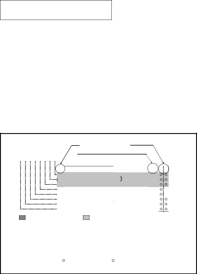
DESCRIPTION FEATURES APPLICATIONS
PIN CONFIGURATION FUNCTIONAL BLOCK PIN DESCRIPTION PART NUMBERING GROUP EXPANSION FUNCTIONAL DESCRIPTION NOTES ON PROGRAMMING DATA REQUIRED FOR MASK ORDERS
ROM PROGRAMMING METHOD FUNCTIONAL DESCRIPTION SUPPLEMENT

HARDWARE
DESCRIPTION/FEATURES/APPLICATIONS/PIN CONFIGURATION
DESCRIPTION
The 3802 group is the 8-bit microcomputer based on the 740 family core technology.
The 3802 group is designed for controlling systems that require analog signal processing and include two serial I/O functions, A-D converters, and D-A converters.
The various microcomputers in the 3802 group include variations of internal memory size and packaging. For details, refer to the section on part numbering.
For details on availability of microcomputers in the 3802 group, refer to the section on group expansion.
FEATURES |
|
•Basic machine-language instructions ....................................... |
71 |
•The minimum instruction execution time ............................ |
0.5 μs |
(at 8 MHz oscillation frequency) |
|
•Memory size |
|
ROM .................................................................. |
8 K to 32 K bytes |
RAM ................................................................. |
384 to 1024 bytes |
•Programmable input/output ports |
............................................. 56 |
|
•Interrupts .................................................. |
|
16 sources, 16 vectors |
•Timers ............................................................................. |
|
8 bit 4 |
•Serial I/O1 .................... |
8-bit 1 (UART or Clock-synchronized) |
|
•Serial I/O2 .................................... |
|
8-bit 1 (Clock-synchronized) |
•PWM ................................................................................ |
|
8-bit 1 |
•A-D converter .................................................. |
|
8-bit 8 channels |
•D-A converter .................................................. |
|
8-bit 2 channels |
•Clock generating circuit ....................... |
|
Internal feedback resistor |
(connect to external ceramic resonator or quartz-crystal oscillator)
•Power source voltage .................................................. |
3.0 to 5.5 V |
(Extended operating temperature version : 4.0 to 5.5 V) |
|
•Power dissipation ............................................................... |
32 mW |
•Memory expansion possible |
–20 to 85°C |
•Operating temperature range .................................... |
|
(Extended operating temperature version : –40 to 85°C)
APPLICATIONS
Office automation, VCRs, tuners, musical instruments, cameras, air conditioners, etc.
PIN CONFIGURATION (TOP VIEW)
P37/RD 

P36/WR 

P35/SYNC 

P34/φ 

P33/RESETOUT 

P32/ONW 

P31/DA2
P30/DA1
VCC
VREF
AVSS
P67/AN7 

P66/AN6 

P65/AN5 

P64/AN4 

P63 /AN3 

P00/AD0 |
P01/AD1 |
P02/AD2 |
P03/AD3 |
P04/AD4 |
P05/AD5 |
P06/AD6 |
|
P07/AD7 |
P10/AD8 |
P11/AD9 |
P12/AD10 |
|
P13/AD11 |
P14/AD12 |
P15/AD13 |
P16/AD14 |
P17/AD15 |
|
|
|
|
|
||||||||||||||||
|
|
|
|
|
|
|
|
|
|
|
|
|
|
|
|
|
|
|
|
|
|
|
|
|
|
|
|
|
|
|
|
|
|
|
|
|
|
|
|
|
|
|
|
|
|
|
|
|
|
|
|
|
|
|
|
|
|
|
|
|
|
|
|
|
|
|
|
|
|
|
|
|
|
|
|
|
|
48 |
47 |
46 |
45 |
44 |
43 |
42 |
41 |
40 |
39 |
38 |
37 |
36 |
35 |
34 |
33 |
|
|
|
|
|
||||||||||||||||||
49 |
|
|
|
|
|
|
|
|
|
|
|
|
|
|
|
|
|
|
|
|
|
|
|
|
|
|
|
|
|
|
|
32 |
|
|
|
|
P20/DB0 |
|
|
|
|
|
|
|
|
|
|
|
|
|
|
|
|
|
|
|
|
|
|
|
|
|
|
|
|
|
|
|
|
|
|
|
|||||
50 |
|
|
|
|
|
|
|
|
|
|
|
|
|
|
|
|
|
|
|
|
|
|
|
|
|
|
|
|
|
|
|
31 |
|
|
|
|
P21/DB1 |
|
|
|
|
|
|
|
|
|
|
|
|
|
|
|
|
|
|
|
|
|
|
|
|
|
|
|
|
|
|
|
|
|
|
|
|
||||
51 |
|
|
|
|
|
|
|
|
|
|
|
|
|
|
|
|
|
|
|
|
|
|
|
|
|
|
|
|
|
|
|
30 |
|
|
|
|
P22/DB2 |
|
|
|
|
|
|
|
|
|
|
|
|
|
|
|
|
|
|
|
|
|
|
|
|
|
|
|
|
|
|
|
|
|
|
|
|
||||
52 |
|
|
|
|
|
|
|
|
|
|
|
|
|
|
|
|
|
|
|
|
|
|
|
|
|
|
|
|
|
|
|
29 |
|
|
|
|
P23/DB3 |
|
|
|
|
|
|
|
|
|
|
|
|
|
|
|
|
|
|
|
|
|
|
|
|
|
|
|
|
|
|
|
|
|
|
|
|
||||
53 |
|
|
|
|
|
|
|
|
|
|
|
|
|
|
|
|
|
|
|
|
|
|
|
|
|
|
|
|
|
|
|
28 |
|
|
|
|
P24/DB4 |
|
54 |
|
|
|
|
|
|
|
|
|
|
|
|
|
|
|
|
|
|
|
|
|
|
|
|
|
|
|
|
|
|
|
27 |
|
|
|
|
P25/DB5 |
|
|
|
|
|
|
|
|
|
|
|
|
|
|
|
|
|
|
|
|
|
|
|
|
|
|
|
|
|
|
|
|
|
|
|
|
||||
55 |
|
|
|
|
|
|
|
|
|
|
|
|
|
|
|
|
|
|
|
|
|
|
|
|
|
|
|
|
|
|
|
26 |
|
|
|
|
P26/DB6 |
|
|
|
|
|
|
|
|
|
|
|
|
|
|
|
|
|
|
|
|
|
|
|
|
|
|
|
|
|
|
|
|
|
|
|
|
||||
56 |
|
|
|
|
|
M38022M4-XXXFP |
|
|
|
|
25 |
|
|
|
|
P27/DB7 |
||||||||||||||||||||||
|
|
|
|
|
|
|
|
|
|
|
|
|
||||||||||||||||||||||||||
57 |
|
|
|
|
|
|
|
|
|
24 |
|
|
|
|
VSS |
|||||||||||||||||||||||
58 |
|
|
|
|
|
|
|
|
|
|
|
|
|
|
|
|
|
|
|
|
|
|
|
|
|
|
|
|
|
|
|
23 |
|
|
|
|
XOUT |
|
59 |
|
|
|
|
|
|
|
|
|
|
|
|
|
|
|
|
|
|
|
|
|
|
|
|
|
|
|
|
|
|
|
22 |
|
|
|
|
XIN |
|
|
|
|
|
|
|
|
|
|
|
|
|
|
|
|
|
|
|
|
|
|
|
|
|
|
|
|
|
|
|
|
|
|
|
|
||||
60 |
|
|
|
|
|
|
|
|
|
|
|
|
|
|
|
|
|
|
|
|
|
|
|
|
|
|
|
|
|
|
|
21 |
|
|
|
|
P40/INT4 |
|
|
|
|
|
|
|
|
|
|
|
|
|
|
|
|
|
|
|
|
|
|
|
|
|
|
|
|
|
|
|
|
|
|
|
|
||||
61 |
|
|
|
|
|
|
|
|
|
|
|
|
|
|
|
|
|
|
|
|
|
|
|
|
|
|
|
|
|
|
|
20 |
|
|
|
|
P41/INT0 |
|
|
|
|
|
|
|
|
|
|
|
|
|
|
|
|
|
|
|
|
|
|
|
|
|
|
|
|
|
|
|
|
|
|
|
|||||
62 |
|
|
|
|
|
|
|
|
|
|
|
|
|
|
|
|
|
|
|
|
|
|
|
|
|
|
|
|
|
|
|
19 |
|
|
|
|
RESET |
|
|
|
|
|
|
|
|
|
|
|
|
|
|
|
|
|
|
|
|
|
|
|
|
|
|
|
|
|
|
|
|
|
|
|
|
||||
63 |
|
|
|
|
|
|
|
|
|
|
|
|
|
|
|
|
|
|
|
|
|
|
|
|
|
|
|
|
|
|
|
18 |
|
|
|
|
CNVSS |
|
|
|
|
|
|
|
|
|
|
|
|
|
|
|
|
|
|
|
|
|
|
|
|
|
|
|
|
|
|
|
|
|
|
|
|
||||
64 |
|
|
|
|
|
|
|
|
|
|
|
|
|
|
|
|
|
|
10 |
11 |
12 |
13 |
|
|
15 |
17 |
|
|
|
|
P42/INT1 |
|||||||
|
|
|
|
|
|
|
|
|
|
|
|
|
|
|
|
|
|
|
|
|
|
|
|
|||||||||||||||
1 |
2 |
3 |
4 |
5 |
6 |
7 |
8 |
9 |
14 |
16 |
|
|
|
|
|
|||||||||||||||||||||||
|
|
|
|
|
|
|
|
|
|
|
|
|
|
|
|
|
|
|
|
|
|
|
|
|
|
|
|
|
|
|
|
|
|
|
|
|
|
|
|
|
|
|
|
|
|
|
|
|
|
|
|
|
|
|
|
|
|
|
|
|
|
|
|
|
|
|
|
|
|
|
|
|
|
|
|
|
|
P62/AN2 |
P61/AN1 |
P60/AN0 |
P57/INT3 |
P56/PWM |
P55/CNTR1 |
P54/CNTR0 |
|
P53/SRDY2 |
P52/SCLK2 |
P51/SOUT2 |
P50/SIN2 |
|
P47/SRDY1 |
P46/SCLK1 |
P45/TXD |
P44/RXD |
P43/INT2 |
|
|
|
|
|
||||||||||||||||
|
|
|
|
|
|
|
||||||||||||||||||||||||||||||||
|
|
|
|
|
|
|
||||||||||||||||||||||||||||||||
Package type : 64P6N-A 64-pin plastic-molded QFP
Fig. 1 Pin configuration of M38022M4-XXXFP
1-2 |
3802 GROUP USER’S MANUAL |
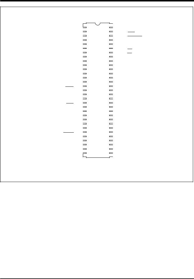
HARDWARE
PIN CONFIGURATION
PIN CONFIGURATION (TOP VIEW)
VCC 1
VREF 
 2
2
AVSS 
 3
3
P67/AN7 

 4
4
P66/AN6 

 5
5
P65/AN5 

 6
6
P64/AN4 

 7
7
P63/AN3 

 8
8
P62/AN2 

 9
9
P61/AN1 

 10
10
P60/AN0 

 11
11
P57/INT3 

 12
12
P56/PWM 

 13
13
P55/CNTR1 

 14
14
P54/CNTR0 

 15
15
P53/SRDY2 

 16
16
P52/SCLK2 

 17
17
P51/SOUT2 

 18
18
P50/SIN2 

 19
19
P47/SRDY1 

 20
20
P46/SCLK1 

 21
21
P45/TXD 

 22 P44/RXD

 23 P43/INT2

 24 P42/INT1

 25
25
CNVSS 
 26
26
RESET 
 27 P41/INT0

 28 P40/INT4

 29
29
XIN 
 30 XOUT
 31
31
VSS 32
XXXSP-M38022M4
64


63


62


61


60


59


58


57


56


55


54


53


52


51


50


49


48


47


46


45


44


43


42


41


40


39


38


37


36


35


34


33


P3
P3
P3
P3
P3
P3 P3 P3 P0 P0 P0 P0 P0 P0 P0 P0 P1 P1 P1 P1 P1 P1 P1 P1 P2 P2 P2 P2 P2 P2 P2 P2
0/DA1
1/DA2
2/ONW
3/RESETOUT
4/φ
5/SYNC
6/WR
7/RD
0/AD0
1/AD1
2/AD2
3/AD3
4/AD4
5/AD5
6/AD6
7/AD7
0/AD8
1/AD9
2/AD10
3/AD11
4/AD12
5/AD13
6/AD14
7/AD15
0/DB0
1/DB1
2/DB2
3/DB3
4/DB4
5/DB5
6/DB6
7/DB7
Package type : 64P4B 64-pin shrink plastic-molded DIP
Fig.2 Pin configuration of M38022M4-XXXSP
3802 GROUP USER'S MANUAL |
1-3 |

4-1
MANUAL USER’S GROUP 3802
diagram block Functional 3 .Fig
FUNCTIONAL BLOCK DIAGRAM (Package : 64P4B)
Clock input |
Clock output |
|
|
Reset input |
|
|
VSS |
VCC |
RESET |
CNVSS |
|||
XIN |
XOUT |
|||||
30 |
31 |
32 |
1 |
27 |
26 |
Clock generating circuit
|
Timer 1 (8) |
Prescaler 12 (8) |
Timer 2 (8) |
Prescaler X (8) |
Timer X (8) |
Prescaler Y (8) |
Timer Y (8) |
A-D |
|
|
D-A |
D-A |
converter |
PWM (8) |
SI/O2 (8) SI/O1 (8) |
converter 2 |
converter 1 |
(8) |
(8) |
(8) |
INT0
|
|
|
~ |
|
|
|
|
INT3 |
|
INT2 |
|
|
|
|
|
|
INT4 |
|
|
|
P6(8) |
P5(8) |
P4(8) |
P3(8) |
P2(8) |
P1(8) |
P0(8) |
2 |
3 |
4 |
5 |
6 |
7 |
8 |
9 10 11 |
12 13 14 15 16 17 18 19 |
20 21 22 23 24 25 28 29 |
57 58 59 60 61 62 63 64 |
33 34 35 36 37 38 39 40 |
41 42 43 44 45 46 47 48 |
49 50 51 52 53 54 55 56 |
VREF AVSS
I/O port P6 |
I/O port P5 |
I/O port P4 |
I/O port P3 |
I/O port P2 |
I/O port P1 |
I/O port P0 |
BLOCK FUNCTIONAL |
|
BLOCK FUNCTIONAL |
HARDWARE |
|
|
|
|

|
|
|
|
|
|
|
|
|
|
|
HARDWARE |
|
|
|
|
|
|
|
|
|
|
|
PIN DESCRIPTION |
|
|
|
|
|
|
|
|
|
|
|
|
PIN DESCRIPTION |
|
|
|
|
|
||||||
Table 1. Pin description |
|
|
|
|
|
||||||
|
|
|
|
|
|
|
|
|
|
|
|
|
|
Pin |
Name |
Function |
|
|
|
|
|||
|
|
|
Function except a port function |
||||||||
|
|
|
|
|
|
|
|
|
|
|
|
|
|
|
|
|
|
|
|
|
|
|
|
|
VCC, VSS |
Power source |
• Apply voltage of 3.0 V–5.5 V to VCC, and 0 V to VSS. |
|
|||||||
|
|
|
|
|
|
|
(Extended operating temperature version : 4.0 V to 5.5 V) |
|
|||
|
|
|
|
|
|
|
|
|
|
|
|
|
CNVSS |
CNVSS |
• This pin controls the operation mode of the chip. |
|
|||||||
|
|
|
|
|
|
|
• Normally connected to VSS. |
|
|||
|
|
|
|
|
|
|
• If this pin is connected to VCC, the internal ROM is inhibited and external memory is accessed. |
||||
|
|
|
|
|
|
|
|
|
|
|
|
|
VREF |
Analog reference |
• Reference voltage input pin for A-D and D-A converters |
|
|||||||
|
|
|
|
|
|
voltage |
|
|
|
|
|
|
|
|
|
|
|
|
|
|
|
|
|
|
AVSS |
Analog power |
• GND input pin for A-D and D-A converters |
|
|||||||
|
|
|
|
|
|
source |
• Connect to VSS. |
|
|||
|
|
|
|
|
|
|
|
|
|
|
|
|
|
|
|
|
|
|
|
|
|||
|
RESET |
Reset input |
• Reset input pin for active “L” |
|
|||||||
|
|
|
|
|
|
|
|
|
|
|
|
|
XIN |
Clock input |
• Input and output signals for the clock generating circuit. |
|
|||||||
|
|
|
|
|
|
|
• Connect a ceramic resonator or quartz-crystal oscillator between the XIN and XOUT pins to set the |
||||
|
|
|
|
|
|
|
|||||
|
XOUT |
Clock output |
oscillation frequency. |
|
|||||||
|
|
|
|
|
|
|
• If an external clock is used, connect the clock source to the XIN pin and leave the XOUT pin open. |
||||
|
|
|
|
|
|
|
• The clock is used as the oscillating source of system clock. |
||||
|
|
|
|
|
|
|
|
|
|
|
|
|
P00–P07 |
I/O port P0 |
• 8 bit CMOS I/O port |
|
|||||||
|
|
|
|
|
|
|
• I/O direction register allows each pin to be individually programmed as either input or output. |
||||
|
|
|
|
|
|
|
|||||
|
P10–P17 |
I/O port P1 |
• At reset this port is set to input mode. |
|
|||||||
|
|
|
|
|
|
|
• In modes other than single-chip, these pins are used as address, data, and control bus I/O pins. |
||||
|
|
|
|
|
|
|
|||||
|
P20–P27 |
I/O port P2 |
• CMOS compatible input level |
|
|||||||
|
|
|
|
|
|
|
• CMOS 3-state output structure |
|
|
||
|
P30/DA1, |
I/O port P3 |
|
• D–A conversion output pins |
|||||||
|
|
|
|
|
|||||||
|
P31/DA2 |
|
|
|
|
|
|
||||
|
|
|
|
|
|
|
|
|
|
|
|
|
P32–P37 |
|
|
|
|
|
|
||||
|
|
|
|
|
|
|
|
|
|
|
|
|
P40/INT4, |
I/O port P4 |
• 8-bit CMOS I/O port with the same function as port P0 |
|
|
• External interrupt input pin |
|||||
|
P41/INT0, |
|
• CMOS compatible input level |
|
|
|
|||||
|
P42/INT1, |
|
• CMOS 3-state output structure |
|
|
|
|||||
|
P43/INT2 |
|
|
|
|
|
|
||||
|
|
|
|
|
|
|
|
|
|
|
|
|
P44/RXD, |
|
|
|
|
|
• Serial I/O1 I/O pins |
||||
|
P45/TXD, |
|
|
|
|
|
|
||||
|
P46/SCLK1, |
|
|
|
|
|
|
||||
|
|
|
|
|
|
|
|
|
|
|
|
|
P47/SRDY1 |
|
|
|
|
|
|
||||
|
|
|
|
|
|
|
|
|
|
|
|
|
P50/SIN2, |
I/O port P5 |
• 8-bit CMOS I/O port with the same function as port P0 |
|
|
• Serial I/O2 I/O pins |
|||||
|
P51/SOUT2, |
|
• CMOS compatible input level |
|
|
|
|||||
|
P52/SCLK2, |
|
• CMOS 3-state output structure |
|
|
|
|||||
|
|
|
|
|
|
|
|
|
|
||
|
P53/SRDY2 |
|
|
|
|
|
|
||||
|
|
|
|
|
|
|
|
|
|
|
|
|
P54/CNTR0, |
|
|
|
|
|
• Timer X and Timer Y I/O pins |
||||
|
P55/CNTR1 |
|
|
|
|
|
|
||||
|
|
|
|
|
|
|
|
|
|
|
|
|
P56/PWM |
|
|
|
|
|
• PWM output pin |
||||
|
|
|
|
|
|
|
|
|
|
|
|
|
P57/INT3 |
|
|
|
|
|
• External interrupt input pin |
||||
|
|
|
|
|
|
|
|||||
|
P60/AN0– |
I/O port P6 |
• 8-bit CMOS I/O port with the same function as port P0 |
|
|
• A-D conversion input pins |
|||||
|
P67/AN7 |
|
• CMOS compatible input level |
|
|
|
|||||
|
|
|
|
|
|
|
• CMOS 3-state output structure |
|
|
|
|
|
|
|
|
|
|
|
|
|
|
|
|
3802 GROUP USER'S MANUAL |
1-5 |
HARDWARE
PART NUMBERING
PART NUMBERING
Product M3802 2 M 4 - XXX SP
 Package type
SP : 64P4B package
FP : 64P6N-A package
SS : 64S1B-E package
FS : 64D0 package
ROM number
Omitted in some types.
Normally, using hyphen.
When electrical characteristic, or division of quality identification code using alphanumeric character
– : standard
D : Extended operating temperature version
ROM/PROM size 1 : 4096 bytes 2 : 8192 bytes
3 : 12288 bytes
4 : 16384 bytes
5 : 20480 bytes
6 : 24576 bytes
7 : 28672 bytes
8 : 32768 bytes
The first 128 bytes and the last 2 bytes of ROM are reserved areas ; they cannot be used.
Memory type
M : Mask ROM version
E : EPROM or One Time PROM version
RAM size
0 : 192 bytes
1 : 256 bytes
2 : 384 bytes
3 : 512 bytes
4 : 640 bytes
5 : 768 bytes
6 : 896 bytes
7 : 1024 bytes
Fig.4 Part numbering
1-6 |
3802 GROUP USER’S MANUAL |
HARDWARE
GROUP EXPANSION
GROUP EXPANSION
Mitsubishi plans to expand the 3802 group as follows:
(1) Support for mask ROM, One Time PROM, and EPROM
versions |
|
ROM/PROM capacity ................................... |
8 K to 32 K bytes |
RAM capacity .............................................. |
384 to 1024 bytes |
(2) Packages |
|
64P4B ............................................ |
Shrink plastic molded DIP |
64P6N-A ................................................... |
Plastic molded QFP |
64S1B-E .................................................... |
Shrink ceramic DIP |
64D0 ................................................................... |
Ceramic LCC |
Memory Expansion Plan |
|
|
|
|
|
|
|
|
|
|
|
|
|
|
|
|
|||||
|
|
|
|
|
|
|
|
|
|
|
|
|
|
|
|
|
|||||
ROM size (bytes) |
|
|
|
|
|
|
|
|
|
|
|
|
Mass product |
|
|
||||||
32K |
|
|
|
|
|
|
|
|
|
|
|
|
|
|
|
|
|
|
M38027M8/E8 |
|
|
|
|
|
|
|
|
|
|
|
|
|
|
|
|
|
|
|
|
||||
28K |
|
|
|
|
|
|
|
|
|
|
|
|
|
|
|
|
|
|
|
|
|
|
|
|
|
|
|
|
|
|
|
|
|
|
|
|
|
|
|
|
|
|
|
|
|
|
|
|
|
|
|
|
|
|
Mass product |
|
|
|
|
|
|
|
|
|
|
24K |
|
|
|
|
|
|
|
|
|
|
|
M38024M6 |
|
|
|
|
|
|
|
||
20K |
|
|
|
|
|
|
|
|
|
|
|
|
|
|
|
|
|
|
|
|
|
|
|
|
|
|
|
|
|
|
|
|
|
|
|
|
|
|
|
|
|
|
|
|
|
|
|
Mass product |
|
|
|
|
|
|
|
|
|
|
|
|
|
|
|
||
16K |
|
|
|
|
|
|
M38022M4 |
|
|
|
|
|
|
|
|
|
|||||
12K |
|
|
|
|
|
|
|
|
|
|
|
|
|
|
|
|
|
|
|
|
|
|
|
|
|
|
|
|
|
|
|
|
|
|
|
|
|
|
|
|
|
|
|
|
|
|
|
Mass product |
|
|
|
|
|
|
|
|
|
|
|
|
|
|
|
||
8K |
|
|
|
|
|
|
M38022M2 |
|
|
|
|
|
|
|
|
|
|||||
4K |
|
|
|
|
|
|
|
|
|
|
|
|
|
|
|
|
|
|
|
|
|
|
|
|
|
|
|
|
|
|
|
|
|
|
|
|
|
|
|
|
|
||
|
|
|
|
|
|
|
|
|
|
|
|
|
|
|
|
|
|
|
|
|
|
|
|
|
192 |
256 |
|
|
384 |
512 |
|
640 |
768 |
896 |
1024 |
|
|||||||
|
|
|
|
|
|
|
|
|
|
RAM size (bytes) |
|
|
|
|
|
|
|
|
|
||
|
|
|
|
|
|
|
|
|
|
|
|
|
|
|
|
|
|
|
|
|
|
Fig. 5 Memory expansion plan |
|
|
|
|
|
|
|
|
|
|
|
|
|
|
|
|
|||||
Currently supported products are listed below |
|
|
|
|
|
|
|
|
|
|
|
|
|
||||||||
Table 2. List of supported products |
|
|
|
|
|
|
|
|
|
|
|
|
|
|
|
As of May 1996 |
|||||
Product |
(P) ROM size (bytes) |
|
RAM size (bytes) |
|
Package |
|
|
|
|
Remarks |
|||||||||||
ROM size for User in ( |
) |
|
|
|
|
|
|
||||||||||||||
|
|
|
|
|
|
|
|
|
|
|
|
|
|
|
|
|
|||||
|
|
|
|
|
|
|
|
|
|
|
|
|
|
|
|
|
|
|
|
||
M38022M2-XXXSP |
8192 |
|
|
|
|
384 |
|
|
64P4B |
|
|
Mask ROM version |
|||||||||
M38022M2-XXXFP |
(8062) |
|
|
|
|
|
|
64P6N-A |
|
Mask ROM version |
|||||||||||
|
|
|
|
|
|
|
|
|
|||||||||||||
M38022M4-XXXSP |
16384 |
|
|
|
|
384 |
|
|
64P4B |
|
|
Mask ROM version |
|||||||||
M38022M4-XXXFP |
(16254) |
|
|
|
|
|
|
64P6N-A |
|
Mask ROM version |
|||||||||||
|
|
|
|
|
|
|
|
|
|||||||||||||
|
|
|
|
|
|
|
|
|
|
|
|
||||||||||
|
|
|
|
|
|
|
|
|
|
|
|
|
|
|
|
|
|
|
|
||
M38024M6-XXXSP |
24576 |
|
|
|
|
640 |
|
|
64P4B |
|
|
Mask ROM version |
|||||||||
M38024M6-XXXFP |
(24446) |
|
|
|
|
|
|
64P6N-A |
|
Mask ROM version |
|||||||||||
|
|
|
|
|
|
|
|
|
|||||||||||||
|
|
|
|
|
|
|
|
|
|
|
|
|
|
|
|
|
|
|
|
||
M38027M8-XXXSP |
|
|
|
|
|
|
|
|
|
|
|
|
|
|
Mask ROM version |
||||||
|
|
|
|
|
|
|
|
|
|
|
|
|
|
|
|
|
|
|
|
||
M38027E8-XXXSP |
|
|
|
|
|
|
|
|
|
|
|
64P4B |
|
|
One Time PROM version |
||||||
M38027E8SP |
|
|
|
|
|
|
|
|
|
|
|
|
|
|
One Time PROM version (blank) |
||||||
|
|
|
|
|
|
|
|
|
|
|
|
|
|
|
|
|
|
|
|
||
M38027M8-XXXFP |
32768 |
|
|
|
|
1024 |
|
|
|
|
|
Mask ROM version |
|||||||||
M38027E8-XXXFP |
(32638) |
|
|
|
|
|
|
64P6N-A |
|
One Time PROM version |
|||||||||||
|
|
|
|
|
|
|
|
|
|||||||||||||
M38027E8FP |
|
|
|
|
|
|
|
|
|
|
|
|
|
|
One Time PROM version (blank) |
||||||
|
|
|
|
|
|
|
|
|
|
|
|
|
|
|
|
|
|
|
|||
M38027E8SS |
|
|
|
|
|
|
|
|
|
|
|
64S1B-E |
|
EPROM version |
|||||||
|
|
|
|
|
|
|
|
|
|
|
|
|
|
|
|
|
|
|
|
||
M38027E8FS |
|
|
|
|
|
|
|
|
|
|
|
64D0 |
|
|
EPROM version |
||||||
3802 GROUP USER'S MANUAL |
1-7 |

HARDWARE
GROUP EXPANSION
GROUP EXPANSION
(Extended operating temperature version)
Mitsubishi plans to expand the 3802 group (extended operating temperature version) as follows:
(1)Support for mask ROM One Time PROM, and EPROM versions
ROM/PROM capacity ................................... |
8 K to 32 K bytes |
RAM capacity .............................................. |
384 to 1024 bytes |
(2) Packages |
|
64P4B ............................................ |
Shrink plastic molded DIP |
64P6N-A ................................................... |
Plastic molded QFP |
Memory Expansion Plan (Extended operating temperature version)
ROM size (bytes) |
|
|
|
|
|
Mass product |
|
32K |
|
|
|
|
|
|
M38027M8D/E8D |
28K |
|
|
|
|
|
|
|
24K |
|
|
|
|
|
|
|
20K |
|
|
|
|
|
|
|
Mass product |
|
|
|
|
|
||
16K |
|
M38022M4D |
|
|
|
|
|
12K |
|
|
|
|
|
|
|
Mass product |
|
|
|
|
|
||
8K |
|
M38022M2D |
|
|
|
|
|
4K |
|
|
|
|
|
|
|
192 |
256 |
384 |
512 |
640 |
768 |
896 |
1024 |
|
|
RAM size (bytes) |
|
|
|
|
|
Fig. 6 Memory expansion plan (Extended operating temperature version)
Currently supported products are listed below. |
|
|
|
||
Table 3. List of supported products (Extended operating temperature version) |
As of May 1996 |
||||
Product |
(P) ROM size (bytes) |
RAM size (bytes) |
Package |
|
Remarks |
M38022M2DXXXSP |
8192 |
384 |
64P4B |
|
Mask ROM version |
M38022M2DXXXFP |
(8062) |
64P6N-A |
|
Mask ROM version |
|
|
|
||||
M38022M4DXXXSP |
16384 |
384 |
64P4B |
|
Mask ROM version |
M38022M4DXXXFP |
(16254) |
64P6N-A |
|
Mask ROM version |
|
|
|
||||
M38027M8DXXXSP |
|
|
|
|
Mask ROM version |
M38027E8DXXXSP |
|
|
64P4B |
|
One Time PROM version |
M38027E8DSP |
32768 |
1024 |
|
|
One Time PROM version (blank) |
M38027M8DXXXFP |
(32638) |
|
|
Mask ROM version |
|
|
|
|
|||
M38027E8DXXXFP |
|
|
64P6N-A |
|
One Time PROM version |
M38027E8DFP |
|
|
|
|
One Time PROM version (blank) |
1-8 |
3802 GROUP USER’S MANUAL |

HARDWARE
FUNCTIONAL DESCRIPTION
FUNCTIONAL DESCRIPTION
Central Processing Unit (CPU)
The 3802 group uses the standard 740 family instruction set. Refer to the table of 740 family addressing modes and machine instructions or the SERIES 740 <Software> User´s Manual for details on the instruction set.
Machine-resident 740 family instructions are as follows:
The FST and SLW instructions cannot be used.
The MUL, DIV, WIT and STP instruction can be used. The central processing unit (CPU) has the six registers.
Accumulator (A)
The accumulator is an 8-bit register. Data operations such as data transfer, etc., are executed mainly through the accumulator.
Index register X (X), Index register Y (Y)
Both index register X and index register Y are 8-bit registers. In the index addressing modes, the value of the OPERAND is added to the contents of register X or register Y and specifies the real address.
When the T flag in the processor status register is set to “1”, the value contained in index register X becomes the address for the second OPERAND.
Stack pointer (S)
The stack pointer is an 8-bit register used during sub-routine calls and interrupts. The stack is used to store the current address data and processor status when branching to subroutines or interrupt routines.
The lower eight bits of the stack address are determined by the contents of the stack pointer. The upper eight bits of the stack address are determined by the Stack Page Selection Bit. If the Stack Page Selection Bit is “0”, then the RAM in the zero page is used as the stack area. If the Stack Page Selection Bit is “1”, then RAM in page 1 is used as the stack area.
The Stack Page Selection Bit is located in the SFR area in the zero page. Note that the initial value of the Stack Page Selection Bit varies with each microcomputer type. Also some microcomputer types have no Stack Page Selection Bit and the upper eight bits of the stack address are fixed. The operations of pushing register contents onto the stack and popping them from the stack are shown in Fig.7.
Program counter (PC)
The program counter is a 16-bit counter consisting of two 8-bit registers
PCH and PCL. It is used to indicate the address of the next instruction to
be executed.
|
b7 |
b0 |
||
|
A |
|
|
Accumulator |
|
b7 |
b0 |
||
|
|
|
|
Index Register X |
|
X |
|
|
|
|
b7 |
b0 |
||
|
|
|
|
Index Register Y |
|
Y |
|
|
|
|
b7 |
b0 |
||
|
|
|
|
Stack Pointer |
|
S |
|
|
|
b15 |
b7 |
b0 |
||
|
|
|
|
Program Counter |
PCH |
PCL |
|
|
|
|
b7 |
b0 |
||
N V T B D I Z C Processor Status Register (PS)
Carry Flag
Zero Flag
Interrupt Disable Flag
Decimal Mode Flag
Break Flag
Index X Mode Flag
Overflow Flag
Negative Flag
Fig. 7. 740 Family CPU register structure
3802 GROUP USER’S MANUAL |
1-9 |
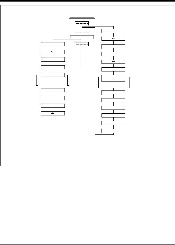
HARDWARE
FUNCTIONAL DESCRIPTION

 On-going Routine

Interrupt request  (Note 1)
Execute JSR
M (S) (PCH)
(PCH)
(S) (S – 1)
Store Return Address
on Stack (Note 2)
M (S) (PCL)
(PCL)
(S) (S – 1)
Subroutine
Execute RTS
Restore Return
Address
(S) (S + 1)
(PCL) M (S)
M (S)
(S) (S + 1)
(PCH) M (S)
M (S) (PCH)
(PCH)
(S) (S – 1)
Store Return Address
on Stack (Note 2)
M (S) (PCL)
(PCL)
(S)  (S – 1)
M (S) (PS)
(S)  (S – 1)
Interrupt
Service Routine
Execute RTI
(S)  (S + 1)
(PS) M (S)
M (S)
(S)  (S + 1)
(PCL) M (S)
M (S)
(S)  (S + 1)
(PCH) M (S)
M (S)
Store Contents of Processor Status Register on Stack
I Flag “0” to “1” Fetch the Jump Vector
Restore Contents of
Processor Status Register
Restore Return
Address
Note 1 : The condition to enable the interrupt  Interrupt enable bit is “1”
Interrupt disable flag is “0”
2 : When an interrupt occurs, the address of the next instruction to be executed is stored in the stack area. When a subroutine is called, the address one before the next instruction to be executed is stored in the stack area.
Fig. 8. Register push and pop at interrupt generation and subroutine call
Table. 4. Push and pop instructions of accumulator or processor status register
|
Push instruction to stack |
Pop instruction from stack |
|
|
|
Accumulator |
PHA |
PLA |
|
|
|
Processor status register |
PHP |
PLP |
|
|
|
1-10 |
3802 GROUP USER’S MANUAL |

HARDWARE
FUNCTIONAL DESCRIPTION
Processor status register (PS)
The processor status register is an 8-bit register consisting of flags which indicate the status of the processor after an arithmetic operation. Branch operations can be performed by testing the Carry (C) flag, Zero (Z) flag, Overflow (V) flag, or the Negative (N) flag. In decimal mode, the Z, V, N flags are not valid.
After reset, the Interrupt disable (I) flag is set to “1”, but all other flags are undefined. Since the Index X mode (T) and Decimal mode (D) flags directly affect arithmetic operations, they should be initialized in the beginning of a program.
(1)Carry flag (C)
The C flag contains a carry or borrow generated by the arithmetic logic unit (ALU) immediately after an arithmetic operation. It can also be changed by a shift or rotate instruction.
(2)Zero flag (Z)
The Z flag is set if the result of an immediate arithmetic operation or a data transfer is “0”, and cleared if the result is anything other than “0”.
(3)Interrupt disable flag (I)
The I flag disables all interrupts except for the interrupt generated by the BRK instruction.
Interrupts are disabled when the I flag is “1”.
When an interrupt occurs, this flag is automatically set to “1” to prevent other interrupts from interfering until the current interrupt is serviced.
(4)Decimal mode flag (D)
The D flag determines whether additions and subtractions are executed in binary or decimal. Binary arithmetic is executed when this flag is “0”; decimal arithmetic is executed when it is “1”. Decimal correction is automatic in decimal mode. Only the ADC and SBC instructions can be used for decimal arithmetic.
(5)Break flag (B)
The B flag is used to indicate that the current interrupt was generated by the BRK instruction. The BRK flag in the processor status register is always “0”. When the BRK instruction is used to generate an interrupt, the processor status register is pushed onto the stack with the break flag set to “1”. The saved processor status is the only place where the break flag is ever set.
(6)Index X mode flag (T)
When the T flag is “0”, arithmetic operations are performed between accumulator and memory, e.g. the results of an operation between two memory locations is stored in the accumulator. When the T flag is “1”, direct arithmetic operations and direct data transfers are enabled between memory locations, i.e. between memory and memory, memory and I/O, and I/O and I/O. In this case, the result of an arithmetic operation performed on data in memory location 1 and memory location 2 is stored in memory location 1. The address of memory location 1 is specified by index register X, and the address of memory location 2 is specified by normal addressing modes.
(7)Overflow flag (V)
The V flag is used during the addition or subtraction of one byte of signed data. It is set if the result exceeds +127 to -128. When the BIT instruction is executed, bit 6 of the memory location operated on by the BIT instruction is stored in the overflow flag.
(8)Negative flag (N)
The N flag is set if the result of an arithmetic operation or data transfer is negative. When the BIT instruction is executed, bit 7 of the memory location operated on by the BIT instruction is stored in the negative flag.
Table. 5. Set and clear instructions of each bit of processor status register
|
C flag |
Z flag |
I flag |
D flag |
B flag |
T flag |
V flag |
N flag |
|
|
|
|
|
|
|
|
|
Set instruction |
SEC |
_ |
SEI |
SED |
_ |
SET |
_ |
_ |
|
|
|
|
|||||
Clear instruction |
CLC |
_ |
CLI |
CLD |
_ |
CLT |
CLV |
_ |
|
|
|
3802 GROUP USER’S MANUAL |
1-11 |

HARDWARE
FUNCTIONAL DESCRIPTION
CPU Mode Register
The CPU mode register is allocated at address 003B16. The CPU mode
register contains the stack page selection bit.
|
b7 |
|
|
|
|
|
|
b0 |
|
|
||||||||||
|
|
|
|
|
|
|
|
|
|
|
|
|
|
|
|
|
CPU mode register |
|||
|
|
|
|
|
|
|
|
|
|
|
|
|
|
|
|
|
(CPUM : address 003B16) |
|||
|
|
|
|
|
|
|
|
|
|
|
|
|
|
|
|
|
||||
|
|
|
|
|
|
|
|
|
|
|
|
|
|
|
|
|
|
Processor mode bits |
||
|
|
|
|
|
|
|
|
|
|
|
|
|
|
|
|
|
|
|||
|
|
|
|
|
|
|
|
|
|
|
|
|
|
|
|
|
|
b1 |
b0 |
|
|
|
|
|
|
|
|
|
|
|
|
0 |
0 |
: Single-chip mode |
|||||||
|
|
|
|
|
|
|
|
|
|
|
0 |
1 |
: Memory expansion mode |
|||||||
|
|
|
|
|
|
|
|
|
|
|
1 |
0 |
: Microprocessor mode |
|||||||
|
|
|
|
|
|
|
|
|
|
|
1 |
1 |
: Not available |
|||||||
|
|
|
|
|
|
|
|
|
|
|
|
|
|
|
|
|
|
Stack page selection bit |
||
|
|
|
|
|
|
|
|
|
|
|
|
|
|
|
|
|
|
|||
|
|
|
|
|
|
|
|
|
|
0 |
: 0 page |
|||||||||
|
|
|
|
|
|
|
|
|
|
1 |
: 1 page |
|||||||||
|
|
|
|
|
|
|
|
|
|
|
|
|
|
|
|
|
|
Not used (return “0” when read) |
||
|
|
|
|
|
|
|
|
|
|
|
|
|
|
|
|
|
|
|||
|
|
|
|
|
|
|
|
|
|
|
|
|
|
|
|
|
|
|
|
|
Fig. 9. Structure of CPU mode register |
|
|
|
|
|
|
|
|
|
|
|
|
||||||||
1-12 |
3802 GROUP USER’S MANUAL |

HARDWARE
FUNCTIONAL DESCRIPTION
Memory
Special function register (SFR) area
The Special Function Register area in the zero page contains control registers such as I/O ports and timers.
RAM
RAM is used for data storage and for stack area of subroutine calls and interrupts.
Zero page
The 256 bytes from addresses 000016 to 00FF16 are called the zero page area. The internal RAM and the special function registers (SFR) are allocated to this area.
The zero page addressing mode can be used to specify memory and register addresses in the zero page area. Access to this area with only 2 bytes is possible in the zero page addressing mode.
ROM
The first 128 bytes and the last 2 bytes of ROM are reserved for device testing and the rest is user area for storing programs.
Interrupt vector area
The interrupt vector area contains reset and interrupt vectors.
Special page
The 256 bytes from addresses FF0016 to FFFF16 are called the special page area. The special page addressing mode can be used to specify memory addresses in the special page area. Access to this area with only 2 bytes is possible in the special page addressing mode.
RAM area
RAM capacity |
Address |
|
000016 |
|
|
|
|
||||
|
|
|
|
|
|||||||
(bytes) |
XXXX16 |
|
SFR area |
|
|
|
|||||
|
|
|
|
|
|
|
|
|
|||
|
|
|
|
|
|
|
|
|
|
|
|
192 |
00FF16 |
|
|
|
|
|
|
|
|
|
Zero page |
256 |
013F16 |
|
|
004016 |
|
|
|
|
|||
|
|
|
|
|
|
|
|
|
|
||
384 |
01BF16 |
|
|
010016 |
|
|
|
|
|||
512 |
023F16 |
|
|
|
|
|
|
||||
|
RAM |
|
|
|
|
|
|
|
|
||
640 |
02BF16 |
|
|
|
|
|
|
|
|
|
|
|
|
|
|
|
|
|
|
|
|
||
768 |
033F16 |
|
|
|
|
|
|
|
|
|
|
896 |
03BF16 |
|
|
|
|
|
XXXX16 |
|
|
|
|
1024 |
043F16 |
|
|
|
|
|
|
|
|
|
|
|
|
|
|
|
|
|
|
Reserved area |
|
|
|
ROM area |
|
|
044016 |
|
|
|
|
||||
|
|
Not used |
|
|
|
||||||
|
|
|
|
|
|
|
|
|
|
||
ROM capacity |
Address |
Address |
|
|
|
|
|
|
|
|
|
(bytes) |
YYYY16 |
ZZZZ16 |
|
|
|
|
YYYY16 |
Reserved ROM area |
|
|
|
4096 |
F00016 |
F08016 |
|
|
|
|
|
|
|
|
|
8192 |
E00016 |
E08016 |
|
|
|
|
|
(128 bytes) |
|
|
|
|
|
|
|
|
|
|
|
|
|||
12288 |
D00016 |
D08016 |
|
|
|
|
ZZZZ16 |
|
|
|
|
|
|
|
|
|
|
|
|
||||
16384 |
C00016 |
C08016 |
|
|
|
|
|
|
|
|
|
20480 |
B00016 |
B08016 |
|
|
|
|
|
|
|
|
|
24576 |
A00016 |
A08016 |
|
|
|
|
|
|
|
|
|
28672 |
900016 |
908016 |
ROM |
|
|
|
|
|
|||
32768 |
800016 |
808016 |
|
|
|
|
|||||
|
|
|
|
FF0016 |
|
|
|
|
|||
|
|
|
|
|
|
|
|
|
|
|
|
|
|
|
|
|
|
|
FFDC16 |
|
|
|
Special page |
|
|
|
Interrupt vector area |
|
|
||||||
|
|
|
|
|
|
|
|
|
|
||
|
|
|
|
|
|
|
|
|
|
|
|
|
|
|
|
|
|
|
FFFE16 |
|
|
|
|
|
|
|
Reserved ROM area |
|
|
|
|||||
|
|
|
|
|
|
|
FFFF16 |
|
|
|
|
Fig. 10 Memory map diagram
3802 GROUP USER’S MANUAL |
1-13 |

HARDWARE
FUNCTIONAL DESCRIPTION
000016 |
Port P0 (P0) |
002016 |
Prescaler 12 (PRE12) |
|
|
|
|
000116 |
Port P0 direction register (P0D) |
002116 |
Timer 1 (T1) |
|
|
|
|
000216 |
Port P1 (P1) |
002216 |
Timer 2 (T2) |
|
|
|
|
000316 |
Port P1 direction register (P1D) |
002316 |
Timer XY mode register (TM) |
|
|
|
|
000416 |
Port P2 (P2) |
002416 |
Prescaler X (PREX) |
|
|
|
|
000516 |
Port P2 direction register (P2D) |
002516 |
Timer X (TX) |
|
|
|
|
000616 |
Port P3 (P3) |
002616 |
Prescaler Y (PREY) |
|
|
|
|
000716 |
Port P3 direction register (P3D) |
002716 |
Timer Y (TY) |
|
|
|
|
000816 |
Port P4 (P4) |
002816 |
|
|
|
|
|
000916 |
Port P4 direction register (P4D) |
002916 |
|
|
|
|
|
000A16 |
Port P5 (P5) |
002A16 |
|
|
|
|
|
000B16 |
Port P5 direction register (P5D) |
002B16 |
PWM control register (PWMCON) |
|
|
|
|
000C16 |
Port P6 (P6) |
002C16 |
PMW prescaler (PREPWM) |
|
|
|
|
000D16 |
Port P6 direction register (P6D) |
002D16 |
PWM register (PWM) |
000E16 |
|
002E16 |
|
|
|
||
000F16 |
|
002F16 |
|
|
|
||
001016 |
|
003016 |
|
|
|
||
001116 |
|
003116 |
|
|
|
||
001216 |
|
003216 |
|
|
|
||
001316 |
|
003316 |
|
|
|
||
|
|
|
|
001416 |
|
003416 |
AD/DA control register (ADCON) |
|
|
|
|
001516 |
|
003516 |
A-D conversion register (AD) |
|
|
|
|
001616 |
|
003616 |
D-A1 conversion register (DA1) |
|
|
|
|
001716 |
|
003716 |
D-A2 conversion register (DA2) |
|
|
|
|
001816 |
Transmit/Receive buffer register (TB/RB) |
003816 |
|
|
|
|
|
001916 |
Serial I/O1 status register (SIO1STS) |
003916 |
|
|
|
|
|
001A16 |
Serial I/O1 control register (SIO1CON) |
003A16 |
Interrupt edge selection register (INTEDGE) |
|
|
|
|
001B16 |
UART control register (UARTCON) |
003B16 |
CPU mode register (CPUM) |
|
|
|
|
001C16 |
Baud rate generator (BRG) |
003C16 |
Interrupt request register 1(IREQ1) |
|
|
|
|
001D16 |
Serial I/O2 control register (SIO2CON) |
003D16 |
Interrupt request register 2(IREQ2) |
|
|
|
|
001E16 |
|
003E16 |
Interrupt control register 1(ICON1) |
|
|
|
|
001F16 |
Serial I/O2 register (SIO2) |
003F16 |
Interrupt control register 2(ICON2) |
|
|
|
|
Fig. 11 Memory map of special function register (SFR)
1-14 |
3802 GROUP USER’S MANUAL |

HARDWARE
FUNCTIONAL DESCRIPTION
I/O Ports
Direction registers
The 3802 group has 56 programmable I/O pins arranged in seven
I/O ports (ports P0 to P6). The I/O ports have direction registers which determine the input/output direction of each individual pin.
Each bit in a direction register corresponds to one pin, each pin can be set to be input port or output port.
When “0” is written to the bit corresponding to a pin, that pin becomes an input pin. When “1” is written to that bit, that pin becomes an output pin.
Table 6. list of I/O port functions
If data is read from a pin which is set to output, the value of the port output latch is read, not the value of the pin itself. Pins set to input are floating. If a pin set to input is written to, only the port output latch is written to and the pin remains floating.
|
|
Pin |
Name |
Input/Output |
I/O Format |
Non-Port Function |
Related SFRs |
Ref.No. |
|||
|
|
|
|
|
|
|
|
|
|
|
|
|
|
|
|
|
Input/output, |
CMOS 3-state output |
Address low-order byte |
|
|
||
P00 |
–P07 |
Port P0 |
CMOS compatible |
CPU mode register |
|
||||||
individual bits |
output |
|
|||||||||
|
|
|
|
|
input level |
|
|
||||
|
|
|
|
|
|
|
|
|
|||
|
|
|
|
|
|
|
|
|
|
|
|
|
|
|
|
|
Input/output, |
CMOS 3-state output |
Address high-order |
|
|
||
P10 |
–P17 |
Port P1 |
CMOS compatible |
CPU mode register |
(1) |
||||||
individual bits |
byte output |
||||||||||
|
|
|
|
|
input level |
|
|
||||
|
|
|
|
|
|
|
|
|
|||
|
|
|
|
|
|
|
|
|
|
|
|
|
|
|
|
|
Input/output, |
CMOS 3-state output |
|
|
|
||
P20 |
–P27 |
Port P2 |
CMOS compatible |
Data bus I/O |
CPU mode register |
|
|||||
individual bits |
|
||||||||||
|
|
|
|
|
input level |
|
|
|
|||
|
|
|
|
|
|
|
|
|
|||
|
|
|
|
|
|
|
|
|
|
||
P30/DA1 |
|
Input/output, |
CMOS 3-state output |
D-A conversion output |
AD/DA control register |
(2) |
|||||
P31/DA2 |
Port P3 |
CMOS compatible |
|
CPU mode register |
|||||||
individual bits |
|
|
|||||||||
|
|
|
|
|
|
|
|
|
|
||
P32 |
–P37 |
|
input level |
Control signal I/O |
CPU mode register |
(1) |
|||||
|
|
||||||||||
|
|
|
|
|
|
|
|
|
|
|
|
P40 |
/INT4, |
|
|
|
|
|
Interrupt edge selection |
|
|||
P41 |
/INT0, |
|
|
|
|
External interrupt input |
(3) |
||||
|
|
|
|
register |
|||||||
P43 |
/INT2 |
|
|
CMOS 3-state output |
|
|
|||||
|
Input/output, |
|
|
|
|||||||
|
|
|
|
|
|
|
|
|
|
||
P44/RXD, |
Port P4 |
CMOS compatible |
|
|
(4) |
||||||
individual bits |
|
Serial I/O1 control |
|||||||||
P45/TXD, |
|
input level |
|
|
|||||||
|
Serial I/O1 function I/O |
(5) |
|||||||||
|
|
register |
|||||||||
P46 |
/SCLK1, |
|
|
|
|
|
|||||
|
|
|
|
(6) |
|||||||
|
|
|
|
|
UART control register |
||||||
|
|
|
|
|
|
|
|
|
|
||
|
|
|
|
|
|
|
|
|
|
||
P47/SRDY1 |
|
|
|
|
|
(7) |
|||||
|
|
|
|
|
|
||||||
P50 |
/SIN2, |
|
|
|
|
|
|
(8) |
|||
P51 |
/SOUT2, |
|
|
|
|
|
Serial I/O2 control |
|
|||
|
|
|
|
Serial I/O2 function I/O |
(9) |
||||||
P52 |
/SCLK2, |
|
|
|
|
register |
|
||||
|
|
CMOS 3-state output |
(10) |
||||||||
|
|
|
|||||||||
|
|
|
|
|
|
|
|
|
|||
|
|
|
|
|
|
|
|
|
|||
P53/SRDY2 |
|
Input/output, |
|
|
(11) |
||||||
Port P5 |
CMOS compatible |
|
|
||||||||
|
|
|
|
|
|
|
|
||||
P54 |
/CNTR0, |
individual bits |
Timer X and Timer Y |
|
|
||||||
|
input level |
Timer XY mode register |
(12) |
||||||||
P55 |
/CNTR1 |
|
|
function I/O |
|||||||
|
|
|
|
|
|
||||||
|
|
|
|
|
|
|
|
|
|
|
|
P56 |
/PWM |
|
|
|
|
PWM output |
PWM control register |
(13) |
|||
|
|
|
|
|
|
|
|
|
|||
P57 |
/INT3 |
|
|
|
|
External interrupt input |
Interrupt edge selection register |
(3) |
|||
|
|
|
|
|
|
|
|
|
|
|
|
P60 |
/AN0– |
|
Input/output, |
CMOS 3-state output |
|
|
|
||||
Port P6 |
CMOS compatible |
A-D conversion input |
|
(14) |
|||||||
P67 |
/AN7 |
individual bits |
|
||||||||
|
input level |
|
|
|
|||||||
|
|
|
|
|
|
|
|
|
|||
|
|
|
|
|
|
|
|
|
|
|
|
Note 1: For details of the functions of ports P0 to P3 in modes other than single-chip mode, and how to use double-function ports as function I/O ports, refer to the applicable sections.
2: Make sure that the input level at each pin is either 0 V or VCC during execution of the STP instruction.
When an input level is at an intermediate potential, a current will flow from VCC to VSS through the input-stage gate.
3802 GROUP USER’S MANUAL |
1-15 |
Loading...