


 Loading...
Mitsubishi M38027E8SS, M38027E8SP, M38027E8FS, M38027M8-XXXSP, M38027M8-XXXFP Datasheet
...MITSUBISHI MICROCOMPUTERS
3802 Group
SINGLE-CHIP 8-BIT CMOS MICROCOMPUTER
DESCRIPTION
The 3802 group is the 8-bit microcomputer based on the 740 family core technology.
The 3802 group is designed for controlling systems that require analog signal processing and include two serial I/O functions, A-D converters, and D-A converters.
The various microcomputers in the 3802 group include variations of internal memory size and packaging. For details, refer to the section on part numbering.
For details on availability of microcomputers in the 3802 group, refer to the section on group expansion.
FEATURES |
|
• Basic machine-language instructions ....................................... |
71 |
• The minimum instruction execution time ............................ |
0.5 μs |
(at 8 MHz oscillation frequency) |
|
• Memory size |
|
ROM .................................................................. |
8 K to 32 K bytes |
RAM ................................................................. |
384 to 1024 bytes |
•Programmable input/output ports |
............................................. 56 |
|
•Interrupts .................................................. |
|
16 sources, 16 vectors |
•Timers ............................................................................. |
|
8 bit 4 |
•Serial I/O1 .................... |
8-bit 1 (UART or Clock-synchronized) |
|
•Serial I/O2 .................................... |
|
8-bit 1 (Clock-synchronized) |
•PWM ................................................................................ |
|
8-bit 1 |
•A-D converter .................................................. |
|
8-bit 8 channels |
•D-A converter .................................................. |
|
8-bit 2 channels |
•Clock generating circuit ....................... |
|
Internal feedback resistor |
(connect to external ceramic resonator or quartz-crystal oscillator)
•Power source voltage .................................................. |
3.0 to 5.5 V |
(Extended operating temperature version : 4.0 to 5.5 V) |
|
•Power dissipation ............................................................... |
32 mW |
•Memory expansion possible |
|
•Operating temperature range .................................... |
–20 to 85°C |
(Extended operating temperature version : –40 to 85°C)
APPLICATIONS
Office automation, VCRs, tuners, musical instruments, cameras, air conditioners, etc.
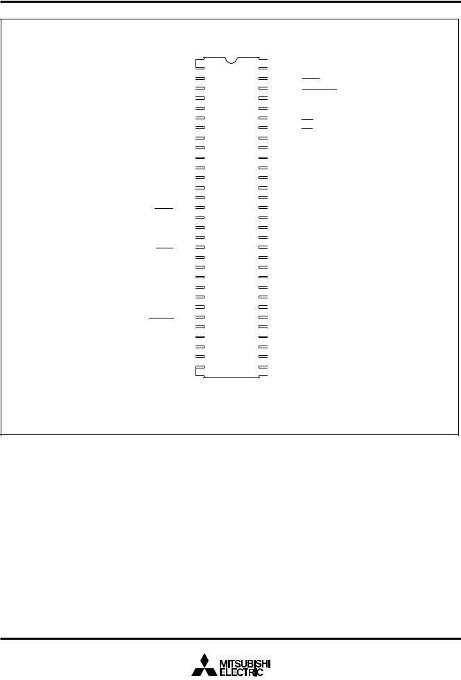
PIN CONFIGURATION (TOP VIEW)
P37/RD 

P36/WR 

P35/SYNC 

P34/φ 

P33/RESETOUT 

P32/ONW 

P31/DA2
P30/DA1
VCC
VREF
AVSS
P67/AN7 

P66/AN6 

P65/AN5 

P64/AN4 

P63 /AN3 

P00/AD0 |
P01/AD1 |
P02/AD2 |
P03/AD3 |
P04/AD4 |
P05/AD5 |
P06/AD6 |
|
P07/AD7 |
P10/AD8 |
P11/AD9 |
P12/AD10 |
|
P13/AD11 |
P14/AD12 |
P15/AD13 |
P16/AD14 |
P17/AD15 |
|
|
|
|
|
||||||||||||||||
|
|
|
|
|
|
|
|
|
|
|
|
|
|
|
|
|
|
|
|
|
|
|
|
|
|
|
|
|
|
|
|
|
|
|
|
|
|
|
|
|
|
|
|
|
|
|
|
|
|
|
|
|
|
|
|
|
|
|
|
|
|
|
|
|
|
|
|
|
|
|
|
|
|
|
|
|
|
48 |
47 |
46 |
45 |
44 |
43 |
42 |
41 |
40 |
39 |
38 |
37 |
36 |
35 |
34 |
33 |
|
|
|
|
|
||||||||||||||||||
49 |
|
|
|
|
|
|
|
|
|
|
|
|
|
|
|
|
|
|
|
|
|
|
|
|
|
|
|
|
|
|
|
32 |
|
|
|
|
P20/DB0 |
|
|
|
|
|
|
|
|
|
|
|
|
|
|
|
|
|
|
|
|
|
|
|
|
|
|
|
|
|
|
|
|
|
|
|
|||||
50 |
|
|
|
|
|
|
|
|
|
|
|
|
|
|
|
|
|
|
|
|
|
|
|
|
|
|
|
|
|
|
|
31 |
|
|
|
|
P21/DB1 |
|
|
|
|
|
|
|
|
|
|
|
|
|
|
|
|
|
|
|
|
|
|
|
|
|
|
|
|
|
|
|
|
|
|
|
|
||||
51 |
|
|
|
|
|
|
|
|
|
|
|
|
|
|
|
|
|
|
|
|
|
|
|
|
|
|
|
|
|
|
|
30 |
|
|
|
|
P22/DB2 |
|
|
|
|
|
|
|
|
|
|
|
|
|
|
|
|
|
|
|
|
|
|
|
|
|
|
|
|
|
|
|
|
|
|
|
|
||||
52 |
|
|
|
|
|
|
|
|
|
|
|
|
|
|
|
|
|
|
|
|
|
|
|
|
|
|
|
|
|
|
|
29 |
|
|
|
|
P23/DB3 |
|
|
|
|
|
|
|
|
|
|
|
|
|
|
|
|
|
|
|
|
|
|
|
|
|
|
|
|
|
|
|
|
|
|
|
|
||||
53 |
|
|
|
|
|
|
|
|
|
|
|
|
|
|
|
|
|
|
|
|
|
|
|
|
|
|
|
|
|
|
|
28 |
|
|
|
|
P24/DB4 |
|
54 |
|
|
|
|
|
|
|
|
|
|
|
|
|
|
|
|
|
|
|
|
|
|
|
|
|
|
|
|
|
|
|
27 |
|
|
|
|
P25/DB5 |
|
|
|
|
|
|
|
|
|
|
|
|
|
|
|
|
|
|
|
|
|
|
|
|
|
|
|
|
|
|
|
|
|
|
|
|
||||
55 |
|
|
|
|
|
|
|
|
|
|
|
|
|
|
|
|
|
|
|
|
|
|
|
|
|
|
|
|
|
|
|
26 |
|
|
|
|
P26/DB6 |
|
|
|
|
|
|
|
|
|
|
|
|
|
|
|
|
|
|
|
|
|
|
|
|
|
|
|
|
|
|
|
|
|
|
|
|
||||
56 |
|
|
|
|
|
M38022M4-XXXFP |
|
|
|
|
25 |
|
|
|
|
P27/DB7 |
||||||||||||||||||||||
|
|
|
|
|
|
|
|
|
|
|
|
|
||||||||||||||||||||||||||
57 |
|
|
|
|
|
|
|
|
|
24 |
|
|
|
|
VSS |
|||||||||||||||||||||||
58 |
|
|
|
|
|
|
|
|
|
|
|
|
|
|
|
|
|
|
|
|
|
|
|
|
|
|
|
|
|
|
|
23 |
|
|
|
|
XOUT |
|
59 |
|
|
|
|
|
|
|
|
|
|
|
|
|
|
|
|
|
|
|
|
|
|
|
|
|
|
|
|
|
|
|
22 |
|
|
|
|
XIN |
|
|
|
|
|
|
|
|
|
|
|
|
|
|
|
|
|
|
|
|
|
|
|
|
|
|
|
|
|
|
|
|
|
|
|
|
||||
60 |
|
|
|
|
|
|
|
|
|
|
|
|
|
|
|
|
|
|
|
|
|
|
|
|
|
|
|
|
|
|
|
21 |
|
|
|
|
P40/INT4 |
|
|
|
|
|
|
|
|
|
|
|
|
|
|
|
|
|
|
|
|
|
|
|
|
|
|
|
|
|
|
|
|
|
|
|
|
||||
61 |
|
|
|
|
|
|
|
|
|
|
|
|
|
|
|
|
|
|
|
|
|
|
|
|
|
|
|
|
|
|
|
20 |
|
|
|
|
P41/INT0 |
|
|
|
|
|
|
|
|
|
|
|
|
|
|
|
|
|
|
|
|
|
|
|
|
|
|
|
|
|
|
|
|
|
|
|
|||||
62 |
|
|
|
|
|
|
|
|
|
|
|
|
|
|
|
|
|
|
|
|
|
|
|
|
|
|
|
|
|
|
|
19 |
|
|
|
|
RESET |
|
|
|
|
|
|
|
|
|
|
|
|
|
|
|
|
|
|
|
|
|
|
|
|
|
|
|
|
|
|
|
|
|
|
|
|
||||
63 |
|
|
|
|
|
|
|
|
|
|
|
|
|
|
|
|
|
|
|
|
|
|
|
|
|
|
|
|
|
|
|
18 |
|
|
|
|
CNVSS |
|
|
|
|
|
|
|
|
|
|
|
|
|
|
|
|
|
|
|
|
|
|
|
|
|
|
|
|
|
|
|
|
|
|
|
|
||||
64 |
|
|
|
|
|
|
|
|
|
|
|
|
|
|
|
|
|
|
10 |
11 |
12 |
13 |
|
|
15 |
17 |
|
|
|
|
P42/INT1 |
|||||||
|
|
|
|
|
|
|
|
|
|
|
|
|
|
|
|
|
|
|
|
|
|
|
|
|||||||||||||||
1 |
2 |
3 |
4 |
5 |
6 |
7 |
8 |
9 |
14 |
16 |
|
|
|
|
|
|||||||||||||||||||||||
|
|
|
|
|
|
|
|
|
|
|
|
|
|
|
|
|
|
|
|
|
|
|
|
|
|
|
|
|
|
|
|
|
|
|
|
|
|
|
|
|
|
|
|
|
|
|
|
|
|
|
|
|
|
|
|
|
|
|
|
|
|
|
|
|
|
|
|
|
|
|
|
|
|
|
|
|
|
P62/AN2 |
P61/AN1 |
P60/AN0 |
P57/INT3 |
P56/PWM |
P55/CNTR1 |
P54/CNTR0 |
|
P53/SRDY2 |
P52/SCLK2 |
P51/SOUT2 |
P50/SIN2 |
|
P47/SRDY1 |
P46/SCLK1 |
P45/TXD |
P44/RXD |
P43/INT2 |
|
|
|
|
|
||||||||||||||||
|
|
|
|
|
|
|
||||||||||||||||||||||||||||||||
|
|
|
|
|
|
|
||||||||||||||||||||||||||||||||
Package type : 64P6N-A 64-pin plastic-molded QFP
MITSUBISHI MICROCOMPUTERS
3802 Group
SINGLE-CHIP 8-BIT CMOS MICROCOMPUTER
PIN CONFIGURATION (TOP VIEW)
VCC 1
VREF 
 2
2
AVSS 
 3
3
P67/AN7 

 4
4
P66/AN6 

 5
5
P65/AN5 

 6
6
P64/AN4 

 7
7
P63/AN3 

 8
8
P62/AN2 

 9
9
P61/AN1 

 10
10
P60/AN0 

 11
11
P57/INT3 

 12
12
P56/PWM 

 13
13
P55/CNTR1 

 14
14
P54/CNTR0 

 15
15
P53/SRDY2 

 16
16
P52/SCLK2 

 17
17
P51/SOUT2 

 18
18
P50/SIN2 

 19
19
P47/SRDY1 

 20
20
P46/SCLK1 

 21
21
P45/TXD 

 22 P44/RXD

 23 P43/INT2

 24 P42/INT1

 25
25
CNVSS 
 26
26
RESET 
 27 P41/INT0

 28 P40/INT4

 29
29
XIN 
 30 XOUT
 31
31
VSS 32
XXXSP-M38022M4
64


63


62


61


60


59


58


57


56


55


54


53


52


51


50


49


48


47


46


45


44


43


42


41


40


39


38


37


36


35


34


33


P30/DA1
P31/DA2
P32/ONW
P33/RESETOUT
P34/φ
P35/SYNC
P36/WR
P37/RD
P00/AD0
P01/AD1
P02/AD2
P03/AD3
P04/AD4
P05/AD5
P06/AD6
P07/AD7
P10/AD8
P11/AD9
P12/AD10
P13/AD11
P14/AD12
P15/AD13
P16/AD14
P17/AD15
P20/DB0
P21/DB1
P22/DB2
P23/DB3
P24/DB4
P25/DB5
P26/DB6
P27/DB7
Package type : 64P4B 64-pin shrink plastic-molded DIP
2

FUNCTIONAL BLOCK DIAGRAM (Package : 64P4B)
Clock input |
Clock output |
|
|
Reset input |
|
|
VSS |
VCC |
RESET |
CNVSS |
|||
XIN |
XOUT |
|||||
30 |
31 |
32 |
1 |
27 |
26 |
Clock generating circuit
|
Timer 1 (8) |
Prescaler 12 (8) |
Timer 2 (8) |
Prescaler X (8) |
Timer X (8) |
Prescaler Y (8) |
Timer Y (8) |
A-D |
|
|
D-A |
D-A |
converter |
PWM (8) |
SI/O2 (8) SI/O1 (8) |
converter 2 |
converter 1 |
(8) |
(8) |
(8) |
INT0
|
|
|
~ |
|
|
|
|
INT3 |
|
INT2 |
|
|
|
|
|
|
INT4 |
|
|
|
P6(8) |
P5(8) |
P4(8) |
P3(8) |
P2(8) |
P1(8) |
P0(8) |
2 |
3 |
4 |
5 |
6 |
7 |
8 |
9 10 11 |
12 13 14 15 16 17 18 19 |
20 21 22 23 24 25 28 29 |
57 58 59 60 61 62 63 64 |
33 34 35 36 37 38 39 40 |
41 42 43 44 45 46 47 48 |
49 50 51 52 53 54 55 56 |
VREF AVSS
I/O port P6 |
I/O port P5 |
I/O port P4 |
I/O port P3 |
I/O port P2 |
I/O port P1 |
I/O port P0 |
3
MICROCOMPUTER CMOS BIT-8 CHIP-SINGLE
Group 3802 |
MICROCOMPUTERS MITSUBISHI |

|
|
|
|
|
|
|
|
|
|
MITSUBISHI MICROCOMPUTERS |
|
|
|
|
|
|
|
|
|
|
3802 Group |
|
|
|
|
|
|
|
SINGLE-CHIP 8-BIT CMOS MICROCOMPUTER |
|||
|
|
|
|
|
|
|
|
|
|
|
PIN DESCRIPTION |
|
|
|
|
||||||
|
|
|
|
|
|
|
|
|
|
|
|
|
Pin |
Name |
Function |
|
|
|
|||
|
|
Function except a port function |
||||||||
|
|
|
|
|
|
|
|
|
|
|
|
|
|
|
|
|
|
|
|
|
|
|
VCC, VSS |
Power source |
• Apply voltage of 3.0 V–5.5 V to VCC, and 0 V to VSS. |
|
||||||
|
|
|
|
|
|
|
(Extended operating temperature version : 4.0 V to 5.5 V) |
|||
|
|
|
|
|
|
|
|
|
|
|
|
CNVSS |
CNVSS |
• This pin controls the operation mode of the chip. |
|
||||||
|
|
|
|
|
|
|
• Normally connected to VSS. |
|
||
|
|
|
|
|
|
|
• If this pin is connected to VCC, the internal ROM is inhibited and external memory is accessed. |
|||
|
|
|
|
|
|
|
|
|
|
|
|
VREF |
Analog reference |
• Reference voltage input pin for A-D and D-A converters |
|
||||||
|
|
|
|
|
|
voltage |
|
|
|
|
|
|
|
|
|
|
|
|
|
|
|
|
AVSS |
Analog power |
• GND input pin for A-D and D-A converters |
|
||||||
|
|
|
|
|
|
source |
• Connect to VSS. |
|
||
|
|
|
|
|
|
|
|
|
|
|
|
|
|
|
|
|
|
|
|
||
|
RESET |
Reset input |
• Reset input pin for active “L” |
|
||||||
|
|
|
|
|
|
|
|
|
|
|
|
XIN |
Clock input |
• Input and output signals for the clock generating circuit. |
|
||||||
|
|
|
|
|
|
|
• Connect a ceramic resonator or quartz-crystal oscillator between the XIN and XOUT pins to set the |
|||
|
|
|
|
|
|
|
||||
|
XOUT |
Clock output |
oscillation frequency. |
|
||||||
|
|
|
|
|
|
|
• If an external clock is used, connect the clock source to the XIN pin and leave the XOUT pin open. |
|||
|
|
|
|
|
|
|
• The clock is used as the oscillating source of system clock. |
|||
|
|
|
|
|
|
|
|
|
|
|
|
P00–P07 |
I/O port P0 |
• 8 bit CMOS I/O port |
|
||||||
|
|
|
|
|
|
|
• I/O direction register allows each pin to be individually programmed as either input or output. |
|||
|
|
|
|
|
|
|
||||
|
P10–P17 |
I/O port P1 |
• At reset this port is set to input mode. |
|
||||||
|
|
|
|
|
|
|
• In modes other than single-chip, these pins are used as address, data, and control bus I/O pins. |
|||
|
|
|
|
|
|
|
||||
|
P20–P27 |
I/O port P2 |
• CMOS compatible input level |
|
||||||
|
|
|
|
|
|
|
• CMOS 3-state output structure |
|
||
|
P30/DA1, |
I/O port P3 |
• D–A conversion output pins |
|||||||
|
|
|
|
|||||||
|
P31/DA2 |
|
|
|
|
|
||||
|
|
|
|
|
|
|
|
|
|
|
|
P32–P37 |
|
|
|
|
|
||||
|
|
|
|
|
|
|
|
|
|
|
|
P40/INT4, |
I/O port P4 |
• 8-bit CMOS I/O port with the same function as port P0 |
|
• External interrupt input pin |
|||||
|
P41/INT0, |
|
• CMOS compatible input level |
|
|
|||||
|
P42/INT1, |
|
• CMOS 3-state output structure |
|
|
|||||
|
P43/INT2 |
|
|
|
|
|
||||
|
|
|
|
|
|
|
|
|
|
|
|
P44/RXD, |
|
|
|
|
• Serial I/O1 I/O pins |
||||
|
P45/TXD, |
|
|
|
|
|
||||
|
P46/SCLK1, |
|
|
|
|
|
||||
|
|
|
|
|
|
|
|
|
|
|
|
P47/SRDY1 |
|
|
|
|
|
||||
|
|
|
|
|
|
|
|
|
|
|
|
P50/SIN2, |
I/O port P5 |
• 8-bit CMOS I/O port with the same function as port P0 |
|
• Serial I/O2 I/O pins |
|||||
|
P51/SOUT2, |
|
• CMOS compatible input level |
|
|
|||||
|
P52/SCLK2, |
|
• CMOS 3-state output structure |
|
|
|||||
|
|
|
|
|
|
|
|
|
||
|
P53/SRDY2 |
|
|
|
|
|
||||
|
|
|
|
|
|
|
|
|
|
|
|
P54/CNTR0, |
|
|
|
|
• Timer X and Timer Y I/O pins |
||||
|
P55/CNTR1 |
|
|
|
|
|
||||
|
|
|
|
|
|
|
|
|
|
|
|
P56/PWM |
|
|
|
|
• PWM output pin |
||||
|
|
|
|
|
|
|
|
|
|
|
|
P57/INT3 |
|
|
|
|
• External interrupt input pin |
||||
|
|
|
|
|
|
|||||
|
P60/AN0– |
I/O port P6 |
• 8-bit CMOS I/O port with the same function as port P0 |
|
• A-D conversion input pins |
|||||
|
P67/AN7 |
|
• CMOS compatible input level |
|
|
|||||
|
|
|
|
|
|
|
• CMOS 3-state output structure |
|
|
|
|
|
|
|
|
|
|
|
|
|
|
4

MITSUBISHI MICROCOMPUTERS
3802 Group
SINGLE-CHIP 8-BIT CMOS MICROCOMPUTER
GROUP EXPANSION |
|
|
|
|
|
|
|
(2) |
Packages |
|
|
|
|
|||||||||
Mitsubishi plans to expand the 3802 group as follows: |
|
|
|
|
|
64P4B |
............................................ |
|
|
Shrink plastic molded DIP |
||||||||||||
(1) Support for mask ROM, One Time PROM, and EPROM |
|
|
64P6N-A ................................................... |
|
|
Plastic molded QFP |
||||||||||||||||
versions |
|
|
|
|
|
|
|
|
|
|
|
|
64S1B-E .................................................... |
|
|
Shrink ceramic DIP |
||||||
ROM/PROM capacity ................................... |
|
|
|
8 K to 32 K bytes |
|
|
64D0 ................................................................... |
|
|
|
|
Ceramic LCC |
||||||||||
RAM capacity .............................................. |
|
|
|
|
|
384 to 1024 bytes |
|
|
|
|
|
|
|
|
|
|
||||||
|
|
|
|
|
|
|
|
|
|
|
|
|
|
|
|
|
|
|
|
|
|
|
Memory Expansion Plan |
|
|
|
|
|
|
|
|
|
|
|
|
|
|
|
|
|
|||||
|
|
|
|
|
|
|
|
|
|
|
|
|
|
|
|
|
||||||
ROM size (bytes) |
|
|
|
|
|
|
|
|
|
|
|
|
Mass product |
|
|
|
||||||
32K |
|
|
|
|
|
|
|
|
|
|
|
|
|
|
|
|
|
|
M38027M8/E8 |
|
|
|
|
|
|
|
|
|
|
|
|
|
|
|
|
|
|
|
|
|
|
||||
28K |
|
|
|
|
|
|
|
|
|
|
|
|
|
|
|
|
|
|
|
|
|
|
|
|
|
|
|
|
|
|
|
|
|
|
|
|
|
|
|
|
|
|
|
|
|
|
|
|
|
|
|
|
|
|
|
|
Mass product |
|
|
|
|
|
|
|
|
|
|
|
24K |
|
|
|
|
|
|
|
|
|
|
|
M38024M6 |
|
|
|
|
|
|
|
|
||
20K |
|
|
|
|
|
|
|
|
|
|
|
|
|
|
|
|
|
|
|
|
|
|
|
|
|
|
|
|
|
|
|
|
|
|
|
|
|
|
|
|
|
|
|
|
|
|
|
|
|
Mass product |
|
|
|
|
|
|
|
|
|
|
|
|
|
|
|
|
||
16K |
|
|
|
|
|
|
M38022M4 |
|
|
|
|
|
|
|
|
|
|
|||||
12K |
|
|
|
|
|
|
|
|
|
|
|
|
|
|
|
|
|
|
|
|
|
|
|
|
|
|
|
|
|
|
|
|
|
|
|
|
|
|
|
|
|
|
|
|
|
|
|
|
|
Mass product |
|
|
|
|
|
|
|
|
|
|
|
|
|
|
|
|
||
8K |
|
|
|
|
|
|
M38022M2 |
|
|
|
|
|
|
|
|
|
|
|||||
4K |
|
|
|
|
|
|
|
|
|
|
|
|
|
|
|
|
|
|
|
|
|
|
|
|
|
|
|
|
|
|
|
|
|
|
|
|
|
|
|
|
|
|
|||
|
|
|
|
|
|
|
|
|
|
|
|
|
|
|
|
|
|
|
|
|
|
|
|
|
|
192 |
256 |
|
384 |
512 |
|
640 |
768 |
896 |
1024 |
|
|
||||||||
|
|
|
|
|
|
|
|
|
|
RAM size (bytes) |
|
|
|
|
|
|
|
|
|
|
||
|
|
|
|
|
|
|
|
|
|
|
|
|
|
|
|
|
|
|||||
Currently supported products are listed below |
|
|
|
|
|
|
|
|
|
|
|
As of May 1996 |
||||||||||
|
|
|
|
|
|
|
|
|
|
|
|
|
|
|
|
|
|
|
|
|
|
|
Product |
(P) ROM size (bytes) |
|
RAM size (bytes) |
|
Package |
|
|
|
|
Remarks |
|
|||||||||||
ROM size for User in ( |
) |
|
|
|
|
|
|
|
||||||||||||||
|
|
|
|
|
|
|
|
|
|
|
|
|
|
|
|
|
|
|||||
|
|
|
|
|
|
|
|
|
|
|
|
|
|
|
|
|
|
|
|
|||
M38022M2-XXXSP |
8192 |
|
|
|
|
384 |
|
|
64P4B |
|
Mask ROM version |
|
||||||||||
M38022M2-XXXFP |
(8062) |
|
|
|
|
|
|
64P6N-A |
|
Mask ROM version |
|
|||||||||||
|
|
|
|
|
|
|
|
|
|
|||||||||||||
M38022M4-XXXSP |
16384 |
|
|
|
|
384 |
|
|
64P4B |
|
Mask ROM version |
|
||||||||||
M38022M4-XXXFP |
(16254) |
|
|
|
|
|
|
64P6N-A |
|
Mask ROM version |
|
|||||||||||
|
|
|
|
|
|
|
|
|
|
|||||||||||||
|
|
|
|
|
|
|
|
|
|
|
|
|
||||||||||
|
|
|
|
|
|
|
|
|
|
|
|
|
|
|
|
|
|
|
|
|||
M38024M6-XXXSP |
24576 |
|
|
|
|
640 |
|
|
64P4B |
|
Mask ROM version |
|
||||||||||
M38024M6-XXXFP |
(24446) |
|
|
|
|
|
|
64P6N-A |
|
Mask ROM version |
|
|||||||||||
|
|
|
|
|
|
|
|
|
|
|||||||||||||
|
|
|
|
|
|
|
|
|
|
|
|
|
|
|
|
|
|
|
|
|
||
M38027M8-XXXSP |
|
|
|
|
|
|
|
|
|
|
|
|
|
|
Mask ROM version |
|
||||||
|
|
|
|
|
|
|
|
|
|
|
|
|
|
|
|
|
|
|
||||
M38027E8-XXXSP |
|
|
|
|
|
|
|
|
|
|
|
64P4B |
One Time PROM version |
|
||||||||
M38027E8SP |
|
|
|
|
|
|
|
|
|
|
|
|
|
|
One Time PROM version (blank) |
|
||||||
|
|
|
|
|
|
|
|
|
|
|
|
|
|
|
|
|
|
|
|
|
||
M38027M8-XXXFP |
32768 |
|
|
|
|
1024 |
|
|
|
|
|
Mask ROM version |
|
|||||||||
M38027E8-XXXFP |
(32638) |
|
|
|
|
|
|
64P6N-A |
One Time PROM version |
|
||||||||||||
|
|
|
|
|
|
|
|
|
||||||||||||||
M38027E8FP |
|
|
|
|
|
|
|
|
|
|
|
|
|
|
One Time PROM version (blank) |
|
||||||
|
|
|
|
|
|
|
|
|
|
|
|
|
|
|
|
|
|
|
|
|||
M38027E8SS |
|
|
|
|
|
|
|
|
|
|
|
64S1B-E |
|
EPROM version |
|
|||||||
|
|
|
|
|
|
|
|
|
|
|
|
|
|
|
|
|
|
|
|
|||
M38027E8FS |
|
|
|
|
|
|
|
|
|
|
|
64D0 |
|
EPROM version |
|
|||||||
5

MITSUBISHI MICROCOMPUTERS
3802 Group
SINGLE-CHIP 8-BIT CMOS MICROCOMPUTER
GROUP EXPANSION
(Extended operating temperature version)
Mitsubishi plans to expand the 3802 group (extended operating temperature version) as follows:
(1)Support for mask ROM One Time PROM, and EPROM versions
ROM/PROM capacity ................................... |
8 K to 32 K bytes |
RAM capacity .............................................. |
384 to 1024 bytes |
(2) Packages |
|
64P4B ............................................ |
Shrink plastic molded DIP |
64P6N-A ................................................... |
Plastic molded QFP |
Memory Expansion Plan (Extended operating temperature version)
ROM size (bytes) |
|
|
|
|
|
Mass product |
|
32K |
|
|
|
|
|
|
M38027M8D/E8D |
28K |
|
|
|
|
|
|
|
24K |
|
|
|
|
|
|
|
20K |
|
|
|
|
|
|
|
Mass product |
|
|
|
|
|
||
16K |
|
M38022M4D |
|
|
|
|
|
12K |
|
|
|
|
|
|
|
Mass product |
|
|
|
|
|
||
8K |
|
M38022M2D |
|
|
|
|
|
4K |
|
|
|
|
|
|
|
192 |
256 |
384 |
512 |
640 |
768 |
896 |
1024 |
|
|
RAM size (bytes) |
|
|
|
|
|
Currently supported products are listed below. |
|
As of May 1996 |
|||
|
|
|
|
|
|
Product |
(P) ROM size (bytes) |
RAM size (bytes) |
Package |
Remarks |
|
M38022M2DXXXSP |
8192 |
384 |
64P4B |
Mask ROM version |
|
M38022M2DXXXFP |
(8062) |
64P6N-A |
Mask ROM version |
||
|
|||||
M38022M4DXXXSP |
16384 |
384 |
64P4B |
Mask ROM version |
|
M38022M4DXXXFP |
(16254) |
64P6N-A |
Mask ROM version |
||
|
|||||
M38027M8DXXXSP |
|
|
|
Mask ROM version |
|
M38027E8DXXXSP |
|
|
64P4B |
One Time PROM version |
|
M38027E8DSP |
32768 |
1024 |
|
One Time PROM version (blank) |
|
M38027M8DXXXFP |
(32638) |
|
Mask ROM version |
||
|
|
||||
|
|
|
|
|
|
M38027E8DXXXFP |
|
|
64P6N-A |
One Time PROM version |
|
|
|
|
|
|
|
M38027E8DFP |
|
|
|
One Time PROM version (blank) |
|
6
MITSUBISHI MICROCOMPUTERS
3802 Group
SINGLE-CHIP 8-BIT CMOS MICROCOMPUTER
PART NUMBERING
Product M3802 2 M 4 - XXX SP
 Package type
SP : 64P4B package
FP : 64P6N-A package
SS : 64S1B-E package
FS : 64D0 package
ROM number
Omitted in some types.
Normally, using hyphen.
When electrical characteristic, or division of quality identification code using alphanumeric character
– : standard
D : Extended operating temperature version
ROM/PROM size 1 : 4096 bytes 2 : 8192 bytes
3 : 12288 bytes
4 : 16384 bytes
5 : 20480 bytes
6 : 24576 bytes
7 : 28672 bytes
8 : 32768 bytes
The first 128 bytes and the last 2 bytes of ROM are reserved areas ; they cannot be used.
Memory type
M : Mask ROM version
E : EPROM or One Time PROM version
RAM size
0 : 192 bytes
1 : 256 bytes
2 : 384 bytes
3 : 512 bytes
4 : 640 bytes
5 : 768 bytes
6 : 896 bytes
7 : 1024 bytes
7

MITSUBISHI MICROCOMPUTERS
3802 Group
SINGLE-CHIP 8-BIT CMOS MICROCOMPUTER
FUNCTIONAL DESCRIPTION
Central Processing Unit (CPU)
The 3802 group uses the standard 740 family instruction set. Refer to the table of 740 family addressing modes and machine instructions or the SERIES 740 <Software> User’s Manual for details on the instruction set.
Machine-resident 740 family instructions are as follows:
The FST and SLW instruction cannot be used.
The STP, WIT, MUL, and DIV instruction can be used.
CPU mode register
The CPU mode register is allocated at address 003B16.
The CPU mode register contains the stack page selection bit.
b7 |
|
b0 |
|
|
||||||||||||||||
|
|
|
|
|
|
|
|
|
|
|
|
|
|
|
|
CPU mode register |
||||
|
|
|
|
|
|
|
|
|
|
|
|
|
|
|
|
(CPUM : address 003B16) |
||||
|
|
|
|
|
|
|
|
|
|
|
|
|
|
|
|
|||||
|
|
|
|
|
|
|
|
|
|
|
|
|
|
|
|
|
|
Processor mode bits |
||
|
|
|
|
|
|
|
|
|
|
|
|
|
|
|
|
|
||||
|
|
|
|
|
|
|
|
|
|
|
|
|
|
|
|
|
|
b1 b0 |
|
|
|
|
|
|
|
|
|
|
|
|
|
|
|
0 |
0 |
: Single-chip mode |
|||||
|
|
|
|
|
|
|
|
|
|
|
|
|
0 |
1 |
: Memory expansion mode |
|||||
|
|
|
|
|
|
|
|
|
|
|
|
|
1 |
0 |
: Microprocessor mode |
|||||
|
|
|
|
|
|
|
|
|
|
|
|
|
1 |
1 |
: Not available |
|||||
|
|
|
|
|
|
|
|
|
|
|
|
|
|
|
|
|
|
Stack page selection bit |
||
|
|
|
|
|
|
|
|
|
|
|
|
|
|
|
|
|
|
|||
|
|
|
|
|
|
|
|
|
|
|
|
|
0 |
: 0 page |
||||||
|
|
|
|
|
|
|
|
|
|
|
|
|
1 |
: 1 page |
||||||
|
|
|
|
|
|
|
|
|
|
|
|
|
|
|
|
|
|
Not used (return “0” when read) |
||
|
|
|
|
|
|
|
|
|
|
|
|
|
|
|
|
|
|
|||
Fig. 1 Structure of CPU mode register
8

MITSUBISHI MICROCOMPUTERS
3802 Group
SINGLE-CHIP 8-BIT CMOS MICROCOMPUTER
Memory
Special function register (SFR) area
The Special Function Register area in the zero page contains control registers such as I/O ports and timers.
RAM
RAM is used for data storage and for stack area of subroutine calls and interrupts.
Zero page
The 256 bytes from addresses 000016 to 00FF16 are called the zero page area. The internal RAM and the special function registers (SFR) are allocated to this area.
The zero page addressing mode can be used to specify memory and register addresses in the zero page area. Access to this area with only 2 bytes is possible in the zero page addressing mode.
ROM
The first 128 bytes and the last 2 bytes of ROM are reserved for device testing and the rest is user area for storing programs.
Interrupt vector area
The interrupt vector area contains reset and interrupt vectors.
Special page
The 256 bytes from addresses FF0016 to FFFF16 are called the special page area. The special page addressing mode can be used to specify memory addresses in the special page area. Access to this area with only 2 bytes is possible in the special page addressing mode.
RAM area
RAM capacity |
Address |
|
000016 |
|
|
|
|
||||
|
|
|
|
|
|||||||
(bytes) |
XXXX16 |
|
SFR area |
|
|
|
|||||
|
|
|
|
|
|
|
|
|
|||
|
|
|
|
|
|
|
|
|
|
|
|
192 |
00FF16 |
|
|
|
|
|
|
|
|
|
Zero page |
256 |
013F16 |
|
|
004016 |
|
|
|
|
|||
|
|
|
|
|
|
|
|
|
|
||
384 |
01BF16 |
|
|
010016 |
|
|
|
|
|||
|
|
|
|
|
|
|
|
||||
512 |
023F16 |
|
|
|
|
|
|||||
|
RAM |
|
|
|
|
|
|
|
|
||
640 |
02BF16 |
|
|
|
|
|
|
|
|
|
|
|
|
|
|
|
|
|
|
|
|
||
768 |
033F16 |
|
|
|
|
|
|
|
|
|
|
896 |
03BF16 |
|
|
|
|
|
XXXX16 |
|
|
|
|
1024 |
043F16 |
|
|
|
|
|
|
|
|
|
|
|
|
|
|
|
|
|
|
Reserved area |
|
|
|
ROM area |
|
|
044016 |
|
|
|
|
||||
|
|
Not used |
|
|
|
||||||
|
|
|
|
|
|
|
|
|
|
||
ROM capacity |
Address |
Address |
|
|
|
|
|
|
|
|
|
(bytes) |
YYYY16 |
ZZZZ16 |
|
|
|
|
YYYY16 |
Reserved ROM area |
|
|
|
4096 |
F00016 |
F08016 |
|
|
|
|
|
|
|
|
|
8192 |
E00016 |
E08016 |
|
|
|
|
|
(128 bytes) |
|
|
|
|
|
|
|
|
|
|
|
|
|||
12288 |
D00016 |
D08016 |
|
|
|
|
ZZZZ16 |
|
|
|
|
|
|
|
|
|
|
|
|
||||
16384 |
C00016 |
C08016 |
|
|
|
|
|
|
|
|
|
20480 |
B00016 |
B08016 |
|
|
|
|
|
|
|
|
|
24576 |
A00016 |
A08016 |
|
|
|
|
|
|
|
|
|
28672 |
900016 |
908016 |
ROM |
|
|
|
|
|
|||
32768 |
800016 |
808016 |
|
|
|
|
|||||
|
|
|
|
FF0016 |
|
|
|
|
|||
|
|
|
|
|
|
|
|
|
|
|
|
|
|
|
|
|
|
|
FFDC16 |
|
|
|
Special page |
|
|
|
Interrupt vector area |
|
|
||||||
|
|
|
|
|
|
|
|
|
|
||
|
|
|
|
|
|
|
|
|
|
|
|
|
|
|
|
|
|
|
FFFE16 |
|
|
|
|
|
|
|
Reserved ROM area |
|
|
|
|||||
|
|
|
|
|
|
|
FFFF16 |
|
|
|
|
Fig. 2 Memory map diagram
9

|
|
|
MITSUBISHI MICROCOMPUTERS |
|
|
|
|
|
3802 Group |
|
|
|
SINGLE-CHIP 8-BIT CMOS MICROCOMPUTER |
|
|
|
|
|
|
|
|
|
|
|
|
|
|
|
|
000016 |
Port P0 (P0) |
002016 |
Prescaler 12 (PRE12) |
|
|
|
|
|
|
000116 |
Port P0 direction register (P0D) |
002116 |
Timer 1 (T1) |
|
|
|
|
|
|
000216 |
Port P1 (P1) |
002216 |
Timer 2 (T2) |
|
|
|
|
|
|
000316 |
Port P1 direction register (P1D) |
002316 |
Timer XY mode register (TM) |
|
|
|
|
|
|
000416 |
Port P2 (P2) |
002416 |
Prescaler X (PREX) |
|
|
|
|
|
|
000516 |
Port P2 direction register (P2D) |
002516 |
Timer X (TX) |
|
|
|
|
|
|
000616 |
Port P3 (P3) |
002616 |
Prescaler Y (PREY) |
|
|
|
|
|
|
000716 |
Port P3 direction register (P3D) |
002716 |
Timer Y (TY) |
|
|
|
|
|
|
000816 |
Port P4 (P4) |
002816 |
|
|
|
|
|
|
|
000916 |
Port P4 direction register (P4D) |
002916 |
|
|
|
|
|
|
|
000A16 |
Port P5 (P5) |
002A16 |
|
|
|
|
|
|
|
000B16 |
Port P5 direction register (P5D) |
002B16 |
PWM control register (PWMCON) |
|
|
|
|
|
|
000C16 |
Port P6 (P6) |
002C16 |
PMW prescaler (PREPWM) |
|
|
|
|
|
|
000D16 |
Port P6 direction register (P6D) |
002D16 |
PWM register (PWM) |
|
000E16 |
|
002E16 |
|
|
|
|
|
||
000F16 |
|
002F16 |
|
|
|
|
|
||
001016 |
|
003016 |
|
|
|
|
|
||
001116 |
|
003116 |
|
|
|
|
|
||
001216 |
|
003216 |
|
|
|
|
|
||
001316 |
|
003316 |
|
|
|
|
|
||
|
|
|
|
|
001416 |
|
003416 |
AD/DA control register (ADCON) |
|
|
|
|
|
|
001516 |
|
003516 |
A-D conversion register (AD) |
|
|
|
|
|
|
001616 |
|
003616 |
D-A1 conversion register (DA1) |
|
|
|
|
|
|
001716 |
|
003716 |
D-A2 conversion register (DA2) |
|
|
|
|
|
|
001816 |
Transmit/Receive buffer register (TB/RB) |
003816 |
|
|
|
|
|
|
|
001916 |
Serial I/O1 status register (SIO1STS) |
003916 |
|
|
|
|
|
|
|
001A16 |
Serial I/O1 control register (SIO1CON) |
003A16 |
Interrupt edge selection register (INTEDGE) |
|
|
|
|
|
|
001B16 |
UART control register (UARTCON) |
003B16 |
CPU mode register (CPUM) |
|
|
|
|
|
|
001C16 |
Baud rate generator (BRG) |
003C16 |
Interrupt request register 1(IREQ1) |
|
|
|
|
|
|
001D16 |
Serial I/O2 control register (SIO2CON) |
003D16 |
Interrupt request register 2(IREQ2) |
|
|
|
|
|
|
001E16 |
|
003E16 |
Interrupt control register 1(ICON1) |
|
|
|
|
|
|
001F16 |
Serial I/O2 register (SIO2) |
003F16 |
Interrupt control register 2(ICON2) |
|
|
|
|
|
|
|
|
|
|
|
Fig. 3 Memory map of special function register (SFR)
10
MITSUBISHI MICROCOMPUTERS
3802 Group
SINGLE-CHIP 8-BIT CMOS MICROCOMPUTER
I/O Ports
Direction registers
The 3802 group has 56 programmable I/O pins arranged in seven
I/O ports (ports P0 to P6). The I/O ports have direction registers which determine the input/output direction of each individual pin.
Each bit in a direction register corresponds to one pin, each pin can be set to be input port or output port.
When “0” is written to the bit corresponding to a pin, that pin becomes an input pin. When “1” is written to that bit, that pin becomes an output pin.
If data is read from a pin which is set to output, the value of the port output latch is read, not the value of the pin itself. Pins set to input are floating. If a pin set to input is written to, only the port output latch is written to and the pin remains floating.
|
|
Pin |
Name |
Input/Output |
I/O Format |
Non-Port Function |
Related SFRs |
Ref.No. |
|||
|
|
|
|
|
|
|
|
|
|
|
|
|
|
|
|
|
Input/output, |
CMOS 3-state output |
Address low-order byte |
|
|
||
P00 |
–P07 |
Port P0 |
CMOS compatible |
CPU mode register |
|
||||||
individual bits |
output |
|
|||||||||
|
|
|
|
|
input level |
|
|
||||
|
|
|
|
|
|
|
|
|
|||
|
|
|
|
|
|
|
|
|
|
|
|
|
|
|
|
|
Input/output, |
CMOS 3-state output |
Address high-order |
|
|
||
P10 |
–P17 |
Port P1 |
CMOS compatible |
CPU mode register |
(1) |
||||||
individual bits |
byte output |
||||||||||
|
|
|
|
|
input level |
|
|
||||
|
|
|
|
|
|
|
|
|
|||
|
|
|
|
|
|
|
|
|
|
|
|
|
|
|
|
|
Input/output, |
CMOS 3-state output |
|
|
|
||
P20 |
–P27 |
Port P2 |
CMOS compatible |
Data bus I/O |
CPU mode register |
|
|||||
individual bits |
|
||||||||||
|
|
|
|
|
input level |
|
|
|
|||
|
|
|
|
|
|
|
|
|
|||
|
|
|
|
|
|
|
|
|
|
||
P30/DA1 |
|
Input/output, |
CMOS 3-state output |
D-A conversion output |
AD/DA control register |
(2) |
|||||
P31/DA2 |
Port P3 |
CMOS compatible |
|
CPU mode register |
|||||||
individual bits |
|
|
|||||||||
|
|
|
|
|
|
|
|
|
|
||
P32 |
–P37 |
|
input level |
Control signal I/O |
CPU mode register |
(1) |
|||||
|
|
||||||||||
|
|
|
|
|
|
|
|
|
|
|
|
P40 |
/INT4, |
|
|
|
|
|
Interrupt edge selection |
|
|||
P41 |
/INT0, |
|
|
|
|
External interrupt input |
(3) |
||||
|
|
|
|
register |
|||||||
P43 |
/INT2 |
|
|
CMOS 3-state output |
|
|
|||||
|
Input/output, |
|
|
|
|||||||
|
|
|
|
|
|
|
|
|
|
||
P44/RXD, |
Port P4 |
CMOS compatible |
|
|
(4) |
||||||
individual bits |
|
Serial I/O1 control |
|||||||||
|
|
|
|
|
|
|
|
|
|||
P45/TXD, |
|
input level |
|
(5) |
|||||||
|
|
Serial I/O1 function I/O |
register |
||||||||
|
|
|
|
|
|
|
|
|
|||
P46 |
/SCLK1, |
|
|
|
|
(6) |
|||||
|
|
|
|
|
UART control register |
||||||
|
|
|
|
|
|
|
|
|
|
||
|
|
|
|
|
|
|
|
|
|
||
P47/SRDY1 |
|
|
|
|
|
(7) |
|||||
|
|
|
|
|
|
||||||
P50 |
/SIN2, |
|
|
|
|
|
|
(8) |
|||
|
|
|
|
|
|
|
|
|
|||
P51 |
/SOUT2, |
|
|
|
|
Serial I/O2 function I/O |
Serial I/O2 control |
(9) |
|||
|
|
|
|
|
|
|
|
|
|
||
P52 |
/SCLK2, |
|
|
CMOS 3-state output |
register |
(10) |
|||||
|
|
|
|||||||||
|
|
|
|
|
|
|
|
|
|||
|
|
|
|
|
|
|
|
|
|||
P53/SRDY2 |
|
Input/output, |
|
|
(11) |
||||||
Port P5 |
CMOS compatible |
|
|
||||||||
|
|
|
|
|
|
|
|
||||
P54 |
/CNTR0, |
individual bits |
Timer X and Timer Y |
|
|
||||||
|
input level |
Timer XY mode register |
(12) |
||||||||
P55 |
/CNTR1 |
|
|
function I/O |
|||||||
|
|
|
|
|
|
||||||
|
|
|
|
|
|
|
|
|
|
|
|
P56 |
/PWM |
|
|
|
|
PWM output |
PWM control register |
(13) |
|||
|
|
|
|
|
|
|
|
|
|||
P57 |
/INT3 |
|
|
|
|
External interrupt input |
Interrupt edge selection register |
(3) |
|||
|
|
|
|
|
|
|
|
|
|
|
|
P60 |
/AN0– |
|
Input/output, |
CMOS 3-state output |
|
|
|
||||
Port P6 |
CMOS compatible |
A-D conversion input |
|
(14) |
|||||||
P67 |
/AN7 |
individual bits |
|
||||||||
|
input level |
|
|
|
|||||||
|
|
|
|
|
|
|
|
|
|||
|
|
|
|
|
|
|
|
|
|
|
|
Note 1: For details of the functions of ports P0 to P3 in modes other than single-chip mode, and how to use double-function ports as function I/O ports, refer to the applicable sections.
2: Make sure that the input level at each pin is either 0 V or VCC during execution of the STP instruction.
When an input level is at an intermediate potential, a current will flow from VCC to VSS through the input-stage gate.
11
MITSUBISHI MICROCOMPUTERS
3802 Group
SINGLE-CHIP 8-BIT CMOS MICROCOMPUTER
(1) Ports P0, P1, P2, P32–P37
 Direction register

Data bus  Port latch
(2) Ports P30, P31
 Direction register

Data bus  Port latch
D–A conversion output |
DA1 output enable bit (P30) DA2 output enable bit (P31)
(3) Ports P40–P43, P57
 Direction register

Data bus  Port latch
Interrupt input |
(4) Port P44
Serial I/O1 enable bit

Receive enable bit
|
Direction register |
Data bus |
Port latch |
|
Serial I/O1 input |
(5) Port P45
P45/TXD P-channel output disable bit 

Serial I/O1 enable bit

Transmit enable bit
|
Direction register |
Data bus |
Port latch |
Serial I/O1 output 

(6) Port P46
Serial I/O1 synchronous clock selection bit 

Serial I/O1 enable bit 
Serial I/O1 mode selection bit
Serial I/O1 enable bit 

|
Direction register |
Data bus |
Port latch |
Serial I/O1 clock output 

Serial I/O1 external  clock input
(7) Port P47 |
(8) Port P50 |
Serial I/O1 mode selection bit
Serial I/O1 enable bit

SRDY1 output enable bit
|
Direction register |
Data bus |
Port latch |
Serial I/O1 ready output 

 Direction register

Data bus  Port latch
Serial I/O2 input |
Fig. 4 Port block diagram (single-chip mode) (1)
12

MITSUBISHI MICROCOMPUTERS
3802 Group
SINGLE-CHIP 8-BIT CMOS MICROCOMPUTER
(9) Port P51
P51/SOUT2 P-channel output disable bit 

Serial I/O2 transmit end signal  Serial I/O2 port selection bit
|
Direction register |
Data bus |
Port latch |
Serial I/O2 output 

(10) Port P52
Serial I/O2
synchronous clock selection bit  Serial I/O2 port selection bit

|
Direction register |
Data bus |
Port latch |
Serial I/O2 clock output 

Serial I/O2 external clock input

(11) Port P53 |
(12) Ports P54, 55 |
|
|
SRDY2 output enable bit |
Direction register |
|
|
|
|
Direction register |
|
|
Data bus |
Port latch |
Data bus |
Port latch |
|
|
|
Pulse output mode |
Serial I/O2 ready output |
Timer output |
|
|
|
|
|
|
CNTR0, CNTR1 |
|
|
Interrupt input |
(13) Port P56
PWM output enable bit
|
Direction register |
Data bus |
Port latch |
PWM output 

(14) Port P6
 Direction register

Data bus  Port latch
A-D conversion input |
Analog input pin selection bit
Fig. 5 Port block diagram (single-chip mode) (2)
13

MITSUBISHI MICROCOMPUTERS
3802 Group
SINGLE-CHIP 8-BIT CMOS MICROCOMPUTER
INTERRUPTS
Interrupts occur by sixteen sources: seven external, eight internal, and one software.
Interrupt control
Each interrupt is controlled by an interrupt request bit, an interrupt enable bit, and the interrupt disable flag except for the software interrupt set by the BRK instruction. An interrupt occurs if the corresponding interrupt request and enable bits are “1” and the interrupt disable flag is “0”.
Interrupt enable bits can be set or cleared by software.
Interrupt request bits can be cleared by software, but cannot be set by software.
The BRK instruction cannot be disabled with any flag or bit. The I (interrupt disable) flag disables all interrupts except the BRK instruction interrupt.
When several interrupts occur at the same time, the interrupts are received according to priority.
Table 1. Interrupt vector addresses and priority
Interrupt operation
When an interrupt is received, the contents of the program counter and processor status register are automatically stored into the stack. The interrupt disable flag is set to inhibit other interrupts from interfering.The corresponding interrupt request bit is cleared and the interrupt jump destination address is read from the vector table into the program counter.
Notes on use
When the active edge of an external interrupt (INT0 to INT4,
CNTR0, or CNTR1) is changed, the corresponding interrupt request bit may also be set. Therefore, please take following sequence;
(1)Disable the external interrupt which is selected.
(2)Change the active edge selection.
(3)Clear the interrupt request bit which is selected to “0”.
(4)Enable the external interrupt which is selected.
Interrupt Source |
Priority |
Vector Addresses (Note 1) |
Interrupt Request |
Remarks |
||
High |
Low |
Generating Conditions |
||||
|
|
|
||||
Reset (Note 2) |
1 |
FFFD16 |
FFFC16 |
At reset |
Non-maskable |
|
INT0 |
2 |
FFFB16 |
FFFA16 |
At detection of either rising or |
External interrupt |
|
falling edge of INT0 input |
(active edge selectable) |
|||||
|
|
|
|
|||
INT1 |
3 |
FFF916 |
FFF816 |
At detection of either rising or |
External interrupt |
|
falling edge of INT1 input |
(active edge selectable) |
|||||
|
|
|
|
|||
Serial I/O1 |
4 |
FFF716 |
FFF616 |
At completion of serial I/O1 |
Valid when serial I/O1 is selected |
|
reception |
data reception |
|||||
|
|
|
|
|||
Serial I/O1 |
|
|
|
At completion of serial I/O1 |
|
|
5 |
FFF516 |
FFF416 |
transfer shift or when |
Valid when serial I/O1 is selected |
||
transmission |
||||||
|
|
|
transmission buffer is empty |
|
||
|
|
|
|
|
||
Timer X |
6 |
FFF316 |
FFF216 |
At timer X underflow |
|
|
Timer Y |
7 |
FFF116 |
FFF016 |
At timer Y underflow |
|
|
Timer 1 |
8 |
FFEF16 |
FFEE16 |
At timer 1 underflow |
STP release timer underflow |
|
Timer 2 |
9 |
FFED16 |
FFEC16 |
At timer 2 underflow |
|
|
CNTR0 |
10 |
FFEB16 |
FFEA16 |
At detection of either rising or |
External interrupt |
|
falling edge of CNTR0 input |
(active edge selectable) |
|||||
|
|
|
|
|||
CNTR1 |
11 |
FFE916 |
FFE816 |
At detection of either rising or |
External interrupt |
|
falling edge of CNTR1 input |
(active edge selectable) |
|||||
|
|
|
|
|||
Serial I/O2 |
12 |
FFE716 |
FFE616 |
At completion of serial I/O2 |
Valid when serial I/O2 is selected |
|
data transfer |
||||||
|
|
|
|
|
||
INT2 |
13 |
FFE516 |
FFE416 |
At detection of either rising or |
External interrupt |
|
falling edge of INT2 input |
(active edge selectable) |
|||||
|
|
|
|
|||
INT3 |
14 |
FFE316 |
FFE216 |
At detection of either rising or |
External interrupt |
|
falling edge of INT3 input |
(active edge selectable) |
|||||
|
|
|
|
|||
INT4 |
15 |
FFE116 |
FFE016 |
At detection of either rising or |
External interrupt |
|
falling edge of INT4 input |
(active edge selectable) |
|||||
|
|
|
|
|||
A-D converter |
16 |
FFDF16 |
FFDE16 |
At completion of A-D conversion |
|
|
BRK instruction |
17 |
FFDD16 |
FFDC16 |
At BRK instruction execution |
Non-maskable software interrupt |
|
|
|
|
|
|
|
|
Note 1: Vector addresses contain interrupt jump destination addresses.
2: Reset function in the same way as an interrupt with the highest priority.
14
MITSUBISHI MICROCOMPUTERS
3802 Group
SINGLE-CHIP 8-BIT CMOS MICROCOMPUTER
Interrupt request bit
Interrupt enable bit
Interrupt disable flag (I)
BRK instruction |
Interrupt request |
Reset |
|
Fig. 6 Interrupt control
b7
b7
b7
b0 Interrupt edge selection register
(INTEDGE : address 003A16)
INT0 active edge selection bit INT1 active edge selection bit Not used (returns “0” when read) INT2 active edge selection bit INT3 active edge selection bit
INT4 active edge selection bit
Not used (returns “0” when read) 0 : Falling edge active 1 : Rising edge active
|
|
|
|
|
|
|
b0 |
|
|
Interrupt request register 1 |
|
|
|
|
b7 |
|
|
|
|
|
|
|
|
|
|
b0 |
|
|
|
Interrupt request register 2 |
|
|
|||||||||||
|
|
|
|
|
|
|
|
|
|
|
(IREQ1 : address 003C16) |
|
|
|
|
|
|
|
|
|
|
|
|
|
|
|
|
|
|
|
|
(IREQ2 : address 003D16) |
|||||||||||
|
|
|
|
|
|
|
|
|
|
|
|
|
|
|
|
|
|
|
|
|
|
|
|
|
|
|
|
|
|
|
|
|
|
|
|
|
|
|
|
|
|||
|
|
|
|
|
|
|
|
|
|
|
|
INT0 interrupt request bit |
|
|
|
|
|
|
|
|
|
|
|
|
|
|
|
|
|
|
|
|
|
|
|
CNTR0 interrupt request bit |
|||||||
|
|
|
|
|
|
|
|
|
|
|
|
|
|
|
|
|
|
|
|
|
|
|
|
|
|
|
|
|
|
|
|
|
|||||||||||
|
|
|
|
|
|
|
|
|
|
|
|
INT1 interrupt request bit |
|
|
|
|
|
|
|
|
|
|
|
|
|
|
|
|
|
|
|
|
|
|
|
CNTR1 interrupt request bit |
|||||||
|
|
|
|
|
|
|
|
|
|
|
|
|
|
|
|
|
|
|
|
|
|
|
|
|
|
|
|
|
|
|
|
|
|||||||||||
|
|
|
|
|
|
|
|
|
|
|
|
Serial I/O1 receive interrupt request bit |
|
|
|
|
|
|
|
|
|
|
|
|
|
|
|
|
|
|
|
|
|
|
|
Serial I/O2 interrupt request bit |
|||||||
|
|
|
|
|
|
|
|
|
|
|
|
|
|
|
|
|
|
|
|
|
|
|
|
|
|
|
|
|
|
|
|
|
|
|
|||||||||
|
|
|
|
|
|
|
|
|
|
|
|
Serial I/O1 transmit interrupt request bit |
|
|
|
|
|
|
|
|
|
|
|
|
|
|
|
|
|
|
|
|
|
|
|
INT2 interrupt request bit |
|||||||
|
|
|
|
|
|
|
|
|
|
|
|
|
|
|
|
|
|
|
|
|
|
|
|
|
|
|
|
|
|
|
|
|
|||||||||||
|
|
|
|
|
|
|
|
|
|
|
|
Timer X interrupt request bit |
|
|
|
|
|
|
|
|
|
|
|
|
|
|
|
|
|
|
|
|
|
|
|
INT3 interrupt request bit |
|||||||
|
|
|
|
|
|
|
|
|
|
|
|
|
|
|
|
|
|
|
|
|
|
|
|
|
|
|
|
|
|
|
|
|
|||||||||||
|
|
|
|
|
|
|
|
|
|
|
|
Timer Y interrupt request bit |
|
|
|
|
|
|
|
|
|
|
|
|
|
|
|
|
|
|
|
|
|
|
|
INT4 interrupt request bit |
|||||||
|
|
|
|
|
|
|
|
|
|
|
|
|
|
|
|
|
|
|
|
|
|
|
|
|
|
|
|
|
|
|
|
|
|||||||||||
|
|
|
|
|
|
|
|
|
|
|
|
Timer 1 interrupt request bit |
|
|
|
|
|
|
|
|
|
|
|
|
|
|
|
|
|
|
|
|
|
|
|
AD converter interrupt request bit |
|||||||
|
|
|
|
|
|
|
|
|
|
|
|
|
|
|
|
|
|
|
|
|
|
|
|
|
|
|
|
|
|
|
|
|
|||||||||||
|
|
|
|
|
|
|
|
|
|
|
|
Timer 2 interrupt request bit |
|
|
|
|
|
|
|
|
|
|
|
|
|
|
|
|
|
|
|
|
|
|
|
Not used (returns “0” when read) |
|||||||
|
|
|
|
|
|
|
|
|
|
|
|
|
|
|
|
|
|
|
|
|
|
|
|
|
|
|
|
|
|
|
|
|
|||||||||||
|
|
|
|
|
|
|
|
|
|
|
|
|
|
|
|
|
|
|
|
|
|
|
|
|
|
|
|
|
|
|
|
|
|
|
|
|
|
|
|||||
|
|
|
|
|
|
|
|
|
|
|
|
|
|
|
|
|
|
|
|
|
|
|
|
|
|
|
|
|
|
|
0 : No interrupt request issued |
||||||||||||
|
|
|
|
|
|
|
|
|
|
|
|
|
|
|
|
|
|
|
|
|
|
|
|
|
|
|
|
|
|
|
1 : Interrupt request issued |
|
|
|
|
||||||||
|
|
|
|
|
|
|
b0 |
|
|
|
|
|
|
|
|
|
|
|
|
|
|
|
|
|
|
|
|
|
|
|
|
|
|
|
|||||||||
|
|
|
|
|
|
|
Interrupt control register 1 |
b7 |
|
|
|
|
|
|
|
|
|
|
b0 |
||||||||||||||||||||||||
|
|
|
|
|
|
|
|
|
|
|
|
|
|
|
|
|
|
|
|
|
|
|
Interrupt control register 2 |
||||||||||||||||||||
|
|
|
|
|
|
|
|
|
|
(ICON1 : address 003E16) |
|
|
|
|
|
|
|
|
|
|
|
|
|
|
|
|
|
|
|
|
(ICON2 : address 003F16) |
|
|||||||||||
|
|
|
|
|
|
|
|
|
|
|
|
|
|
|
|
|
|
|
|
|
|
|
|
|
|
|
|
|
|
|
|
|
|
|
|
|
|
||||||
|
|
|
|
|
|
|
|
|
|
|
|
INT0 interrupt enable bit |
|
|
|
|
|
|
|
|
|
|
|
|
|
|
|
|
|
|
|
|
|
|
|
CNTR0 interrupt enable bit |
|||||||
|
|
|
|
|
|
|
|
|
|
|
|
|
|
|
|
|
|
|
|
|
|
|
|
|
|
|
|
|
|
|
|
|
|||||||||||
|
|
|
|
|
|
|
|
|
|
|
|
INT1 interrupt enable bit |
|
|
|
|
|
|
|
|
|
|
|
|
|
|
|
|
|
|
|
|
|
|
|
CNTR1 interrupt enable bit |
|
||||||
|
|
|
|
|
|
|
|
|
|
|
|
|
|
|
|
|
|
|
|
|
|
|
|
|
|
|
|
|
|
|
|
|
|||||||||||
|
|
|
|
|
|
|
|
|
|
|
|
Serial I/O1 receive interrupt enable bit |
|
|
|
|
|
|
|
|
|
|
|
|
|
|
|
|
|
|
|
|
|
|
|
Serial I/O2 interrupt enable bit |
|
||||||
|
|
|
|
|
|
|
|
|
|
|
|
|
|
|
|
|
|
|
|
|
|
|
|
|
|
|
|
|
|
|
|
|
|||||||||||
|
|
|
|
|
|
|
|
|
|
|
|
Serial I/O1 transmit interrupt enable bit |
|
|
|
|
|
|
|
|
|
|
|
|
|
|
|
|
|
|
|
|
|
|
|
INT2 interrupt enable bit |
|
||||||
|
|
|
|
|
|
|
|
|
|
|
|
|
|
|
|
|
|
|
|
|
|
|
|
|
|
|
|
|
|
|
|
|
|||||||||||
|
|
|
|
|
|
|
|
|
|
|
|
Timer X interrupt enable bit |
|
|
|
|
|
|
|
|
|
|
|
|
|
|
|
|
|
|
|
|
|
|
|
INT3 interrupt enable bit |
|
||||||
|
|
|
|
|
|
|
|
|
|
|
|
|
|
|
|
|
|
|
|
|
|
|
|
|
|
|
|
|
|
|
|
|
|||||||||||
|
|
|
|
|
|
|
|
|
|
|
|
Timer Y interrupt enable bit |
|
|
|
|
|
|
|
|
|
|
|
|
|
|
|
|
|
|
|
|
|
|
|
INT4 interrupt enable bit |
|
||||||
|
|
|
|
|
|
|
|
|
|
|
|
|
|
|
|
|
|
|
|
|
|
|
|
|
|
|
|
|
|
|
|
|
|||||||||||
|
|
|
|
|
|
|
|
|
|
|
|
Timer 1 interrupt enable bit |
|
|
|
|
|
|
|
|
|
|
|
|
|
|
|
|
|
|
|
|
|
|
|
AD converter interrupt enable bit |
|
||||||
|
|
|
|
|
|
|
|
|
|
|
|
|
|
|
|
|
|
|
|
|
|
|
|
|
|
|
|
|
|
|
|
|
|||||||||||
|
|
|
|
|
|
|
|
|
|
|
|
Timer 2 interrupt enable bit |
|
|
|
|
|
|
|
|
|
|
|
|
|
|
|
|
|
|
|
|
|
|
|
Not used (returns “0” when read) |
|
||||||
|
|
|
|
|
|
|
|
|
|
|
|
|
|
|
|
|
|
|
|
|
|
|
|
|
|
|
|
|
|
|
|
|
|||||||||||
|
|
|
|
|
|
|
|
|
|
|
|
|
|
|
|
|
|
|
|
|
|
|
|
|
|
|
|
|
|
|
|
|
|
|
|
|
|
|
(Do not write “1” to this bit) |
|
|||
0 : Interrupts disabled
1 : Interrupts enabled
Fig. 7 Structure of interrupt-related registers
15

MITSUBISHI MICROCOMPUTERS
3802 Group
SINGLE-CHIP 8-BIT CMOS MICROCOMPUTER
Timers
The 3802 group has four timers: timer X, timer Y, timer 1, and timer
2.
All timers are count down. When the timer reaches “0016”, an underflow occurs at the next count pulse and the corresponding timer latch is reloaded into the timer and the count is continued.
When a timer underflows, the interrupt request bit corresponding to that timer is set to “1”.
The division ratio of each timer or prescaler is given by 1/(n + 1), where n is the value in the corresponding timer or prescaler latch.
b7 |
|
|
b0 |
|||||||||||||||
|
|
|
|
|
|
|
|
|
|
|
|
|
|
|
|
|
|
Timer XY mode register |
|
|
|
|
|
|
|
|
|
|
|
|
|
|
|
|
|
|
(TM : address 002316) |
|
|
|
|
|
|
|
|
|
|
|
|
|
|
|
|
|
|
Timer X operating mode bit |
|
|
|
|
|
|
|
|
|
|
|
|
|
|
|
|
|
|
|
|
|
|
|
|
|
|
|
|
|
|
|
|
|
|
|
|
|
b1b0 |
|
|
|
|
|
|
|
|
|
|
|
|
|
|
|
|
|
|
0 0: Timer mode |
|
|
|
|
|
|
|
|
|
|
|
|
|
|
|
|
|
|
0 1: Pulse output mode |
|
|
|
|
|
|
|
|
|
|
|
|
|
|
|
|
|
|
1 0: Event counter mode |
|
|
|
|
|
|
|
|
|
|
|
|
|
|
|
|
|
|
1 1: Pulse width measurement mode |
|
|
|
|
|
|
|
|
|
|
|
|
|
|
|
|
|
|
CNTR0 active edge switch bit |
|
|
|
|
|
|
|
|
|
|
|
|
|
|
|
|
|
|
0: Interrupt at falling edge |
|
|
|
|
|
|
|
|
|
|
|
|
|
|
|
|
|
|
Count at rising edge in event |
|
|
|
|
|
|
|
|
|
|
|
|
|
|
|
|
|
|
counter mode |
|
|
|
|
|
|
|
|
|
|
|
|
|
|
|
|
|
|
1: Interrupt at rising edge |
|
|
|
|
|
|
|
|
|
|
|
|
|
|
|
|
|
|
Count at falling edge in event |
|
|
|
|
|
|
|
|
|
|
|
|
|
|
|
|
|
|
counter mode |
|
|
|
|
|
|
|
|
|
|
|
|
|
|
|
|
|
|
Timer X count stop bit |
|
|
|
|
|
|
|
|
|
|
|
|
|
|
|
|
|
|
|
|
|
|
|
|
|
|
|
|
|
|
|
|
|
|
|
|
|
0: Count start |
|
|
|
|
|
|
|
|
|
|
|
|
|
|
|
|
|
|
1: Count stop |
|
|
|
|
|
|
|
|
|
|
|
|
|
|
|
|
|
|
Timer Y operating mode bit |
|
|
|
|
|
|
|
|
|
|
|
|
|
|
|
|
|
||
|
|
|
|
|
|
|
|
|
|
|
|
|
|
|
|
|
|
b4b5 |
|
|
|
|
|
|
|
|
|
|
|
|
|
|
|
|
|
|
0 0: Timer mode |
|
|
|
|
|
|
|
|
|
|
|
|
|
|
|
|
|
|
0 1: Pulse output mode |
|
|
|
|
|
|
|
|
|
|
|
|
|
|
|
|
|
|
1 0: Event counter mode |
|
|
|
|
|
|
|
|
|
|
|
|
|
|
|
|
|
|
1 1: Pulse width measurement mode |
|
|
|
|
|
|
|
|
|
|
|
|
|
|
|
|
|
|
CNTR1 active edge switch bit |
|
|
|
|
|
|
|
|
|
|
|
|
|
|
|
|
|
|
|
|
|
|
|
|
|
|
|
|
|
|
|
|
|
|
|
|
|
0: Interrupt at falling edge |
|
|
|
|
|
|
|
|
|
|
|
|
|
|
|
|
|
|
Count at rising edge in event |
|
|
|
|
|
|
|
|
|
|
|
|
|
|
|
|
|
|
counter mode |
|
|
|
|
|
|
|
|
|
|
|
|
|
|
|
|
|
|
1: Interrupt at rising edge |
|
|
|
|
|
|
|
|
|
|
|
|
|
|
|
|
|
|
Count at falling edge in event |
|
|
|
|
|
|
|
|
|
|
|
|
|
|
|
|
|
|
counter mode |
|
|
|
|
|
|
|
|
|
|
|
|
|
|
|
|
|
|
Timer Y count stop bit |
|
|
|
|
|
|
|
|
|
|
|
|
|
|
|
|
|
|
|
|
|
|
|
|
|
|
|
|
|
|
|
|
|
|
|
|
|
0: Count start |
|
|
|
|
|
|
|
|
|
|
|
|
|
|
|
|
|
|
1: Count stop |
Timer 1 and Timer 2
The count source of prescaler 12 is the oscillation frequency divided by 16. The output of prescaler 12 is counted by timer 1 and timer 2, and a timer underflow sets the interrupt request bit.
Timer X and Timer Y
Timer X and Timer Y can each be selected in one of four operating modes by setting the timer XY mode register.
Timer Mode
The timer counts f(XIN)/16 in timer mode.
Pulse Output Mode
Timer X (or timer Y) counts f(XIN)/16. Whenever the contents of the timer reach “0016”, the signal output from the CNTR0 (or
CNTR1) pin is inverted. If the CNTR0 (or CNTR1) active edge switch bit is “0”, output begins at “ H”.
If it is “1”, output starts at “L”. When using a timer in this mode, set the corresponding port P54 ( or port P55) direction register to output mode.
Event Counter Mode
Operation in event counter mode is the same as in timer mode, except the timer counts signals input through the CNTR0 or CNTR1 pin.
Pulse Width Measurement Mode
If the CNTR0 (or CNTR1) active edge selection bit is “0”, the timer counts at the oscillation frequency divided by 16 while the CNTR0
(or CNTR1) pin is at “H”. If the CNTR0 (or CNTR1) active edge switch bit is “1”, the count continues during the time that the CNTR0 (or CNTR1) pin is at “L”.
In all of these modes, the count can be stopped by setting the timer X (timer Y) count stop bit to “1”. Every time a timer underflows, the corresponding interrupt request bit is set.
Fig. 8 Structure of timer XY register
16
Loading...