


DN-X1500
Table of contents
 Loading...
SERVICE MANUAL
For U.S.A., Canada, Europe,
Oceania & Asia model
Ver. 1
MODEL
DN-X1500
DJ MIXER
注 意
サービスをおこなう前に、このサービスマニュアルを
必ずお読みください。本機は、火災、感電、けがなど
に対する安全性を確保するために、さまざまな配慮を
おこなっており、また法的には「電気用品安全法」に
もとづき、所定の許可を得て製造されております。
従ってサービスをおこなう際は、これらの安全性が維
持されるよう、このサービスマニュアルに記載されて
いる注意事項を必ずお守りください。
For purposes of improvement, specifications and
●
design are subject to change without notice.
Please use this service manual with referring to
●
the operating instructions without fail.
●
Some illustrations using in this service manual are
slightly different from the actual set.
16-11, YUSHIMA 3-CHOME, BUNKYO-KU, TOKYO 113-0034 JAPAN
● 本機の仕様は性能改良のため、予告なく変更すること
があります。
● 補修用性能部品の保有期間は、製造打切後
修理の際は、必ず取扱説明書を参照の上、作業を行って,
●
ください。
● 本文中に使用しているイラストは、説明の都合上現物
と多少異なる場合があります。
X-0196V.01 DE/CDM 0401
8年です。
DN-X1500
SAFETY PRECAUTIONS
Thefollowingcheckshouldbeperformedforthecontinuedprotectionofthecustomerandservicetechnician.
LEAKAGE CURRENT CHECK
Beforereturningtheunittothecustomer,makesureyoumakeeither(1)aleakagecurrentcheckor(2)alinetochassis
resistancecheck.Iftheleakagecurrentexceeds0.5milliamps,oriftheresistancefromchassistoeithersideofthe
powercordislessthan460kohms,theunitisdefective.
LASER RADIATION
Donotstareintobeamorviewdirectlywithopticalinstruments,class3Alaserproduct.
500V
1M
2
(1)
(2)
(1)
(2)
2
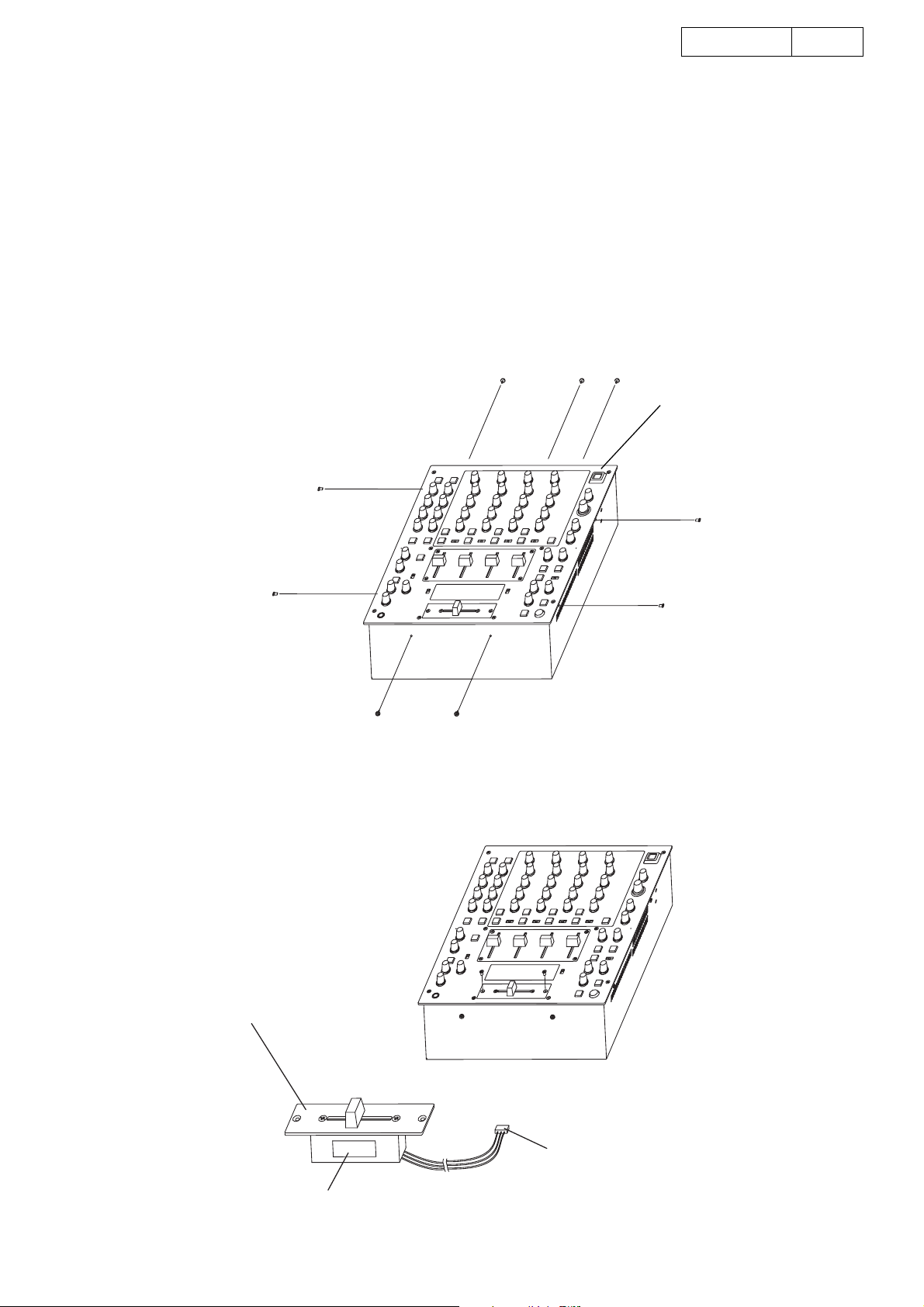
DISASSEMBLY
(Follow the procedure below in reverse order when reassembling.)
1. Top Panel Unit
(1)Remove 9 screws and pull up Top Panel Unit.
(2)Disconnect FFC cable and Connector.
(3)Detach Top Panel Unit.
Note:
Do not pull out aslsnt to prevent FFC cable damage.
●
●Do not fail to pull AC cord from wall outlet before
disconnect the FFC cable.
if AC cord is remained plugged into wall outlet,
power is kept supplied in the unit, which may cause
danger.
DN-X1500
Top Panel Unit
3
2. Cross Feder Unit
(1)Remove 2 screws and pull up Cross Feder Unit.
(2)Disconnect Connector.
Cross Feder Unit
Label face
Connector
3
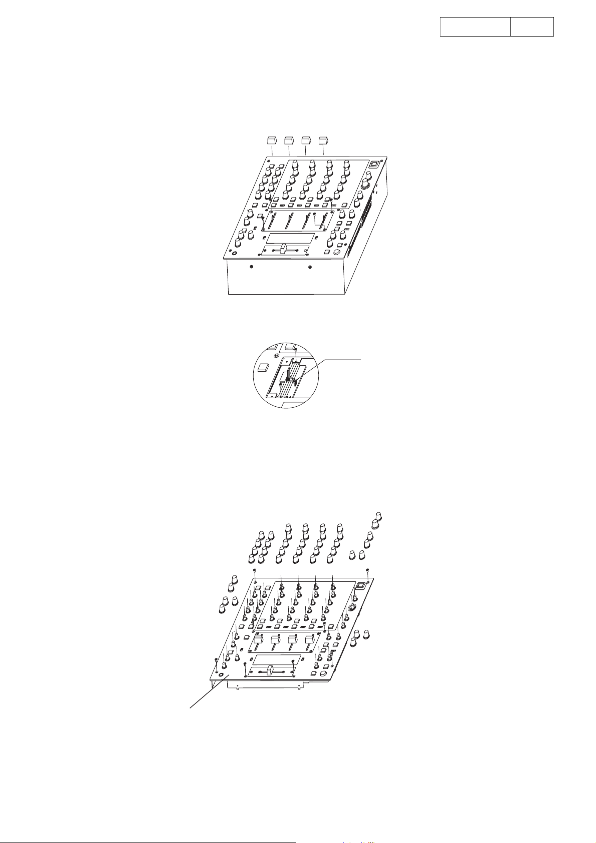
3. CH Fader Unit
(1)Remove 4 knobs.
(2)Remove 4 screws and pull up CH Fader Panel.
(3)Remove 2 screws for each CH.
(4)Disconnect Connector.
(5)Detach CH Fader Unit.
DN-X1500
4
4. Front Panel
(1)Pull out the knobs.
(2)Remove 8 screws.
(3)Pull up Front Panel.
5'0514.'8'4
Front Panel
4
DN-X1500
SERVICE MODE SPECIFICATION
*How the product performs when the operation buttons for μcom control are pressed (including control input) is described in
the table below.
1. POWER ON
Function Description Display Remarks
POWER
Service
Mode
2. CH GAIN VR
Function Description Display Remarks
CH LEVEL
METER
(1)Turns power ON/OFF.
(2)Switches power ON when OFF.
① Enters in the service mode when power on
while pressing MIC POST ON/OFF button and
E F F E C T L O O P O N / O F F b u t t o n .
② For canceling the service mode, turn power off/on.
(1) When you turn this VR, LED of CH level meter
is lit.
①Displays Service. ①Refer to CH GAIN VR.
②Refer to MASTER LEVEL VR.
③Refer to SAMPER ASSIGN.
④Refer to CROSSFADER ASSIGN.
① VR position is 0 : LED is not lit.
② VR position is 10 : All LED is lit.
5
3. MASTER LEVEL VR
Function Description Display Remarks
MASTER
LEVEL
METER
(1) When you turn this VR, LED of master level
meter is lit.
①VR position is 0 : LED is not lit.
② VR position is 10 : All LED is lit.
4. (SAMPLER) CROSSFADER ASSIGN switch
Function Description Display Remarks
FL mode
(1) You can select FL display mode.
① A : FL tube is not lit.
② B : All FL tube is lit.
③ POST : Displays VR checking or
LED checking.
5
DN-X1500
5. SAMPLER ASSIGN switch
Function Description Display Remarks
FADER VR
CHECK
OFF
CH1
CH2
CH3
CH4
MAIN
MIC
MASTER
(1)When CROSSFADER ASSIGN switch is set
to POST, you can check the fader VR and LED.
(1)When selected OFF, it becomes the LED off
modde.
(1)When selected CH1, it becomes the mode of
reading/displaying CH1 fader VR value.
(1)When selected CH2, it becomes the mode of
reading/displaying CH2 fader VR value.
(1)When selected CH3, it becomes the mode of
reading/displaying CH3 fader VR value.
(1)When selected CH4, it becomes the mode of
reading/displaying CH4 fader VR value.
(1)When selected MAIN MIC, it becomes the
LED on mode.
(1)When selected MASTER, it becomes the
mode of reading/displaying crossfader VR value.
①Displays LED OFF.
①Displays 0〜100.
②Fader position is 0 : 0
③Fader position is 10 :100
①Displays 0〜100.
②Fader position is 0 : 0
③Fader position is 10 : 100
①Displays 0〜100.
②Fader position is 0 : 0
③Fader position is 10 : 100
①Displays 0〜100.
②Fader position is 0 :0
③Fader position is 10 : 100
① Displays LED ON.
①Displays 0〜100.
②Fader position is Left side : 0
③Fader position is Right side : 100
①Refer to CROSSFAER ASSGIN.
6
6.
COM VERSION CHECK
μ
You can check the μcom version at "Preset Functions".
Please refer to the Instructions Manual.
6
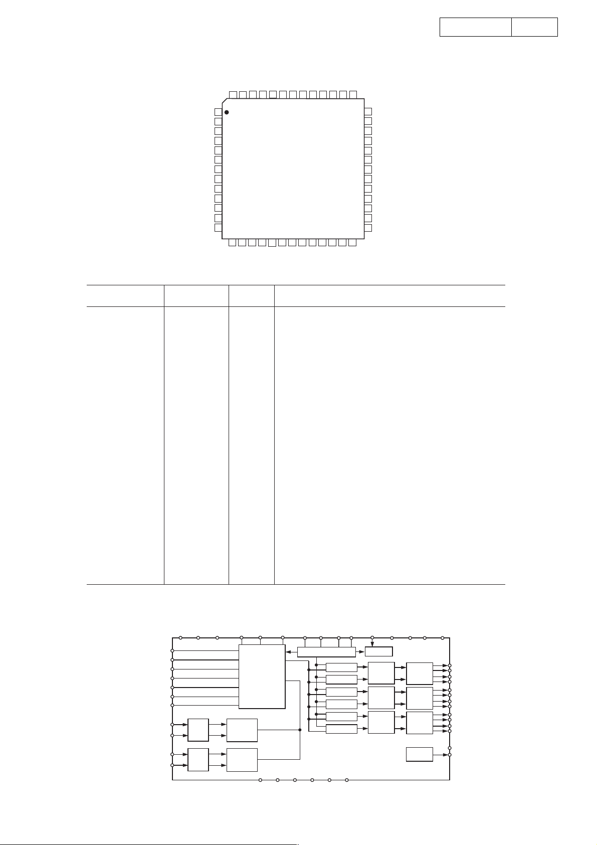
SEMICONDUCTORS
Only major semiconductors are shown, general semiconductors etc. are omitted to list.
IC's
●
Note: Abbreviation ahead of IC No. indicates the name of P.W.B., etc.
MN102H74D (IC101)
DN-X1500
7
75
76
100
1
51
50
26
25
MN102H74D Terminal Function
No. Pin Name Symbol I/O DET
1 P50,WAIT _WAIT I - - Pu H - HI R/W timing wait signal
2 P51,_RE _RD O - - Pu H - Read signal
3 P52,_WEL _WEL O - - Pu H - Write signal
4 P53,_WEH _DSP_REQ O - ON - Hi-z H System <-> DSP REQ signal
5 P60,_CS0 _CS0 O - - Pu H - Chip select signal 1st address of Flash ROM:
6 P61,_CS1 _CS_DSP O - - Pu H - Chip select of expansion port
7 P62,_CS2 _HBR O - - Pu H - DSP select signal Host Interface
8 P63,_CS3 _DSP_ACK I - ON - Hi-z - System <-> DSP ACK signal
9 P64,TM0IO,_BREQ _BREQ I - - Pu H 10 P65,TM1IO,_BRACK _BRACK O - Pu H - When bus open, 'L' output.
11 P66,_W R _DAC_RST O - ON - H H Reset of ADC, DAC, and DIT
12 _W ORD _WORD I - - L L - Select width of data bit bus 'L': 16bit
13 P20,A00 A00 A/O - ON - Hi-z - Address bus
14 P21,A01 A01 A/O - ON - Hi-z - Address bus
15 P22,A02 A02 A/O - ON - Hi-z - Address bus
16 P23,A03 A03 A/O - ON - Hi-z - Address bus
17 Vdd Vdd - - - - - - Power supply(+3.3V)
18 P54,BOSC,SYSCLK RESERVE1 O - ON - L H Signal for test
19 Vss Vss - - - - - - GND(0V)
20 XI XI - - - - - - Not used
21 XO XO - - - - - - Not used
22 Vdd Vdd - - - - - - Power supply(+3.3V)
23 OSCI OSCI I - - - - - This Need 12MHz for USB communication
24 OSCO OSCO O - - - - - Output OSCI
25 MODE MODE I - - H H 26 P24,A04 A04 A/O - ON - Hi-z - Address bus
27 P25,A05 A05 A/O - ON - Hi-z - Address bus
28 P26,A06 A06 A/O - ON - Hi-z - Address bus
29 P27,A07 A07 A/O - ON - Hi-z - Address bus
30 P30,A08 A08 A/O - ON - Hi-z - Address bus
31 P31,A09 A09 A/O - ON - Hi-z - Address bus
32 P32,A10 A10 A/O - ON - Hi-z - Address bus
33 P33,A11 A11 A/O - ON - Hi-z - Address bus
34 Vdd Vdd - - - - - - Power supply(+3.3V)
35 P34,A12 A12 A/O - ON - Hi-z - Address bus
36 P35,A13 A13 A/O - ON - Hi-z - Address bus
37 P36,A14 A14 A/O - ON - Hi-z - Address bus
38 P37,A15 A15 A/O - ON - Hi-z - Address bus
Internal Pull Up is 10〜90 ( KΩ ), Ave : 30 ( KΩ )
※
Int
PU Ext Res Ini Function
Panel ucom control: When DSP boot, system bus
open. 'L': open
Mode set
'H': Memory expansion/single chip mode
7
DN-X1500
C
C
Ω
8
No. Pin Name Symbol I/O DET
39 P40,A16 A16 A/O - ON - Hi-z - Address bus
40 P41,A17 A17 A/O - ON - Hi-z - Address bus
41 P42,A18 A18 A/O - ON - Hi-z - Address bus
42 P43,(TM2IO),A19 A19 A/O - - Pu H 43 Vss Vss - - - - - - GND(0V)
44 P44,(TM3IO),A20 _CDDEC_L
45 P45,(TM4IO),A21 _CDDEC_L
46 P46,(TM5IO),A22 _DAC_CS O - ON - Hi-z H DAC chip select 'L': available
47 P47,_CS0S,(TM6IO),A23 _DIT_CS O - - Pd L H
48 P70,_CS1S,(TM7IO),SBI3 DIT_DIN I - ON - Hi-z H DIT data input
49 P71,_CS2S,(TM8IO),SBO3 CLOCK_A O - - Pd L L
50 P72,_CS3S,(TM9IO),SBT3 DATA_A O - ON - Hi-z L
51 P80,TM10IOA,WDOUT PLGIN_L I - - Pu H H
52 P81,TM10IOB,STOP PLGIN_R I - - Pu H H
53 USBMODE USBMODE - - - - - - USB mode selectable terminal, connect to GND
54 Vdd Vdd - - - - - - Power supply(+3.3V)
55 D+ D+ - - - Pu - -
56 D- D- - - - - - 57 Vss Vss - - - - - - GND(0V)
58 P82,SBI2 RxD I - - Pu H - 75000bps Need to convert level
59 P83,SBO2,TM11IOA TxD O - - Pu H H 75000bps Need to convert level
60 P84,SBT2,TM11IOB _MONO I - ON - Hi-z - MONO/STEREO SW 'L': MONO
61 Vss Vss - - - - - - GND(0V)
62 P90,AN0,TM12IOA ATT I Ad - - - - Adjust VR for Master output (BAL/UNBAL)
63 P91,AN1,TM12IOB _STB_CLR O - - Pd L L
64 P92,AN2,TM13IOA CLOCK_B O - - Pd L L
65 P93,AN3,TM13IOB DATA_B O - ON - Hi-z L Electric VR(TC94A32)/SelectorTC9162 data signal
66 Vdd Vdd - - - - - - Power supply(+3.3V)
67 PA0,SBI1,AN4 _FPLAY1 O - - Pu H H Ch1 Fader PLAY output 20msec 'L' pulse
68 PA1,SBO1,AN5,SDA1 _FCUE1 O - - Pu H H Ch1 Fader CUE output 20msec 'L' pulse
69 PA2,SBT1,AN6,SCL1 _FPLAY2 O - - Pu H H Ch2 Fader PLAY output 20msec 'L' pulse
70 PA3,SBI0,AN7 _FCUE2 O - - Pu H H Ch2 Fader CUE output 20msec 'L' pulse
71 PA4,SBO0,SDA0 _FPLAY3 O - - Pu H H Ch3 Fader PLAY output 20msec 'L' pulse
72 PA5,SBT0,SCL0 _FCUE3 O - - Pu H H Ch3 Fader CUE output 20msec 'L' pulse
73 TEST1 SBD4 I - - Pu - -
74 TEST2 SBT4 I - - Pu - 75 _NMI _NMI I Lv - - H H
76 PB0,_IRQ0 _DSP_BPM I Ed ON - - Trigger terminal for BPM counter by DSP
77 PB1,_IRQ1 DSP_COM O - - Pu H - System <-> DSP REQ2 signal
78 PB2,_IRQ2 RESERVE4 I - - Pu H - Signal for test
79 PB3,_IRQ3 MUTE O - - Pu H H Analog/Digital mute 'H': Mute ON
80 PB4,_IRQ4 _FPLAY4 O - - Pu H H Ch4 Fader PLAY output 20msec 'L' pulse
81 PB5,_IRQ5 _FCUE4 O - - Pu H H Ch4 Fader CUE output 20msec 'L' pulse
82 _RST _RESET I Lv - - L - Reset signal 'L': Reset
83 Vdd Vdd - - - - - - Power supply(+3.3V)
84 P00,D00 D00 D/O - ON - Hi-Z - Data bus
85 P01,D01 D01 D/O - ON - Hi-Z - Data bus
86 P02,D02 D02 D/O - ON - Hi-Z - Data bus
87 P03,D03 D03 D/O - ON - Hi-Z - Data bus
88 P04,D04 D04 D/O - ON - Hi-Z - Data bus
89 P05,D05 D05 D/O - ON - Hi-Z - Data bus
90 P06,D06 D06 D/O - ON - Hi-Z - Data bus
91 P07,D07 D07 D/O - ON - Hi-Z - Data bus
92 Vss Vss - - - - - - GND(0V)
93 P010,D08,(TM2IO) D08 D/O - ON - Hi-Z - Data bus
94 P011,D09,(TM3IO) D09 D/O - ON - Hi-Z - Data bus
95 P012,D10,(TM4IO) D10 D/O - ON - Hi-Z - Data bus
96 P013,D11,(TM5IO) D11 D/O - ON - Hi-Z - Data bus
97 P014,D12,(TM6IO) D12 D/O - ON - Hi-Z - Data bus
98 P015,D13,(TM7IO) D13 D/O - ON - Hi-Z - Data bus
99 P016,D14,(TM8IO) D14 D/O - ON - Hi-Z - Data bus
100 P017,D15,(TM9IO) D15 D/O - ON - Hi-Z - Data bus
O - ON - Hi-z H Latch to codec1 'L': available
O - ON - Hi-z H Latch to codec2 'L': available
Int
PU Ext Res Ini Function
Address bus
Need pull up to extension for DSP boot control
DIT chip select
'L': available (be pull down in DSP)
CODEC(AD1838A)/DAC(PCM1791A)/DIT(AK4103)
data output clock signal
CODEC(AD1838A)/DAC(PCM1791A)/DIT(AK4103)
data signal
Lch SEND/RETURN connection status
'H': connect
Rch SEND/RETURN connection status
'H': connect
Connect USB terminal D+. 24
connected in series.
Connect USB terminal D-. 24Ω resistance is
connected in series.
TC94A32/TC9162 ALL STB set to L
'L': L set , CODEC reset
Electric VR(TC94A32)/SelectorTC9162 data output
clock signal
10kΩ Connection output for
Pull up 4.7kΩ
onboard write of internal form.
Pull up 4.7kΩ
onboard write of internal form.
〜
〜 10kΩ Connection output for
resistance is
8
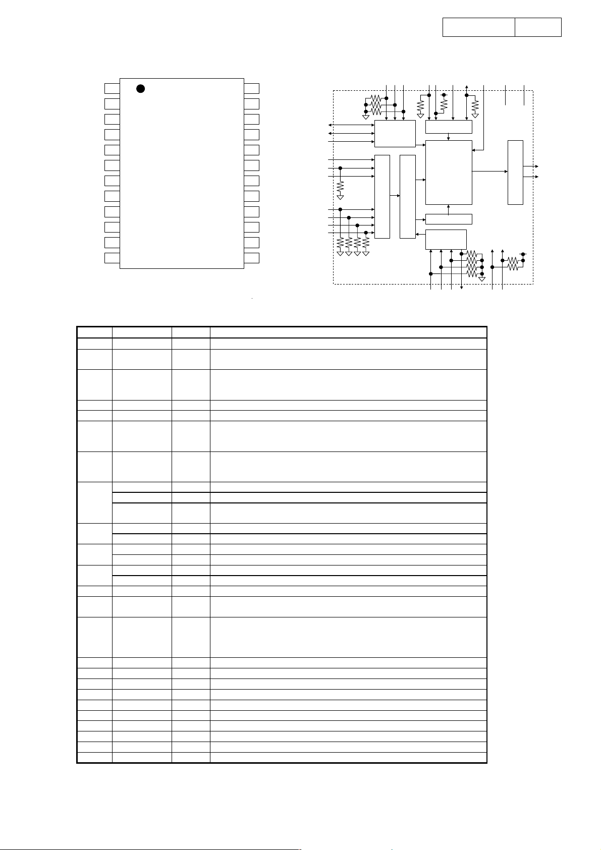
TMP86CM47U (IC301)
DN-X1500
9
33
34
23
22
TOP VIEW
44
1
TMP86CM47U Terminal Function
11
Pin No. Pin Name Symbol I/O DET Ext Res Ini Function
VSS VSS
1
2
XIN XIN
XOUT XOUT
3
4
TEST TEST
VDD VDD
5
6
P21 ADR1
P22 ADR2
7
8
RESET_ RESET_
P20 DSPBSY
9
10
P00 ADR3
P01 ADR4
11
12
RXD RXD
TXD TXD
13
14
SO FLSD
P05 FLCS
15
16
SCK FLCLK
P07 TEST1
17
18
P17 FLRST
P16 DRST
19
20
P15 BREQ
P14 LDLCH
21
22
P13 LDCLK
P12 LDDAT1
23
P11 LDDAT2
24
P10 LDDAT3
25
AIN0 KEYIN0
26
AIN1 KEYIN1
27
AIN2 KEYIN2
28
AIN3 KEYIN3
29
AIN4 KEYIN4
30
AIN5 KEYIN5
31
AIN6 KEYIN6
32
33
AIN7 KEYIN7
VAREF VARFF
34
35
AVDD AVDD
AVSS AVSS
36
37
P40 KEYIN8
P41 KEYIN9
38
39
P42 KEYIN10
P43 KEYIN11
40
41
P44 KEYIN12
P45 KEYIN13
42
43
P46 KEYIN14
P47 KEYIN15
44
-----
-----
-----
-----
----O-Pu-H
O-Pu-H
-----
I-PuHO-Pu-H
O-Pu-H
I--HO-PuHH
O-PuHH
O-PuHH
O-PuHH
O- --H
O-PdLL
O-PdLL
O-PuHH
O-PuHH
O-Pu-H
O-Pd-L
O-Pd-L
O- LLL
I----
I----
I----
I----
I----
I----
I----
I----
-----
-----
-----
I-Pu-H
I-Pu-H
I-Pu-H
I-Pu-H
I-Pu-H
I-Pu-H
I-Pu-H
I-Pu-H
GND (0V)
Oscillation input 16MHz
Oscillation output
Fixed to GND
Power (+5.0V)
Address decode signal 1
Address decode signal 2
Reset input
Boot flag (L: during boot)
Address decode signal 3
Address decode signal 4
Serial receive signal
Serial send signal
M66005AFP-SDATA
M66005AFP-CA
M66005AFP-CLK
Not used
M66005AFP reset signal (L: Reset)
DSP reset (L: Reset)
System ucom stop signal
LED driver latch signal
Clock for LED driver data sending
LED driver data 1
LED driver data 2
LED driver data 3
Key input 0 (Volume)
Key input 1 (Volume)
Key input 2 (Volume)
Key input 3 (Volume)
Key input 4 (Volume)
Key input 5 (Volume)
Key input 6 (Volume)
Key input 7 (Volume)
Power (+5.0V), Analog ref.V for A/D conversion
Power (+5.0V)
GND (0V), Analog GND for A/D conversion
Key input 8 (Key matrix)
Key input 9 (Key matrix)
Key input 10 (Key matrix)
Key input 11 (Key matrix)
Key input 12 (Key matrix)
Key input 13 (Key matrix)
Key input 14 (Key matrix)
Key input 15 (Key matrix)
12
9
DN-X1500
ADSST-MEL100 (DSP:IC101)
10
12
14
11
13
15
TOP VIEW
BOTTOM VIEW
ADSST-MEL100 Terminal Function
No. No. No.No. No.
A1
A2
A3
A4
A5
A6
A7
A8
A9
A10
A11
A12
A13
A14
A15
No. No. No. No.
F1
F2
F3
F4
F5
F6
F7
F8
F9
F10
F11
F12
F13
F14
F15
No. No. No. No. No.
L1
L2
L3
L4
L5
L6
L7
L8
L9
L10
L11
L12
L13
L14
L15
Pin Name Pin Name Pin Name Pin Name Pin Name
NC
BMSTR
BMS_
SPIDS_
EBOOT
LBOOT
SCLK2
D3B
L0DAT[4]
L0ACK
L0DAT[2]
L1DAT[6]
L1CLK
L1DAT[2]
NC
B1
B2
B3
B4
B5
B6
B7
B8
B9
B10
B11
B12
B13
B14
B15
TRST_
TDI
RPBA
MOSI
FS0
SCLK1
D2B
D3A
L0DAT[7]
L0CLK
L0DAT[1]
L1DAT[4]
L1ACK
L1DAT[0]
RSTOUT_
C1
C2
C3
C4
C5
C6
C7
C8
C9
C10
C11
C12
C13
C14
C15
TMS
EMU_
GND
SPICLK
D0B
D1A
D2A
FS2
FS3
L0DAT[6]
L1DAT[7]
L1DAT[3]
L1DAT[1]
DATA[45]
DATA[47]
D1
D2
D3
D4
D5
D6
D7
D8
D9
D10
D11
D12
D13
D14
D15
TD0
TCK
FLAG11
MISO
SCLK0
D1B
FS1
VDDINT
SCLK3
L0DAT[5]
L0DAT[3]
L1DAT[5]
DATA[42]
DATA[46]
DATA[44]
Pin Name Pin Name Pin Name Pin Name Pin Name
FLAG5
FLAG7
FLAG9
FLAG6
VDDINT
GND
GND
GND
GND
GND
VDDINT
DATA[37]
DATA[40]
DATA[38]
DATA[36]
G1
G2
G3
G4
G5
G6
G7
G8
G9
G10
G11
G12
G13
G14
G15
FLAG1
FLAG2
FLAG4
FLAG3
VDDEXT
GND
GND
GND
GND
GND
VDDEXT
DATA[34]
DATA[35]
DATA[33]
DATA[32]
H1
H2
H3
H4
H5
H6
H7
H8
H9
H10
H11
H12
H13
H14
H15
FLAG0
IRQ0_
VDDINT
IRQ1_
VDDINT
GND
GND
GND
GND
GND
VDDINT
DATA[29]
DATA[28]
DATA[30]
DATA[31]
J1
J2
J3
J4
J5
J6
J7
J8
J9
J10
J11
J12
J13
J14
J15
IRQ2_
ID1
ID2
ID0
VDDEXT
GND
GND
GND
GND
GND
VDDEXT
DATA[26]
DATA[24]
DATA[25]
DATA[27]
Pin Name Pin Name Pin Name Pin Name Pin Name
ADDR[19]
ADDR[17]
ADDR[21]
ADDR[2]
VDDEXT
VDDINT
VDDEXT
VDDINT
VDDEXT
VDDINT
VDDEXT
CAS_
DATA[20]
DATA[16]
DATA[18]
M1
M2
M3
M4
M5
M6
M7
M8
M9
M10
M11
M12
M13
M14
M15
ADDR[16]
ADDR[12]
ADDR[18]
ADDR[6]
ADDR[0]
MS1
BR6
VDDEXT
WR
SDA10
RAS_
ACK
DATA[17]
DMAG2
DMAG1
N1
N2
N3
N4
N5
N6
N7
N8
N9
N10
N11
N12
N13
N14
N15
ADDR[14]
ADDR[15]
ADDR[10]
ADDR[5]
ADDR[1]
MS0
BR5
BR2
BRST
SDCKE
CS_
CLK_CFG1
CLK_CFG0
AVDD
DMAR1
P1
P2
P3
P4
P5
P6
P7
P8
P9
P10
P11
P12
P13
P14
P15
ADDR[13]
ADDR[9]
ADDR[8]
ADDR[4]
MS2
SBTS_
BR4
BR1
SDCLK1
SDCLK0
REDY
CLKIN
DQM
AVSS
DMAR2
123456789
A
B
C
D
E
F
G
H
J
K
L
M
N
P
R
E1
E2
E3
E4
E5
E6
E7
E8
E9
E10
E11
E12
E13
E14
E15
No.
K1
K2
K3
K4
K5
K6
K7
K8
K9
K10
K11
K12
K13
K14
K15
R1
R2
R3
R4
R5
R6
R7
R8
R9
R10
R11
R12
R13
R14
R15
10
FLAG10
RESET_
FLAG8
D0A
VDDEXT
VDDINT
VDDEXT
VDDINT
VDDEXT
VDDINT
VDDEXT
L0DAT[0]
DATA[39]
DATA[43]
DATA[41]
TIMEXP
ADDR[22]
ADDR[20]
ADDR[23]
VDDINT
GND
GND
GND
GND
GND
VDDINT
DATA[22]
DATA[19]
DATA[21]
DATA[23]
NC
ADDR[11]
ADDR[7]
ADDR[3]
MS3
PA
BR3
RD
CLKOUT
HBR
HBG
CLKDBL
XTAL
SDWE_
NC
10
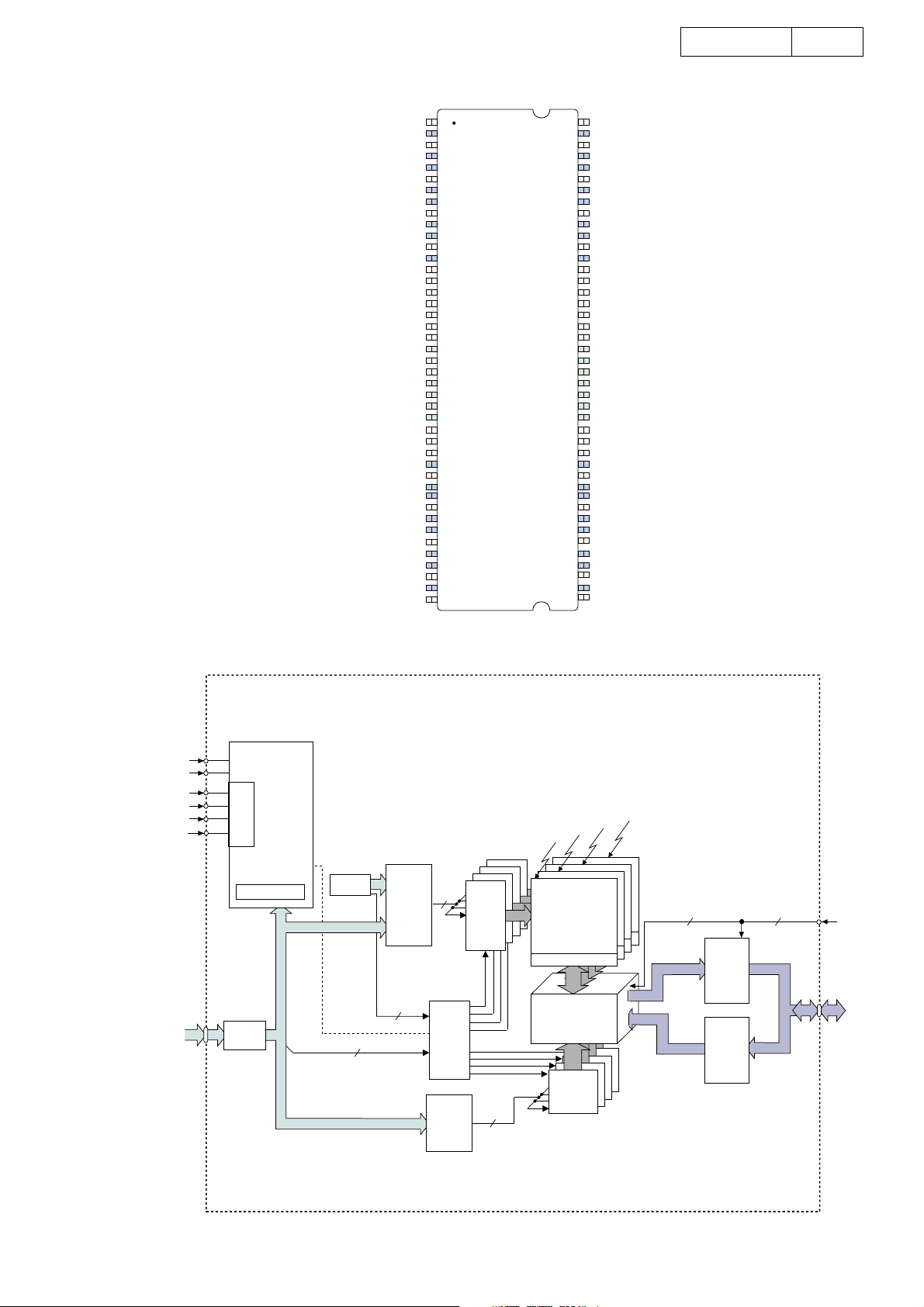
128M-SDRAM (DSP:IC102)
DN-X1500
11
V
DQ0
V
DD
DQ1
DQ2
V
SS
DQ3
DQ4
V
DD
DQ5
DQ6
V
SS
DQ7
NC
V
DQM0
WE#
CAS#
RAS#
CS#
A11
BA0
BA1
A10
A0
A1
A2
DQM2
V
NC
DQ16
SS
V
DQ17
DQ18
V
DD
DQ19
DQ20
V
SS
DQ21
DQ22
DD
V
DQ23
V
DD
1
2
3
Q
4
5
6
Q
7
8
9
Q
10
11
12
Q
13
14
15
DD
16
17
18
19
20
21
22
23
24
25
26
27
28
29
DD
30
31
32
Q
33
34
35
Q
36
37
38
Q
39
40
41
Q
42
43
DD
86
V
SS
85
DQ15
84
SS
Q
V
83
DQ14
82
DQ13
81
V
DD
DQ12
DQ11
V
SS
Q
DQ10
DQ9
V
DD
DQ8
NC
V
SS
DQM1
NC
NC
CLK
CKE
A9
A8
A7
A6
A5
A4
A3
DQM3
V
SS
NC
DQ31
DD
V
DQ30
DQ29
V
SS
Q
DQ28
DQ27
V
DD
DQ26
DQ25
SS
Q
V
DQ24
SS
V
Q
Q
Q
Q
80
79
78
77
76
75
74
73
72
71
70
69
68
67
66
65
64
63
62
61
60
59
58
57
56
55
54
53
52
51
50
49
48
47
46
45
44
Block Diagram
CKE
CLK
CS#
WE#
CAS#
RAS#
A0–A11,
BA0, BA1
14
DECODE
COMMAND
MODE REGISTER
ADDRESS
REGISTER
CONTROL
LOGIC
12
Note: The # symbol indicates signal is active LOW.
BANK0
REFRESH
12
COUNTER
12
8
ROW-
ADDRESS
MUX
2
2
12
BANK
CONTROL
LOGIC
COLUMNADDRESS
COUNTER/
LATCH
BANK0
ROW-
ADDRESS
LATCH
&
DECODER
4096
8
MEMORY
(4,096 x 256 x 32)
SENSE AMPLIFIERS
I/O GATING
DQM MASK LOGIC
READ DATA LATCH
WRITE DRIVERS
COLUMN
DECODER
BANK1
BANK0
ARRAY
8192
256
(x32)
BANK2
BANK3
4
DATA
OUTPUT
32
REGISTER
DATA
INPUT
32
REGISTER
4
32
DQM0–
DQM3
DQ0–
DQ31
11
128M-SDRAM Terminal Function
Pin NO. Symbol Type Description
68 CLK I Clock
67 CKE I Clock Enable
20 CS# I Chip Select
17, 18, 19 WE#, CAS#, RAS# I Command Inputs
16, 71, 28, 59 DQM0-DQM3 I Input/Outout Mask
22, 23 BA0, BA1 I Bank Address Input(s)
21, 24-27, 60-66 A0-A11 I Address Inputs
2, 4, 5, 7, 8, 10, 11, 13, 31, 33, 34, 36, 37, 39,
40, 42, 45, 47, 48, 50, 51, 53, 54, 56, 74, 76,
77, 79, 80, 82, 83, 85
14, 30, 57, 69, 70, 73 NC - No Connect
3, 9, 35, 41, 49, 55, 75, 81 V
6, 12, 32, 38, 46, 52, 78, 84 V
1, 15, 29, 43 V
44, 58, 72, 86 V
DQ0-DQ31 I/O Data I/Os
DD
Q Supply DQ Power Supply
SSQ Supply DQ Ground
DD
SS
Supply Power Supply: +3.3V ±0.3V
Supply Ground
DN-X1500
12
12
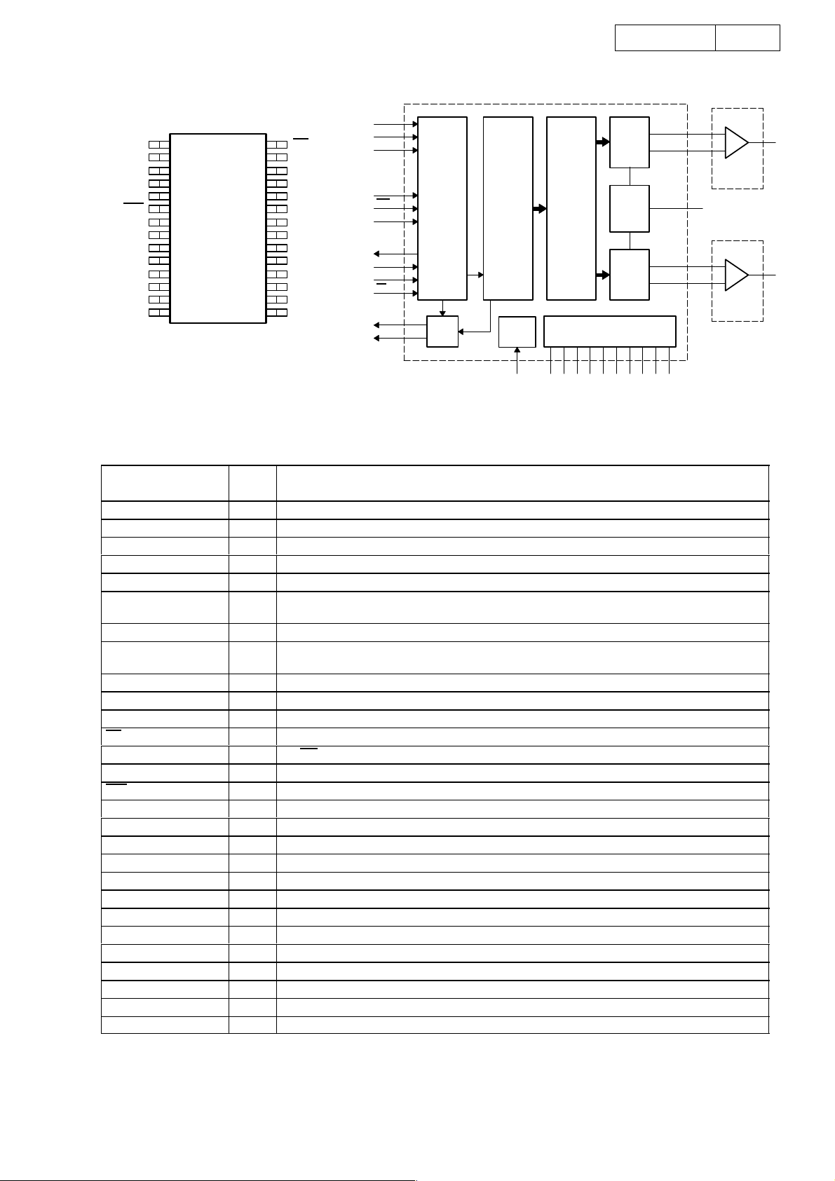
AD1838A (IC401,501)
∆
∆
DN-X1500
13
DSDATA2
DSDATA1
AGND
OUTLN3
DGND
OUTLP3
DVDD
39
38
DBCLK
37
DLRCLK
DAUXDATA
36
35
M/S
34
AGND
33
N/C
32
N/C
31
N/C
30
AGND
29
AVDD
28
OUTRP3
OUTRN3
27
DVDD
CLATCH
CIN
PD/RST
AGND
OUTLN1
OUTLP1
OUTRN1
OUTRP1
AGND
AVDD
OUTLN2
OUTLP2
DGND
CCLK
COUT
ASDATA
ODVDD
MCLK
ALRCLK
ABCLK
ADCLN
)
ADCLP
ADCRN
AAUXDATA3
50 494847 46 45 44 43 42 41 40
51
52
1
2
3
4
5
6
7
8
9
10
11
12
13
14 15 16 17 18 19 20 21 22 23 24 25 26
OUTRP2
OUTRN2
AGND
FILTD
AD1838A
TOP VIEW
(Not to Scale
FILTR
AVDD
DSDATA3
ADCRP
PIN FUNCTION DESCRIPTIONS
Input/
Pin No. Mnemonic Output Description
1, 39 DVDD Digital Power Supply. Connect to digital 5 V supply.
2 CLATCH I Latch Input for Control Data.
3 CIN I Serial Control Input.
4 PD/RST I Power-Down/Reset.
5, 10, 16, 24, 30, 34 AGND Analog Ground.
6, 12, 25 OUTLNx O DACx Left Channel Negative Output.
7, 13, 26 OUTLPx O DACx Left Channel Positive Output.
8, 14, 27 OUTRNx O DACx Right Channel Negative Output.
9, 15, 28 OUTRPx O DACx Right Channel Positive Output.
11, 19, 29 AVDD Analog Power Supply. Connect to analog 5 V supply.
17 FILTD Filter Capacitor Connection. Recommended 10 µF/100 nF.
18 FILTR Reference Filter Capacitor Connection. Recommended 10 µF/100 nF.
20 ADCLN I ADC Left Channel Negative Input.
21 ADCLP I ADC Left Channel Positive Input.
22 ADCRN I ADC Right Channel Negative Input.
23 ADCRP I ADC Right Channel Positive Input.
31–33 N/C Not Connected.
35 M/S I ADC Master/Slave Select.
36 DAUXDATA O Auxiliary DAC Output Data.
37 DLRCLK I/O DAC LR Clock.
38 DBCLK I/O DAC Bit Clock.
40, 52 DGND Digital Ground.
41–43 DSDATAx I DACx Input Data (Left and Right Channels).
44 AAUXDATA3 I Auxiliary ADC3 Digital Input.
45 ABCLK I/O ADC Bit Clock.
46 ALRCLK I/O ADC LR Clock.
47 MCLK I Master Clock Input.
48 ODVDD Digital Output Driver Power Supply.
49 ASDATA O ADC Serial Data Output.
50 COUT O Output for Control Data.
51 CCLK I Control Clock Input for Control Data.
AAUXDATA3
DLRCLK
DBCLK
DSDATA1
DSDATA2
DSDATA3
DAUXDATA
ADCLP
ADCLN
ADCRP
ADCRN
DVDD
⌺−∆
ADC
⌺−∆
ADC
FUNCTIONAL BLOCK DIAGRAM
CINCLATCHCCLK COUT
CONTROL PORT
VOLUME
VOLUME
VOLUME
VOLUME
VOLUME
VOLUME
AD1838A
AGND AGNDAGNDAGNDDGNDDGND
DIGITAL
FILTER
DIGITAL
FILTER
SERIAL DATA
I/O PORT
13
MCLKASDATAABCLKALRCLKODVDDDVDD
CLOCK
DIGITAL
FILTER
DIGITAL
FILTER
DIGITAL
FILTER
PD/RST M/S
⌺-⌬
DAC
⌺-⌬
DAC
⌺-⌬
DAC
V
AVDD
REF
AVDD
OUTLP1
OUTLN1
OUTRP1
OUTRN1
OUTLP2
OUTLN2
OUTRP2
OUTRN2
OUTLP3
OUTLN3
OUTRP3
OUTRN3
FILTD
FILTR
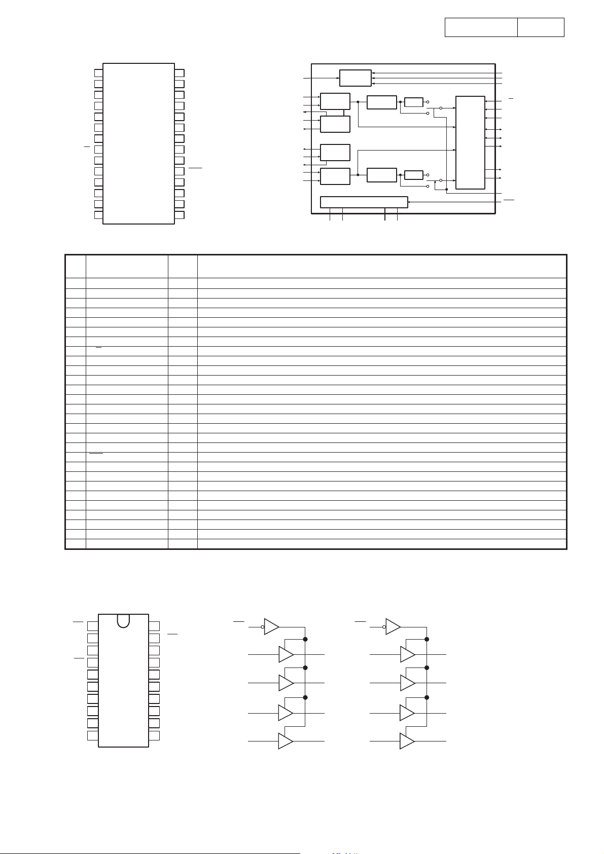
AK4103A (IC502)
Host Serial
Interface
Audio Serial
Interface
BICK
LRCK
TXP
MUX
CRCC Generator
Prescaler
RS422 Line Driver
Biphase
Encoder
DIF2
DIF1
DIF0
CKS1
CKS0
MCLK
BLS
TRANS
VSS
VDD
TXN
C1
U1
V1
FS0
FS1
FS2
FS3
Register
K
I
O
Block Diagram
DN-X1500
14
TRANS
PDN
MCLK
SDTI
BICK
LRCK 7
FS0/CSN 8
FS2/CCLK
FS3/CDTO 11
C1 12
1V1
2
3
4
5
6
9FS1/CDTI
10
Top
View
U1
24
23
DIF2
DIF1
22
DIF0
21
TXP
20
TXN
19
18
VSS
17
VDD
16
CKS1
15
CKS0
14
BLS
13
ANS
SDTI
CSN
CCL
CDT
CDT
ANS
PDN
AK4103A PIN/FUNCTION
No. Pin Name I/O Description
1 V1 I Validity Bit Input Pin
2 TRANS I Audio Routing Mode (Transparent Mode) Pin at Synchronous mode
0: Normal mode, 1: Audio routing mode (transparent mode)
3 PDN I Power Down & Reset Pin (Pull-up Pin)
When “L”, the AK4103A is powered-down, TXP/N pins are “L” and the
control registers are reset to default values.
4 MCLK I Master Clock Input Pin
5 SDTI I Audio Serial Data Input Pin
6 BICK I/O Audio Serial Data Clock Input/Output Pin
Serial Clock for SDTI pin which can be configured as an output based on
the DIF2-0 inputs.
7 LRCK I/O Input/Output Channel Clock Pin
Indicates left or right channel, and can be configured as an output based on
the DIF2-0 inputs.
FS0 I Sampling Frequency Select 0 Pin at Synchronous mode (Pull-down Pin)
8
CSN I Host Interface Chip Select Pin at Asynchronous mode (Pull-down Pin)
AKMODE I AK4112B Mode Pin at Audio routing mode (Pull-down Pin)
0: Non-AKM receivers mode, 1: AK4112B mode
FS1 I Sampling Frequency Select 1 Pin at Synchronous mode (Pull-down Pin)9
CDTI I Host Interface Data Input Pin at Asynchronous mode (Pull-down Pin)
FS2 I Sampling Frequency Select 2 Pin at Synchronous mode (Pull-down Pin)10
CCLK I Host Interface Bit Clock Input Pin at Asynchronous mode (Pull-down Pin)
FS3 I Sampling Frequency Select 3 Pin at Synchronous mode (Pull-down Pin)11
CDTO O Host Interface Data Output Pin at Asynchronous mode (Pull-down Pin)
12 C1 I Channel Status Bit Input Pin
13 ANS I Asynchronous/Synchronous Mode Select Pin (Pull-up Pin)
14 BLS I/O Block Start Input/Output Pin (Pull-down Pin)
0: Asynchronous mode, 1: Synchronous mode
In normal mode, the channel status block output is “H” for the first four
bytes. In audio routing mode, the pin is configured as an input. When PDN
pin = “L”, BLS pin goes “H” at Normal mode.
15 CKS0 I Clock Mode Select 0 Pin (Pull-up Pin)
16 CKS1 I Clock Mode Select 1 Pin (Pull-down Pin)
17 VDD 18 VSS - Ground Pin, 0V
19 TXN O Negative Differential Output Pin
20 TXP O Positive Differential Output Pin
21 DIF0 I Audio Serial Interface Select 0 Pin (Pull-down Pin)
22 DIF1 I Audio Serial Interface Select 1 Pin (Pull-down Pin)
23 DIF2 I Audio Serial Interface Select 2 Pin (Pull-down Pin)
24 U1 I User Data Bit Input Pin for Channel 1 (Pull-down Pin)
Notes:
1. Internal pull-up and pull-down resistors are connected on-chip. The value of the resistors is 43kΩ (typ).
Power Supply Pin, 4.75V∼5.25V
2. All input pins except internal pull-down/pull-up pins should not be left floating.
14
PCM1791A (IC402)
FUNCTIONAL BLOCK DIAGRAM
Power Supply
RST
SCK
Advanced
Segment
DAC
Modulator
V
OUT
L+
V
OUT
L–
Bias
and
Vref
V
CC
F
V
DD
AGNDR
V
CC
R
AGNDL
AGNDF
D/S and Filter
8
Oversampling
Digital
Filter
and
Function
Control
Audio
Data Input
I/F
LRCK
BCK
DATA
MDO
MDI
MC
MS
AGNDC
V
CC
C
DGND
Current
Segment
DAC
and
I/V Buffer
V
COM
Function
Control
I/F
Zero
Detect
ZEROL
ZEROR
System
Clock
Manager
MSEL
MUTE
V
CC
L
V
OUT
R–
V
OUT
R+
D/S and Filter
Current
Segment
DAC
and
I/V Buffer
(TOP VIEW)
DD
R–
1
2
3
4
5
6
7
8
9
R
10
11
12
13
14
LRCK
BCK
DATA
MUTE
SCK
RST
V
DGND
AGNDF
V
CC
AGNDR
V
OUT
V
OUT
V
COM
R+
DN-X1500
28
27
26
25
24
23
22
21
20
19
18
17
16
15
MS
MC
MDI
MDO
MSEL
ZEROL
ZEROR
V
F
CC
V
L
CC
AGNDL
V
OUT
V
OUT
AGNDC
C
V
CC
L–
L+
15
TERMINAL
NAME PIN
AGNDC 16 – Analog ground (internal bias and current DAC)
AGNDF 9 – Analog ground (DACFF)
AGNDL 19 – Analog ground (L-channel I/V)
AGNDR 11 – Analog ground (R-channel I/V)
BCK 2 I Bit clock input. Connected to GND for DSD mode
DATA 3 I Serial audio data input for normal operation. L-channel audio data input for external DF and DSD
DGND 8 – Digital ground
LRCK 1 I Left and right clock (fS) input for normal operation. WDCK clock input in external DF mode.
MC 27 I Shift clock for function control register
MDI 26 I/O Serial data input for function control register
MDO 25 O Serial data output for function control register
MS 28 I/O Mode control chip select and latch signal
MSEL 24 I I2C/SPI select
MUTE 4 I Analog output mute control for normal operation. R-channel audio data input for external DF mode
RST 6 I Reset
SCK 5 I System clock input. BCK (64 fS) clock input for DSD mode
VCCC 15 – Analog power supply (internal bias and current DAC), 5 V
VCCF 21 – Analog power supply (DACFF), 5 V
VCCL 20 – Analog power supply (L-channel I/V), 5 V
VCCR 10 – Analog power supply (R-channel I/V), 5 V
V
COM
V
DD
V
L+ 17 O L-channel analog voltage output +
OUT
V
V
V
ZEROL 23 O Zero flag for L-channel
ZEROR 22 O Zero flag for R-channel
(1)
(2)
(3)
(4)
L– 18 O L-channel analog voltage output –
OUT
R+ 13 O R-channel analog voltage output +
OUT
R– 12 O R-channel analog voltage output –
OUT
Schmitt-trigger input, 5-V tolerant
Schmitt-trigger input and output. 5-V tolerant input. In I2C mode, this pin becomes an open-drain 3-state output; otherwise, this pin is a CMOS
output.
3-state output
Schmitt-trigger input and output. 5-V tolerant input and CMOS output
Terminal Functions
I/O
(1)
modes
R-channel audio data for DSD mode
(1)
(1)
14 – Internal bias decoupling pin
7 – Digital power supply, 3.3 V
DESCRIPTIONS
(1)
(1)
(1)
(2)
(3)
(4)
(1)
(1)
15
PCM1804 (IC301,305,309,313)
DN-X1500
16
V
REF
AGNDL
COM
V
IN
V
IN
V
FMT0
FMT1
S/M
OSR0
OSR1
OSR2
BYPAS
DGND
V
L
2
3
L
4
L+
5
L
-
6
7
TOP VIEW
8
9
10
11
12
13
14
DD
28
V
REF
R
27
AGNDR
26
COM
V
25
IN
R+
V
24
IN
R
V
-
23
AGND
22
V
CC
21
OVFL
20
OVFR
19
RST
18
SCKI
17
LRCK/DSDBCK
16
BCK/DSDL
15
DATA/DSDR
SCKI
R
V
IN
VINL
V
COM
AGNDL
V
REF
V
REF
AGNDR
V
COM
V
IN
V
IN
L+
-
L
L
R
R
R+
R
-
CLK Control
Delta-sigma
Modulator (L)
V
L
REF
V
R
REF
Delta-sigma
Modulator (R)
AGNDV
CC
Decimation
Decimation
Power Supply
Filter (L)
Filter (R)
DGND V
HPF
HPF
DD
PCM1804 Terminal Function
Pin
No.
Pin Name
I/O
1VREFL L-channel voltage reference output, requires capacitors for decoupling to AGND.
2 AGNDL Analog ground for VREFL.
3VCOML L-channel analog common mode output.
4VINL+ I L-channel analog input, positive pin.
5VINL− I L-channel analog input, negative pin.
6 FMT0 I Audio data format 0. See TABLE V. *
7 FMT1 I Audio data format 1. See TABLE V. *
8 S/M I Master/slave mode selection. See TABLE IV. *
9 OSR0 I Oversampling ratio 0. See TABLE I. TABLE II. *
10 OSR1 I Oversampling ratio 1. See TABLE I. TABLE II. *
11 OSR2 I Oversampling ratio 2. See TABLE I. TABLE II. *
12 BYPAS I HPF bypass control. HIGH: HPF disable, LOW: HPF enable. ***
13 DGND Digital ground.
14 VDD Digital power supply.
15 DATA/DSDR O
L-channel and R-channel audio data output in PCM mode. R-channel Audio data output in DSD mode.(DSD output, when DSD mode)
16 BCK/DSDL I/O Bit clock input/output in PCM mode. L-channel audio data output in DSD mode. ***
17 LRCK/DSDBCK I/O Sampling clock input/output in PCM and DSD mode. ***
18 SCKI I System clock input; 128fs, 256fs, 384fs, 512fs or 768fs. **
19 RST I Reset, power down input, active LOW. *
20 OVFR O Overflow signal of R-channel in PCM mode. This is available in PCM mode only.
21 OVFL O Overflow signal of L-channel in PCM mode. This is available in PCM mode only.
22 VCC Analog power supply.
23 AGND Analog ground.
24 VINR− I R-channel analog input, negative pin.
25 VINR+ I R-channel analog input, positive pin.
26 VCOMR R-channel analog common mode output.
27 AGNDR Analog ground for VREFR.
REFR R-channel voltage reference output, requires capacitors for decoupling to AGND.
28 V
* Schmitt trigger input with internal pull-down (51kW typically), 5V tolerant.
** Schmitt trigger input, 5V tolerant.
*** Schmitt trigger input.
Function
Serial
Output
Interface
OSR0
OSR1
OSR2
S/M
FMT0
FMT1
LRCK/
DSDBCK
BCK/DSDL
DATA/DSDR
OVFL
OVFR
BYPAS
RST
SN74LV244APW (IC709, DSP:IC106)
1OE
1A1
2Y4
1A2
2Y3
1A3
2Y2
1A4
2Y1
GND
1
2
3
4
5
6
7
8
9
10
20
19
18
17
16
15
14
13
12
11
Vcc
2OE
1Y1
2A4
1Y2
2A3
1Y3
2A2
1Y4
2A1
1OE
1A1
1A2
1A3
1A4
1
2
4
6
8
14
12
18
16
1Y1
1Y2
1Y3
1Y4
2OE
2A1
2A2
2A3
2A4
19
11
13
15
17
9
2Y1
7
2Y2
5
2Y3
3
2Y4
16
TC94A32F (IC502,505,508,511,513)
NCNC
VSS
TVR-REF
TVR-IN
TVR-OUT
MVR-OUT
MVR-A-GND
NC
MVR-IN
NC
CS1
GND
CK
Trim VR
0~+24dB/
1dB step
3
Main VR
0~-95dB/
0.5dB step
1
28
Trim VR
0~+24dB/
1dB step
Main VR
0~-95dB/
0.5dB step
1514
NCNC
VDD
272
TVR-REF
26
TVR-IN
254
TVR-OUT
245
MVR-OUT
236
MVR-A-GND
227
218
NC
209
MVR-IN
1910
NC
CS2
1811
STB
1712
1613
DATA
DN-X1500
TC94A32F Terminal Function
Pin
No.
Pin Name
2 VSS
27 VDD
12 GND
3 L-TVR-REF Trim volume circuit
26 R-TVR-REF
L/R-TVR-REF
4 L-TVR-IN
25 R-TVR-IN
5 L-TVR-OUT
L/R-TVR-OUT
24 R-TVR-OUT
6 L-MVR-OUT Main volume circuit
23 R-MVR-OUT
7 L-MVR-AGND
22 R-MVR-AGND
9 L-MVR-IN
20 R-MVR-IN
Chip select code switching input
11 CS1
CS1 CS2
18 CS2
13 CK Clock input pin for data transfer
16 DATA A-SW control data input pin
17 STB Strobe input pin for data writing
1, 28,
8, 21, NC
10,19,
14,15
Function
L/R-TVR-IN
L/R-MVR-OUT
L/R-MVR-AGND
L/R-MVR-IN
Chip select code
L L0001
HL1001
L H0101
HH1101
17
20kohm
50kohm
20kohm
BU2152FS (IC305,701,702,703,704)
V
C
S
S
D
L
D
B
12
V
C
S
L
S
K
P24P23P
T
0
B
28 27 26 25 24 23 22 21 20 19 18 17
30 2932 31
34567891011121314
V
D
P1P2P3P4P5P6P7P8P9P10P11P
S
A
S
T
A
22
P21P20P
19
P18P17P
16
P15P14P
16 15
13
12
BU2152FS Terninal Function
Pin No. Pin Name FunctionI/O
1
2
3
5
6
7
8
9
10
11
12
13
14
15
16
17
18
19
20
21
22
23
24
25
26
27
28
29
30
31
32
VSS
CLK
VSS
DATA4
P1
P2
P3
P4
P5
P6
P7
P8
P9
P10
P11
P12
P13
P14
P15
P16
P17
P18
P19
P20
P21
P22
P23
P24
S0
STB
CLB
VDD
I
-
I
O
O
O
O
O
O
O
O
O
O
O
O
O
O
O
O
O
O
O
O
O
O
O
O
O
I
I
-
Ground pin
Clock signal input
Ground pin
Ground pin
Parallel data output
Cascade output
Strobe signal input
Clear signal input
Power Supply pin
"L"active
"L"active
17

TC4051BF (IC306,307,705,706,707,708)
1
COM
INH
V
V
4
2
6
3
7
4
5
5
6
EE
7
8
SS
16
V
DD
15
2
14
1
0
13
12
3
11
A
B
10
9
C
DN-X1500
18
18
Loading...