


PU-2354A
Clarion Co., Ltd.
5-35-2, Hakusan, Bunkyouku, Tokyo, 112-8608 Japan
Service Dept.- 50 kamitoda,Toda-shi,Saitama,335-8511 Japan Tel: 048-443-1111 FAX:048-433-6996
Service Manual
VOLKSWAGEN Automobile
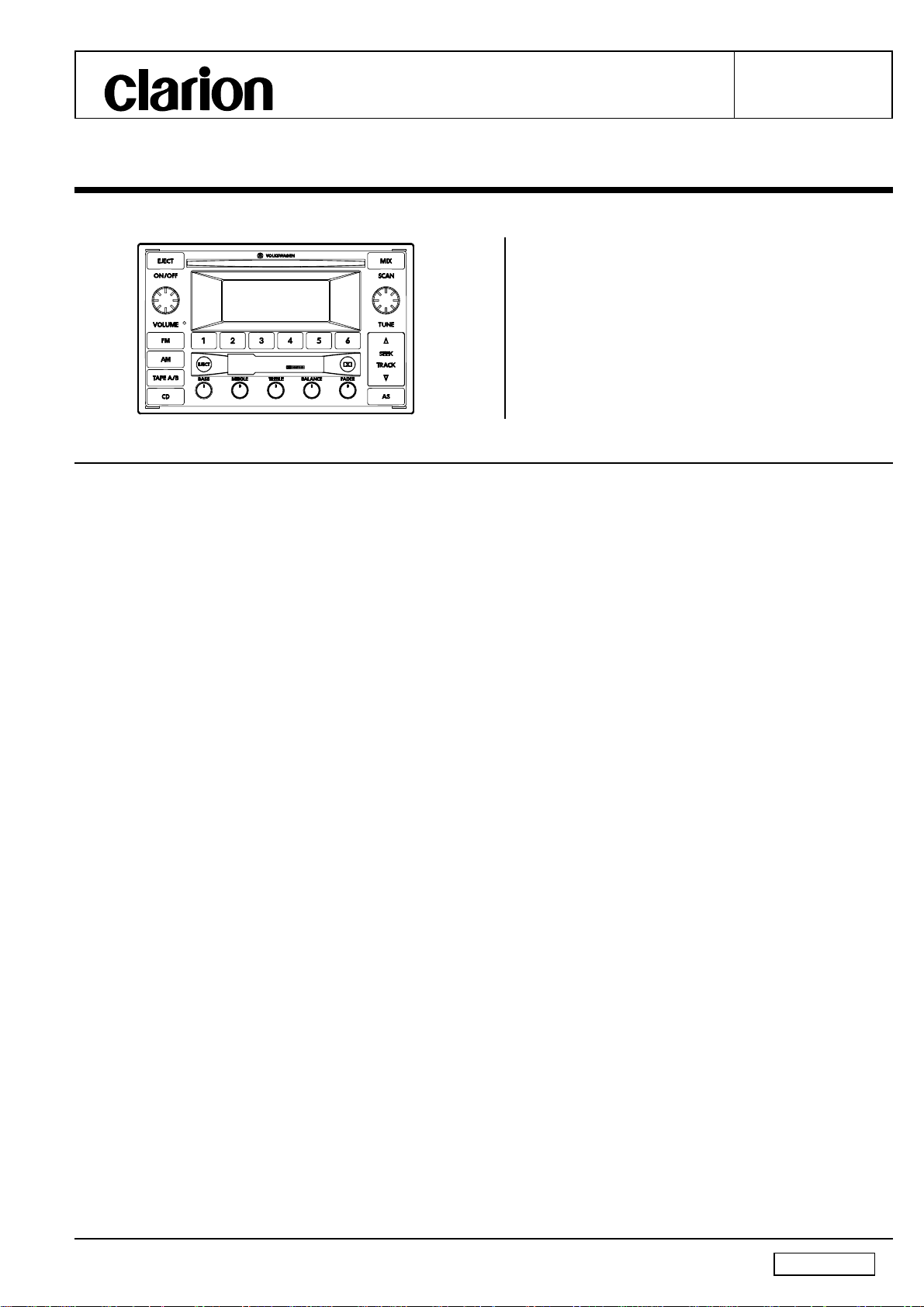
Genuine AM/FM Radio Cassette/
CD Stereo
Published by Service Dept.
298-5989-00
Printed in Japan
Jun.2002 P
■SPECIFICATIONS
Radio section
Tuning system: PLL frequency synthesizer system
Receive range: AM 530kHz to 1,710kHz
FM 87.9MHz to 107.9MHz
Intermediate frequency:
AM 450kHz
FM 10.7MHz
Quieting sensitivity: AM Less than 44dB
FM Less than 9dB
Separation: FM 25
Auto tuning stop sensitivity:
±5dB
AM 40dB
±3dBμ(DX)
FM 24
μ±3dBμ(DX)
Tape section
Reproducting system: 4 track,2 program
2 channel stereo system
Wow and flutter: Less than 0.3
Separation: More than 40dB
Cross talk: More than 40dB
S/N ratio: Normal tape(120
45dB/54dB(DOLBY B NR ON)
Metal tape(70
47dB/56dB(DOLBY B NR ON)
FF/REW time: Less than 120sec.(C-60)
μ(at 26dB S/N)
μ(at 30dB S/N)
%(W.R.M.S)
μs)
μs)
Model
PU-2354A
(Genuine No.3B7 035 180B)
General
Load impedance: 4Ω
Power output: More than 15W×4(at 5% dist.)
Power supply voltage: DC14.0V(10.8V to 15.6V)
Negative ground
Back-up consumption: Less than 2mA
Dimensions(mm): 179(W)
※ Dolby noise reduction manufactured under license from
Dolby Laboratories Licensing Corporation.
※ "DOLBY" and the double-D symbol are trademarks of
Dolby Laboratories Licensing Corporation.
※ Specifications and design are subject to change without
notice for further improvement.
×111.9(H)×174.5(D)
■COMPONENTS
PU-2354A-A
Main unit −−−−− 1
■NOTE
※ We cannot supply PWB with component parts in prin-
ciple. When a circuit on PWB has failure, please repair
it by component parts base. Parts which are not mentioned in service manual are not supplied.
※ This unit is used the special adjustment jig for measur-
ing.
CD section
Disc: 12cm,8cm Disc
Separation: More than 50dB
S/N ratio: More than 74dB
- 1 -
PU-2354A
■ To engineers in charge of repair or
inspection of our products.
Before repair or inspection, make sure to follow
the instructions so that customers and Engineers
in charge of repair or inspection can avoid suffering any risk or injury.
1. Use specified parts.
The system uses parts with special safety features against
fire and voltage. Use only parts with equivalent characteristics when replacing them.
The use of unspecified parts shall be regarded as remodeling for which we shall not be liable. The onus of
product liability (PL) shall not be our responsibility in cases
where an accident or failure is as a result of unspecified
parts being used.
2. Place the parts and wiring back in their original positions
after replacement or re-wiring.
For proper circuit construction, use of insulation tubes,
bonding, gaps to PWB, etc, is involved. The wiring connection and routing to the PWB are specially planned
using clamps to keep away from heated and high voltage
parts. Ensure that they are placed back in their original
positions after repair or inspection.
If extended damage is caused due to negligence during
repair, the legal responsibility shall be with the repairing
company.
3. Check for safety after repair.
Check that the screws, parts and wires are put back securely in their original position after repair. Ensure for
safety reasons there is no possibility of secondary
ploblems around the repaired spots.
If extended damage is caused due to negligence of repair, the legal responsibility shall be with the repairing
company.
4. Caution in removal and making wiring connection to the
parts for the automobile.
Disconnect the battery terminal after turning the ignition
key off. If wrong wiring connections are made with the
battery connected, a short circuit and/or fire may occur.
If extensive damage is caused due to negligence of repair, the legal responsibility shall be with the repairing
company.
5. Cautions regarding chips.
Do not reuse removed chips even when no abnormality
is observed in their appearance. Always replace them
with new ones. (The chip parts include resistors, capacitors, diodes, transistors, etc). The negative pole of tantalum capacitors is highly susceptible to heat, so use special care when replacing them and check the operation
afterwards.
6. Cautions in handling flexible PWB
Before working with a soldering iron, make sure that the
iron tip temperature is around 270
apply the iron tip repeatedly(more than three times)to the
same patterns. Also take care not to apply the tip with
force.
7. Turn the unit OFF during disassembly and parts replacement. Recheck all work before you apply power to the
unit.
8. Cautions in checking that the optical pickup lights up.
The laser is focused on the disc reflection surface through
℃. Take care not to
the lens of the optical pickup. When checking that the
laser optical diode lights up, keep your eyes more than
30cms away from the lens. Prolonged viewing of the laser within 30cms may damage your eyesight.
9. Cautions in handling the optical pickup
The laser diode of the optical pickup can be damaged by
electrostatic charge caused by your clothes and body.
Make sure to avoid electrostatic charges on your clothes
or body, or discharge static electricity before handling the
optical pickup.
9-1. Laser diode
The laser diode terminals are shorted for transportation in order to prevent electrostatic damage.
After replacement, open the shorted circuit. When
removing the pickup from the mechanism, short
the terminals by soldering them to prevent this
damage.
9-2. Actuator
The actuator has a powerful magnetic circuit. If a
magnetic material is put close to it. Its characteristics will change. Ensure that no foreign substances
enter through the ventilation slots in the cover.
9-3. Cleaning the lens
Dust on the optical lens affects performance. To
clean the lens, apply a small amount of isopropyl
alcohol to lens paper and wipe the lens gently.
■CAUTIONS
Use of controls,adjustment,or performance of procedures
other than those specified herein,may result in hazardous
radiation exposure.
The compact disc player should not be adjusted or repaired
by anyone except properly qualified service personnel.
■COMPUTER ANTI-THEFT SYSTEM
This unit has a built-in Computer Anti-theft System(CATS).
RELEASE the CATS
1. Turn power on.Then "SAFE" is indicated for 3
second.And then it change to indicate "1000".
2. Input code by M1 to M4 preset buttons.After selected
code,press SEEK up or SCAN button more than 2
second.Then beep sound is made.And then a unit work.
3. If wrong code is inputed 2 times,a unit will be lock by a
unit changes code input mode,it waits with power supply
for about 1 hour.
4. After lock 1 hour with power supply,it will be changed
code input mode.When wrong code is inputed twice, a
unit will be lock mode.
- 2 -PU-2354A
- 3 -
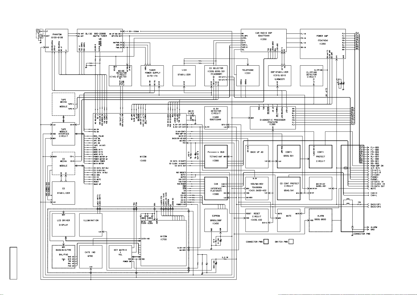
■BLOCK DIAGRAM
PU-2354A

■EXPLANATION OF IC
052-3156-90 MB90F594APF-G System Controller
1.Terminal Description
pin 1: POWER M- : O : Power motor control signal output.
pin 2: POWER M+ : O : Power motor control signal output.
pin 3: MECH POWER: O : Power ON signal output to the tape mech-
pin 4: MAIN MOTOR : O : "H"= Tape main motor ON.
pin 5: TAPE IN : - : Tape IN signal input.
pin 6: CLIP DET : IN : The clipping detection for the power am-
pin 7 : 6.5V DET : IN : 6.5V detection terminal.
pin 8 : 9.3V DET : IN : 9.3V detection terminal.
pin 9: MODE BIT 2 : IN : The mode bit input from the tape mecha-
pin 10: MODE BIT 1 :IN : The mode bit input from the tape mecha-
pin 11: VSS : - : Negative supply voltage.
pin 12: MODE BIT 3 :IN : The mode bit input from the tape mecha-
pin 13: VOL 1 : IN: Volume control pulse input from the rota-
pin 14: ES DATA Out : O : The serial data output to the display sec-
pin 15: ES CLOCK : O : The clock pulse output to the display sec-
pin 16: ES DATA IN :IN: The serial data input from the display sec-
pin 17: CD DI : IN : The serial data input from the CD mecha-
pin 18: CD CK Out : O : The clock pulse output to the CD mecha-
pin 19: CD DO : O : The serial data output to the CD mecha-
pin 20: EEP DO : O : The serial data output to EEP ROM.
pin 21: EEP CK : O : The clock pulse output to EEP-ROM.
pin 22: EEP DI : IN : The serial data input from EEP ROM.
pin 23: VCC : - : Positive supply voltage.
pin 24: CD/AC D I : IN : The serial data input from the CD auto
pin 25: CD/AC CK I :IN : The clock pulse input from the CD auto
pin 26: MUTE IN :IN : Mute command input.
pin 27: C CONNECT : - : The capacitor connection.
pin 28: ILL CNT 1 : O : Pulse output.
pin 29: ILL CNT 2 : O : Illumination ON signal of CAN BUS.
pin 30: DSP SDA :I/O: The serial data input/output for the digital
pin 31: NU : - : Not in use.
pin 32: DSP SCL : O : SCL output to the digital signal processor.
pin 33: DSP RESET : O : Reset signal output to the DSP IC.
pin 34: A VCC : - : Positive supply voltage for the internal
pin 35: A Vref+ : - : Reference voltage for the analog section.
pin 36: A Vref- : - : Reference voltage for the analog section.
pin 37: A VSS : - : Analog ground.
pin 38: FM MODULAT :IN : The input terminal of the internal ADC to
pin 39: FM NEIGHBOR: IN : The input terminal of the internal ADC to
pin 40: S METER :IN : The input terminal of internal A/D convert-
pin 41: MULTI PASS : IN : The input terminal of the internal ADC to
pin 42 : GND : - : Ground.
pin 43: LINE TEST : IN : The checking port.
pin 44: ROM Correct : IN: ROM correction port.
pin 45: BACKUP AD :IN : The input terminal of the internal ADC for
pin 46: CLIP AD I : IN : The input terminal of the internal ADC to
pin 47: DSP P ON MU: O : The power ON mute signal output to the
pin 48: CD/AC D O : O : The serial data output to the CD auto
pin 49: MODE 0 I :IN : Mode select input.
anism.
plifier.
nism.
nism.
nism.
ry encoder.
tion.
tion.
tion.
nism.
nism.
nism.
changer.
changer.
signal processor.
analog section.
detect FM modulation factor.
detect FM adjacent channel interference.
er to monitor the radio field strength.
detect the multi-pass.
the backup voltage detection.
detect the clipping of the speaker signal.
digital signal processor.
changer.
pin 50: MODE 1 I :IN : Mode select input.
pin 51: MODE 2 I :IN : Mode select input.
pin 52: HST IN : IN : The hardware standby.
pin 53 : GND : - : Ground.
pin 54: DIAG/TUN SD :I/O: Serial data communication line with the
pin 55: EEP CS P : O : The chip select signal output to EEP-ROM
pin 56: DIAG/TUN CK : O : Clock pulse output to the tuner pack.
pin 57: WARNING : IN : The warning signal input from the diagno-
pin 58: VCC : - : Positive supply voltage.
pin 59: STBY : O : The standby signal output.
pin 60: POWER LINE : O : 4 ohm speaker out = "H", Line out = "L".
pin 61: MAIN 14V : O : ON signal output to 14V power supply
pin 62: MAIN 5V : O : ON signal output to 5V power supply sec-
pin 63: D VSS : - : Digital ground.
pin 64: POWER ON : O : Power ON signal output.
pin 65: EEP CS : O : The chip select signal output to EEP-ROM.
pin 66: IF ON bk O : O : ON signal output to power supply section
pin 67: ES RESET : O : The reset pulse output to the display sec-
pin 68: D VCC : - : Positive supply voltage.
pin 69: CAN WAKE : O : The wake signal output to CAN IC.
pin 70: CAN ENABLE : O : The enable signal output to CAN IC.
pin 71: CAN STROBE : O : The strobe pulse output to CAN IC.
pin 72: CAN ERR I :IN: The error signal input from CAN IC.
pin 73: D VSS : - : Digital ground.
pin 74: CAN TX : O : CAN transmit.
pin 75: CAN RX : IN : CAN receve.
pin 76: CAN INH I : IN : The inhibit signal input from CAN IC.
pin 77: RST : IN : Reset signal input.
pin 78: ES SRQI :IN : SRQ input from the display section.
pin 79: POWER SW :IN : Power switch ON signal input.
pin 80: VOL 2 : IN: Volume control pulse input from the rota-
pin 81 : GND : - : Ground.
pin 82: X 0 : - : Crystal connection.
pin 83: X 1 : - : Crystal connection.
pin 84: VCC : - : Positive supply voltage.
pin 85: CD RESET : O : The reset pulse output to the CD IC.
pin 86: CD WAKE UP : O : The wake up signal output to the CD
pin 87: CD CS : O : The chip select signal output to the CD
pin 88: CD SRQ :IN: SRQ input from the CD mechanism.
pin 89: PHANTOM ON : O : ON signal output to power supply section
pin 90: DIAG CONT+ : IN : The diagnosis terminal.
pin 91: AM ON : O : AM ON signal output.
pin 92: FM ON : O : FM ON signal output.
pin 93: CD/AC SEL : O : CD/Auto-Changer select signal output.
pin 94: AMP MUTE : O : Muting signal output to the Audio Power
pin 95: AMP ON : O : Audio power amplifier ON signal output.
pin 96: FOW/REV : O : Forward/Reverse select output.
pin 97: METAL DET :IN: Metal tape detect signal input.
pin 98: APC DET I :IN: APC detected signal input.
pin 99: APC ON : O : APC ON signal output.
pin100: REEL PULSE : IN : Reel pulse input from the tape mechanism.
tuner pack.
for the patching.
sis IC.
section.
tion.
for fuba antenna.
tion.
ry encoder.
mechanism.
mechanism.
for phantom antenna.
Amplifier.
052-3157-90 MB90F583BPF-G Display Controller
1.Terminal Description
pin 1: KI 0 : IN : Key scan signal input.
pin 2: KI 1 : IN : Key scan signal input.
pin 3: KI 2 : IN : Key scan signal input.
pin 4: KI 3 : IN : Key scan signal input.
pin 5: KI 4 : IN : Key scan signal input.
pin 6: KI 5 : IN : Key scan signal input.
pin 7: KI 6 : IN : Key scan signal input.
pin 8: KI 7 : IN : Key scan signal input.
pin 9: LCD A0 : O : Data/Command distinction signal output to
- 4 -PU-2354A

LCD.
pin 10: LCD RD : O : Read command output to LCD.
pin 11: VSS : - : Negative supply voltage.
pin 12: LCD WR : O : Write command output to LCD.
pin 13: LCD CS : O : Chip select signal output to LCD.
pin 14: LCD RESET : O : Reset pulse output to LCD.
pin 15: NU : - : Not in use.
pin 16: NU : - : Not in use.
pin 17: MAIN REQ : O : REQ output to the main controller.
pin 18: MAIN DI : IN: The serial data input from the main con-
pin 19: NAIN DO : O : The serial data output to the main control-
pin 20: NU : - : Not in use.
pin 21: K O 0 : O : Key scan output terminal.
pin 22: K O 1 : O : Key scan output terminal.
pin 23: VCC : - : Positive supply voltage.
pin 24: K O 2 : O : Key scan output terminal.
pin 25: K O 3 : O : Key scan output terminal.
pin 26: NU : - : Not in use.
pin 27: C CONNECT : - : The capacitor connection.
pin 28: NU : - : Not in use.
pin 29: NU : - : Not in use.
pin 30: DAC REF : - : The reference voltage for the internal DAC.
pin 31: DAC VSS : - : The negative supply voltage for the inter-
pin 32: NU : - : Not in use.
pin 33: NU : - : Not in use.
pin 34: ADC VCC : - : The positive supply voltage for the inter-
pin 35: ADC Vref H : - : The higher reference voltage for the inter-
pin 36: ADC Vref L : - : The lower reference voltage for the inter-
pin 37: ADC VSS : - : The negative supply voltage for the inter-
pin 38: V LCD :IN : The input terminal of the internal ADC to
pin 39: FAD ADI : IN : The input terminal of the internal ADC to
pin 40: BAL ADI :IN: The input terminal of the internal ADC to
pin 41: NU : - : Not in use.
pin 42 : GND : - : Ground.
pin 43: NU : - : Not in use.
pin 44: TREB ADI : IN: The input terminal of the internal ADC to
pin 45: MID ADI : IN : The input terminal of the internal ADC to
pin 46: BASS ADI : IN : The input terminal of the internal ADC to
pin 47: TAPE EJECT : IN : Tape eject signal input.
pin 48: CD EJECT : IN: CD eject switch signal input.
pin 49: MODE 0 I :IN : Mode select input.
pin 50: MODE 1 I :IN : Mode select input.
pin 51: MODE 2 I :IN : Mode select input.
pin 52: HST IN : IN : The hardware standby.
pin 53: TUNE VOL 2 : IN: Tuning volume switch pulse input.
pin 54: TUNE VOL 1 : IN: Tuning volume switch pulse input.
pin 55: NU : - : Not in use.
pin 56: NU : - : Not in use.
pin 57: WAKE UP : IN : Wake up signal input.
pin 58: 6.5V DET : IN : 6.5V detection terminal.
pin 59: EEP DI : IN : The serial data input from EEP-ROM.
pin 60: EEP DO : O : The serial data output to EEP-ROM.
pin 61: EEP CK : O : The clock pulse output to EEP-ROM.
pin 62: EEP CEO : O : The chip enable signal output to EEP-
pin 63: NU : - : Not in use.
pin 64: NU : - : Not in use.
pin 65: NU : - : Not in use.
pin 66: NU : - : Not in use.
pin 67: NU : - : Not in use.
pin 68: NU : - : Not in use.
pin 69: NU : - : Not in use.
troller.
ler.
nal DAC.
nal ADC.
nal ADC.
nal ADC.
nal ADC.
sense the temperature signal voltage of
LCD.
sense the fader control voltage.
sense the balance control voltage.
sense the treble control voltage.
sense the middle control voltage.
sense the bass control voltage.
ROM.
pin 70: NU : - : Not in use.
pin 71: NU : - : Not in use.
pin 72: NU : - : Not in use.
pin 73: NU : - : Not in use.
pin 74: NU : - : Not in use.
pin 75: NU : - : Not in use.
pin 76: NU : - : Not in use.
pin 77: RESET : IN : Reset signal input.
pin 78: CATS IND : O : CATS indicator control signal output.
pin 79: X OUT : O : Crystal connection.
pin 80: X IN : IN : Crystal connection.
pin 81: VSS : - : Negative supply voltage.
pin 82: X IN : IN : Crystal connection.
pin 83: X OUT : O : Crystal connection.
pin 84: VCC : - : Positive supply voltage.
pin 85: No Exp : - : No explanation.
pin 86: No Exp : - : No explanation.
pin 87: NU : - : Not in use.
pin 88: NU : - : Not in use.
pin 89: NU : - : Not in use.
pin 90: NU : - : Not in use.
pin 91: NU : - : Not in use.
pin 92: NU : - : Not in use.
pin 93: D 0 :I/O: Data input/output.
pin 94: D 1 :I/O: Data input/output.
pin 95: D 2 :I/O: Data input/output.
pin 96: D 3 :I/O: Data input/output.
pin 97: D 4 :I/O: Data input/output.
pin 98: D 5 :I/O: Data input/output.
pin 99: D 6 :I/O: Data input/output.
pin100: D 7 :I/O: Data input/output.
052-5043-01 MN101C309CA CD Mechanism Controller
1.Terminal Description
pin 1 : KEY3bk : IN : For the test.
pin 2 : KEY4bk : IN : For the test.
pin 3: NU : - : Not in use.
pin 4: NU : - : Not in use.
pin 5: NU : - : Not in use.
pin 6: Vref : - : Reference voltage.
pin 7: VDD : - : Positive supply voltage.
pin 8 : OSC2bk : - : OSC
pin 9 : OSC1bk : - : OSC
pin 10: VSS : - : Negative supply voltage.
pin 11: NU : - : Not in use.
pin 12: NU : - : Not in use.
pin 13: NU : - : Not in use.
pin 14: SDObk : O : Communication line with the main section.
pin 15: SDIbk : IN : Communication line with the main section.
pin 16: SCKbk :IN : Communication line with the main section.
pin 17: NU : - : Not in use.
pin 18: SUBQbk : IN : Communication line with CD IC.
pin 19: SQCKbk : O : Communication line with CD IC.
pin 20: NU : - : Not in use.
pin 21: RESETbk : IN : Communication line with the main section.
pin 22: MUTEbk : O : Communication line with the main section.
pin 23: CSbk : IN : Communication line with the main section.
pin 24: SRQbk : O : Communication line with the main section.
pin 25: SYSP1bk : IN : Communication line with the main section.
pin 26: SYSP2bk : O : Communication line with the main section.
pin 27: WPbk : IN : Communication line with the main section.
pin 28: Blkck/Dqsy bk :IN : Communication line with CD IC.
pin 29: NU : - : Not in use.
pin 30: NU : - : Not in use.
pin 31: NU : - : Not in use.
pin 32: NU : - : Not in use.
pin 33: NU : - : Not in use.
pin 34: NU : - : Not in use.
pin 35: SensorCbk :IN : Mechanism control.
pin 36: SensorBbk : IN : Mechanism control.
pin 37: SensorAbk : IN : Mechanism control.
pin 38: CHUSWbk : IN : Mechanism control.
- 5 -
PU-2354A

pin 39: MCCWbk : O : Mechanism control.
pin 40: MCWbk : O : Mechanism control.
pin 41: LIMITbk : IN : Mechanism control.
pin 42: NFLOCKbk : O : Monitor terminal.
pin 43: NTLOCKbk : O : Monitor terminal.
pin 44: RESYbk : O : Monitor terminal.
pin 45: NU : - : Not in use.
pin 46: NU : - : Not in use.
pin 47: NU : - : Not in use.
pin 48: NU : - : Not in use.
pin 49: NU : - : Not in use.
pin 50: NU : - : Not in use.
pin 51: NU : - : Not in use.
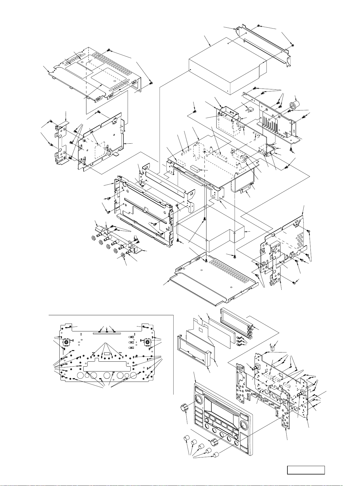
■EXPLODED VIEW・PARTS LIST
Main section
1 940-7921-01 ESCUTCHEON ASSY 1
2 380-5513-00 KNOB 2
3 380-5495-00 KNOB 5
4 345-8518-00 RUBBER SWITCH 1
5 039-1801-00 SWITCH PWB 1
6 331-2998-00 LCD COVER 1
7 379-0459-00 INDICATOR 1
8 335-6746-00 DIFFUSER 1
9 335-6383-00 ILLUMI-PLATE 1
10 001-7035-02 LED 3
11 335-6381-00 LCD-HOLDER 1
12 016-0022-00 ROTARY ENCODER 1
13 016-0021-00 ROTARY ENCODER 1
14 074-1059-76 OUTLET SOCKET(26P) 2
15 076-0567-03 PLUG(3P) 1
16 074-1151-20 OUTLET SOCKET(20P) 1
17 013-7104-00 SWITCH 1
18 076-0567-07 PLUG(7P) 1
19 716-0778-00 WAVE SCREW 12
20 722-0603-00 NUT 5
21 016-4155-00 VARIABLE RESISTOR 5
22 076-0540-08 PLUG(8P) 1
23 331-2997-00 VR-HOLDER 1
24 076-0570-07 PLUG(7P) 1
25 309-0761-01 FRONT PLATE 1
26 305-0299-00 SIDE PLATE 1
27 305-0300-02 SIDE PLATE(R) 1
28 750-3414-01 SIDE SPRING 2
29 304-0469-00 LOWER COVER 1
30 303-0476-00 UPPER COVER 1
31 930-0800-50 TAPE MECHANISM 1
32 929-0095-50 CD MECHANISM 1
33 331-2993-00 MECH-BRKT 1
34 331-2994-00 MECH-BRKT 1
35 076-0570-03 PLUG(3P) 1
(WITHOUT COMPONENT)
pin 52: NU : - : Not in use.
pin 53: NU : - : Not in use.
pin 54: NU : - : Not in use.
pin 55: NRSTbk : O : Communication line with CD IC.
pin 56: DMUTEbk : O : Communication line with CD IC.
pin 57: MLDbk : O : Communication line with CD IC.
pin 58: MDATAbk : O : Communication line with CD IC.
pin 59: MCLKbk : O : Communication line with CD IC.
pin 60: STATbk : IN: Communication line with CD IC.
pin 61 : GND : - : Ground.
pin 62: KEY0bk : IN : For the test.
pin 63: KEY1bk : IN : For the test.
pin 64: KEY2bk : IN : For the test.
NO. PART NO. DESCRIPTION Q'TYNO. PART NO. DESCRIPTION Q'TY
36 039-1799-01 MAIN PWB 1
(WITHOUT COMPONENT)
37 331-2991-00 MECH-BRKT 1
38 331-2992-00 MECH-BRKT 1
39 331-2990-00 IC-HOLDER 1
40 051-2036-00 IC(TDA7454) 1
41 076-0641-10 PLUG(10P) 1
42 039-1800-00 CONNECTOR PWB 1
(WITHOUT COMPONENT)
43 331-2995-00 OUTLET HOLDER 1
44 074-1262-00 OUTLET SOCKET 1
45 331-3220-00 ANT-HOLDER 1
46 076-0641-16 PLUG(16P) 1
47 060-8021-06 AUTO FUSE(10A) 1
48 313-1797-02 HEAT SINK 1
49 290-7914-00 LABEL 1
50 290-7913-00 LABEL 1
51 286-9433-00 SETPLATE 1
52 290-7885-00 BAR CODE LABEL 1
53 714-2606-81 MACHINE SCREW(M2.6×6) 28
54 714-3006-40 MACHINE SCREW(M3×6) 4
55 714-2303-81 MACHINE SCREW(M2.3×3) 4
56 716-1573-00 SCREW 4
57 290-8022-00 GUIDE LABEL 1
58 076-0640-18 PLUG(18P) 1
59 074-1151-08 OUTLET SOCKET(8P) 1
60 001-7048-91 LED 20
61 092-4300-10 ANT-RECEPTACLE 1
62 092-4301-10 ANT-RECEPTACLE 1
63 076-0433-20 PLUG(20P) 1
64 076-0540-20 PLUG(20P) 1
65 076-0641-24 PLUG(24P) 1
66 076-0324-05 PLUG(5P) 1
67 345-7496-00 REAR HOLDER 1
68 001-7031-81 LED 15
69 880-2088B FM/AM TUNER 1
- 6 -PU-2354A
54
30
50
28
49
52
53
57
22
25
53
23
55
53
33
26
53
64
24
35
55
36
53
32
42
41
63
58
43
34
37
47
65
44
38
46
69
39
40
66
42
55
62
53
61
45
67
53
48
53
27
68
60
60
68
60
68
20
60
56
21
31
53
5
53
51
53
54
29
9
8
53
28
11
68
17
10
60
12
1
7
16
6
19
14
19
18
- 7 -
19
59
15
13
2
5
4
3
PU-2354A
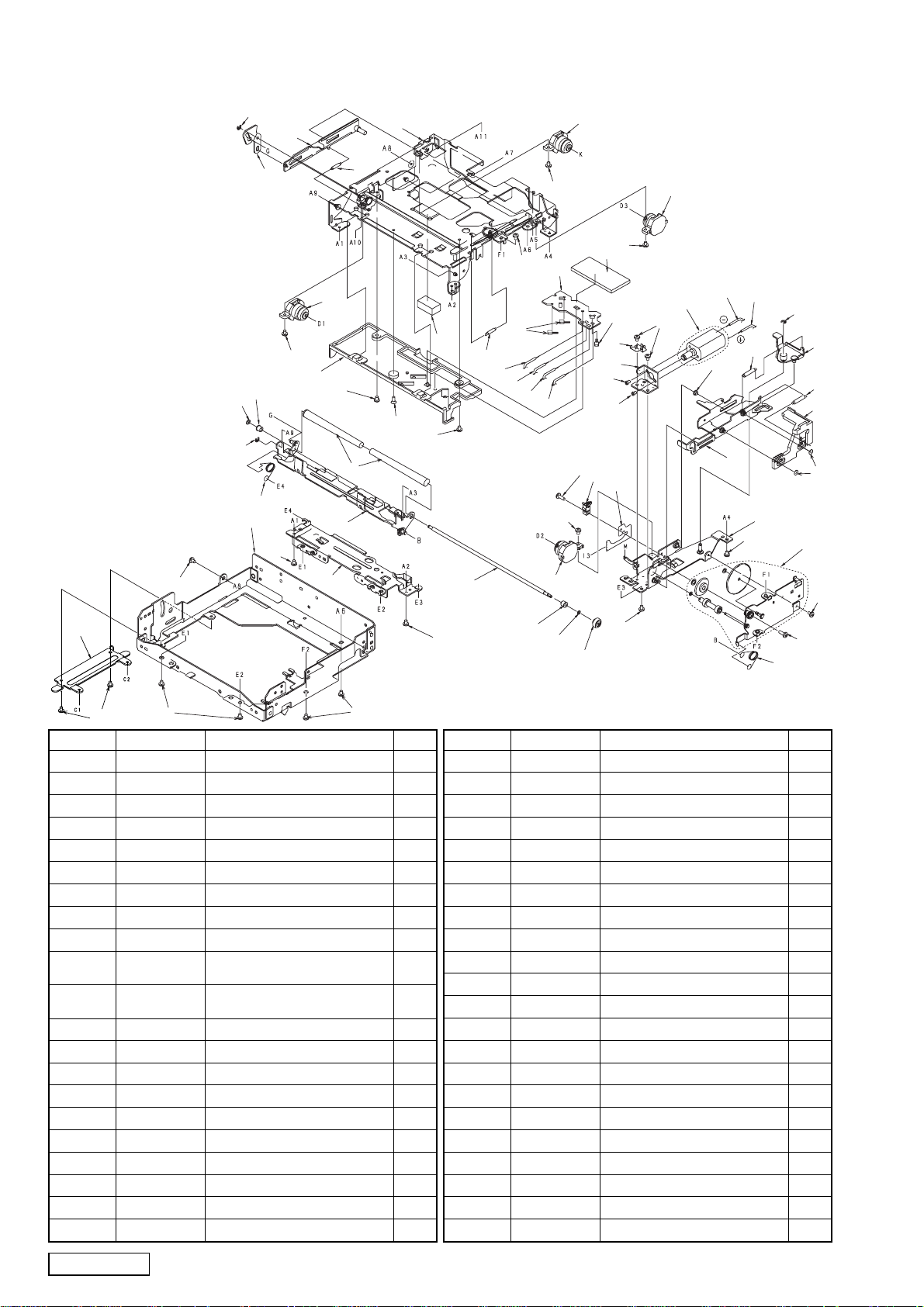
CD mechanism:Mechanism chassis section
929-0095-50
39
6
49
32
48
39
37
22
25
35
17
50
51
24
16
32
44
27
51
51
50
29
12
9
21
15
23
32
13
43
44
40
1
45
14
11
12
18
20
46
46
41
8
10
51
50
32
26
47
19
33
4
50
39
5
28
30
36
2
3
50
7
52
50
1 966-0309-23 L-DISC-G-ASSY 1
2 966-0310-41 SHIFT-P-CH-ASSY 1
3 HBS-430-100 GEAR PALTE ASSY 1
4 966-0312-41 SHIFT PLATE ASSY 1
5 966-0358-41 DRIVE-L ASSY 1
6 966-0359-41 SIDE-L PLATE ASSY 1
7 SMA-147-100 MOTOR ASSY(LOADING) 1
8 013-3879-01 CHUCKING SWITCH 1
9 804-4910-60 LEAD WIRE(YEL) 1
10 039-0586-50 CHUCKING SWITCH PWB 1
11 039-0588-01 SENSOR PWB 1
12 060-0252-01 PHOTO TR 3
13 345-7513-01 CLAMPER SHEET 1
14 345-7514-00 SENSOR PWB SHEET 1
15 802-4910-60 LEAD WIRE(RED) 1
16 620-0485-20 FRONT PLATE 1
17 620-0488-40 S-L LINK PLATE 1
18 620-0489-40 MOTOR PLATE 1
19 802-4904-60 LEAD WIRE(RED) 1
20 620-0492-20 MOTOR BRACKET 1
21 801-4910-60 LEAD WIRE(BRN) 1
48
(WITHOUT COMPONENT)
(WITHOUT COMPONENT)
48
50
NO. PART NO. DESCRIPTION Q'TYNO. PART NO. DESCRIPTION Q'TY
22 620-0773-40 CD MECHA. BRKT 1
23 800-4910-60 LEAD WIRE(BLK) 1
24 621-0402-50 U-DISC GUIDE-F 1
25 621-0243-50 ROLLER SLEEVE 2
26 800-4904-60 LEAD WIRE(BLK) 1
27 750-3189-00 SIDE-L SPRING 1
28 750-3098-00 L-LINK SPRING 1
29 750-3094-00 S ARM SPRING 1
30 621-0248-51 RACK GEAR 1
31 621-0249-50 ROLLER GEAR 1
32 629-0079-00 DAMPER 4
33 750-3092-03 SHIFT SPRING 1
34 750-3091-03 LOADING SPRING-R 1
35 750-3090-02 LOADING SPRING-L 1
36 746-0877-02 WASHER 2
37 746-0762-00 WASHER 1
38 746-0712-03 WASHER 1
39 743-1500-10 E-RING 3
40 621-0258-97 LOADING ROLLER 2
41 716-1742-00 SCREW(M2×5) 1
42 716-1704-00 SCREW(M2×7) 1
43 716-1677-00 SCREW(M2×5) 1
25
38
50
31
42
34
- 8 -PU-2354A
 Loading...