


Clarion |
( Malaysia) Sdn. Bhd. |
|
Published by Clarion (Malaysia) |
|
Phase 3, Free Trade Zone One, 11900 Bayan Lepas, Penang, Malaysia |
|
|||
|
298-6124-00 FEB. 2004P |
|||
Tel: (60) 4-6148-400, Fax: (60) 4-6439-108 |
|
|||
Clarion |
Co. |
Ltd. |
|
Printed In Malaysia |
Export Division : |
50 Kamitoda, Toda-shi, Saitama 335-8511 Japan |
|
|
|
|
|
|
|
|
|
|
Service |
Manual |
|
|
|
|
|
|
AM/FM CD/MP3 Player
Model
(PE-2640B-A: For U.S.A.)
Model
(PE-2640K-A: For other countries)
SPECIFICATIONS
Radio section Model: PE-2640B-A
Tuning system: PLL synthesizer tuner
Receiving frequencies: FM 87.9 to 107.9MHz (0.20 MHz steps) AM 530 to 1,710kHz (10 kHz steps)
Model: PE-2640K-A
Tuning system: |
PLL synthesizer tuner |
|
Receiving frequencies: |
FM 87.0 to 108MHz (0.05 MHz steps) |
|
|
AM 531 to 1,629kHz (9 kHz steps) |
|
CD/MP3 player section |
|
|
System: |
Compact disc digital audio system |
|
Frequency response: |
10Hz to 20kHz (+1dB/-1dB) |
|
Signal to Noise ratio: |
100dB (1kHz) IHF-A |
|
Dynamic range: |
95dB (1kHz) |
|
Distortion: |
0.01% |
|
MP3 |
|
|
Decode Format: |
MPEG 1, 2 and 2.5-Layer 3 |
|
Sampling rate (kHz): |
MPEG-1: |
32, 44.1, 48 |
|
MPEG-2: |
16, 22.05, 24 |
|
MPEG-2.5: |
8, 11.025, 24 |
Bit-rate (kbps): |
8, 16, 24, 32, 40, 48, 56, 64, 80, 96, 112, |
|
|
128, 144, 160, 192, 224, 256, 320, VBR |
|
CD-ROM Format: |
ISO9660 Level 1, 2, Romeo and Joliet |
|
Folder Level Limit: |
No limitation |
|
Folder Support: |
128 |
|
File Support: |
254 |
|
Folder Name: |
Maximum 16 characters |
|
File Name: |
Maximum 28 characters |
|
General |
|
|
Max. Power Output: |
50W x 4 |
|
Line Output: |
1.7V (with CD 1kHz, 10k ohm) |
|
Bass Control Action: |
+14dB/-14dB (30Hz) |
|
Treble Control Action: |
+14dB/-14dB (10 kHz) |
|
Power supply voltage: |
DC 14.4V (10.8 to 15.6V allowable) |
|
|
negative ground |
|
Current consumption: |
Less than 15A |
|
Speaker impedance: |
4 ohm (4 ohm to 8 ohm allowable) |
|
Dimensions (mm): |
178 (W) x 50 (H) x 152 (D)mm |
|
Weight: |
1.1kg |
|

 Specification and design are subject to change without notice for further improvement.
NOTE
1.We cannot supply PWB with component parts in principle. When a circuit on PWB has failure, please repair it by component parts base. Parts which are not mentioned in service manual are not supplied.
FEATURES
1.Visible Blue Negative LCD and White Illuminated Buttons
2.Aluminium Detachable Faceplate
3.Rotary Volume for Easy Operation
4.Z-Enhancer with 3 Mode Sound Selector
5.MAGNA BASS EX for Dynamic Bass Tuning
6. FM Reception System
7.Seek/Manual Up/Down Tuning
8.8-Times Oversampling Digital Filter and Dual 1-Bit D/A Converters
9.Preset Station Scan (PS), Automatic Store (AS)
10.4-Channel RCA Line Level Output
11.AM 1 band, FM 3 bands each 6 channels total 24 channels, Preset Memory Function
12.Repeat/Random Play/Intro Music Scan
13.200W (50 W x 4) Maximum Power Output
14.IR Remote Control Included
15.MP3NAVI for Quick Music Folder and Track Search
16 MP3 File Playable with ID3-TAG Display
COMPONENTS
PE-2640B-A / PE-2640K-A
Source unit |
|
|
1 |
|
|
|
|||
Battery (SUM-3) |
|
|
|
|
(PE-2640B only) |
|
|
2 |
|
|
|
|||
Remote Controller |
|
|
|
|
(PE-2640B only) |
RCB-164-201 |
1 |
||
DCP Case |
335-5734-05 |
1 |
||
Mounting bracket |
300-7742-20 |
1 |
||
Escutcheon (Outer-Es) |
|
|
|
|
(PE-2640B) |
370-6100-00 |
1 |
||
(PE-2640K) |
370-6096-00 |
1 |
||
Extension Lead |
854-6391-60 |
1 |
||
Part’s bag |
|
|
|
1 |
|
|
|
||
Removal key |
331-2497-20 |
2 |
||
Stopper (PE-2640B only) |
335-4899-20 |
1 |
||
- 1 - |
DB345MP/DB346MP |

To engineers in charge of repair or inspection of our products.
Before repair or inspection, make sure to follow the instructions so that customers and Engineers in charge of repair or inspection can avoid suffering any risk or injury.
1.Use specified parts.
The system uses parts with special safety features against fire and voltage. Use only parts with equivalent characteristics when replacing them.
The use of unspecified parts shall be regarded as remodeling for which we shall not be liable.The onus of product liability (PL) shall not be our responsibility in cases where an accident or failure is as a result of unspecified parts being used.
2.Place the parts and wiring back in their original positions after replacement or re-wiring.
For proper circuit construction, use of insulation tubes, bonding, gaps to PWB, etc., is involved. The wiring con-
nection and routing to the PWB are specially planned using clamps to keep away from heated and high voltage parts. Ensure that they are placed back in their original positions after repair or inspection.
If extended damage is caused due to negligence during repair, the legal responsibility shall be with the repairing company.
3. Check for safety after repair.
Check that the screws, parts and wires are put back securely in their original position after repair. Ensure for safety reasons there is no possibility of secondary problems around the repaired spots.
If extended damage is caused due to negligence of repair, the legal responsibility shall be with the repairing company.
4.Caution in removal and making wiring connection to the parts for the automobile.
Disconnect the battery terminal after turning the ignition key off. If wrong wiring connections are made with the battery connected, a short circuit and/or fire may occur. If extensive damage is caused due to negligence of repair, the legal responsibility shall be with the repairing company.
5.Cautions regarding chips.
Do not reuse removed chips even when no abnormality is observed in their appearance. Always replace them with new ones. (The chip parts include resistors, capacitors, diodes, transistors, etc.). The negative pole of tantalum capacitors is highly susceptible to heat, so use special care when replacing them and check the operation afterwards.
6.Cautions in handling flexible PWB.
Before working with a soldering iron, make sure that the iron tip temperature is around 270°C. Take care not to apply the iron tip repeatedly (more than three times) to the same patterns. Also take care not to apply the tip with force.
7.Turn the unit OFF during disassembly and parts replacement. Recheck all work before you apply power to the unit.
8.Cautions in checking that the optical pickup lights up. The laser is focused on the disc reflection surface through the lens of the optical pickup. When checking that the laser optical diode lights up, keep your eyes more than 30cm away from the lens. Prolonged viewing of the laser within 30cm may damage your eyesight.
9.Cautions in handling the optical pickup
The laser diode of the optical pickup can be damaged by electrostatic charge caused by your clothes and body. Make sure to avoid electrostatic charges on your clothes or body, or discharge static electricity before handling the optical pickup.
9-1.Laser diode
The laser diode terminals are shorted for transportation in order to prevent electrostatic damage. After replacement, open the shorted circuit. When removing the pickup from the mechanism, short the terminals by soldering them to prevent this damage.
9-2.Actuator
The actuator has a powerful magnetic circuit. If a magnetic material is put close to it. Its characteristics will change. Ensure that no foreign substances enter through the ventilation slots in the cover.
9-3.Cleaning the lens
Dust on the optical lens affects performance. To clean the lens, apply a small amount of isopropyl alcohol to lens paper and wipe the lens gently.
CAUTIONS
Use of controls, adjustments, or performance of procedures other those specified herein, may result in hazardous radiation exposure.
The compact disc player should not be adjustment or repaired by anyone except properly qualified service personnel.
Bottom View of
Main Unit
DB345MP/DB346MP |
- 2 - |
TROUBLESHOOTING
Problem |
|
Cause |
Measure |
||
Power does not turn on. |
Fuse is |
blown. |
Replace with a fuse of the same amperage. |
||
(No sound is |
produced). |
|
|
|
|
Incorrect |
wiring |
Read the attached “Installation/Wire connection |
|||
|
|
||||
|
|
|
|
Guide” once again and wire properly. |
|
|
|
|
|
||
Compact disc |
cannot be |
Another compact disc is already |
Eject the compact disc before loading the new |
||
loaded. |
|
loaded. |
|
one. |
|
|
|
|
|
|
|
|
|
Compact |
disc is dirty. |
Clean the compact disc with a soft cloth. |
|
Sound skips or is noisy. |
|
|
|||
Compact disc is heavily scratched |
Replace with a compact disc with no scratches. |
||||
|
|
or warped. |
|
||
|
|
|
|||
Sound is bad directly after |
Water droplets may form on the |
Let dry for about 1 hour with the power on. |
|||
power is turned on. |
internal lens when the car is |
|
|||
|
|
parked in a humid place. |
|
||
|
|
|
|||
Nothing happens when buttons |
Microprocessor has |
Turn off the power, then press the [RELEASE] |
|||
are pressed. |
|
malfunctioned due to noise, etc. |
button and remove the DCP. |
||
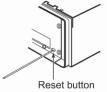
Display is not |
accurate. |
|
|
Press the reset button for about 2 seconds with a |
|
|
|
|
|
thin rod. |
|
|
|
|
|
||
|
|
DCP or main unit connectors are |
Wipe the dirt off with a soft cloth moistened with |
||
|
|
dirty. |
|
cleaning alcohol. |
|
|
|
|
|
|
|
ERROR DISPLAYS
To protect the system, this unit has been equipped with self diagnostic functions. If a fault arises, a warning is issued by various error displays. Follow the corrective measures and remove the fault.
Error Display |
Corrective Measure |
|
|
|
|
ER2 |
This error display indicates that a fault has arised in the mechanism of the |
|
source unit (for example, the disc cannot be ejected). |
||
!Check the source unit |
||
|
||
|
|
|
ER3 |
This error display indicates that the pickup focus is off because of a scratched |
|
disc or some other factor during source unit play. |
||
|
!Check the compact unit |
|
|
|
|
ER6 |
This indicates that the CD’s TOC (table of contents) cannot be read, because |
|
the selected disc is upside-down. |
||
|
|
- 3 - |
DB345MP/DB346MP |

BLOCK DIAGRAM
MAIN UNIT SECTION
CD MECHANISM SECTION 929-0290-80
DB345MP/DB346MP |
- 4 - |

EXPLANATION OF IC
uPD784215AYGC-129-8EU |
052-3933-00 |
|
|
|||||||||
Master Micro |
computer |
|
|
|
|
|
|
|
||||
|
|
|
|
|
|
|
|
|
|
|
|
|
Outward |
Form |
|
|
|
|
|
|
|
|
|
||
100 pins, |
plastic |
QFP |
|
|
|
|
|
|
|
|
||
Terminal |
Description |
|
|
|
|
|
|
|
|
|||
|
|
|
|
|
|
|
|
|||||
Pin No |
|
PIN NAME |
I/O |
DESCRIPTION |
|
|
|
|||||
|
|
|
|
|
|
|
||||||
1 |
|
VOL_CLK |
O |
E-VOL |
Control Clock output |
|||||||
|
|
|
|
|
|
|||||||
2 |
|
VOL_DATA |
O |
E-VOL Control Data output |
||||||||
|
|
|
|
|
|
|||||||
3 |
|
REM_DET |
I |
While protecting circuit motion, it |
||||||||
|
|
|
|
|
|
is at |
‘HI’ |
|
|
|
|
|
|
|
|
|
|
|
|||||||
4 |
|
OFFSET DET |
I |
While Power Amp IC is abnormal, |
||||||||
|
|
|
|
|
|
it is at |
‘LOW’ |
|
|
|
||
|
|
|
|
|
|
|
|
|
|
|
||
5 |
|
PHONE_INT |
I |
NC |
|
|
|
|
|
|
||
|
|
|
|
|
|
|
|
|
|
|
|
|
6 |
|
NC |
|
|
- |
NC |
|
|
|
|
|
|
|
|
|
|
|
|
|||||||
7 |
|
MP3 REQ |
I |
REQ input from MP3 decoder |
||||||||
|
|
|
|
|
|
|
|
|
|
|
|
|
8 |
|
NC |
|
|
- |
NC |
|
|
|
|
|
|
|
|
|
|
|
|
|
|
|||||
9 |
|
VDD |
|
|
- |
Power supply terminal 5V |
||||||
|
|
|
|
|
|
|
|
|
|
|||
10 |
|
X_OUT |
|
- |
Crystal |
12MHz |
(Main |
system |
||||
|
|
|
|
|
|
clock) |
|
|
|
|
|
|
|
|
|
|
|
|
|
|
|
|
|||
11 |
|
X_IN |
|
- |
Crystal |
12MHz |
(Main |
system |
||||
|
|
|
|
|
|
clock) |
|
|
|
|
|
|
|
|
|
|
|
|
|
|
|
|
|
|
|
12 |
|
VSS |
|
|
- |
GND |
|
|
|
|
|
|
|
|
|
|
|
|
|
|
|
|
|
||
13 |
|
XT_OUT |
- |
NC |
|
|
|
|
|
|
||
|
|
|
|
|
|
|
|
|
|
|
|
|
14 |
|
XT_IN |
|
- |
GND |
|
|
|
|
|
|
|
|
|
|
|
|
|
|
||||||
15 |
|
RESET |
|
- |
Reset port (When system is |
|||||||
|
|
|
|
|
|
reset, it is at ‘LOW’) |
|
|
||||
|
|
|
|
|
|
|
|
|
|
|
|
|
16 |
|
NC |
|
|
- |
NC |
|
|
|
|
|
|
|
|
|
|
|
|
|
|
|||||
17 |
|
B/U |
DET |
I |
B/U detecting terminal |
|
|
|||||
|
|
|
|
|
|
|
||||||
18 |
|
ACC |
DET |
I |
ACC detecting terminal |
|||||||
|
|
|
|
|
|
|||||||
19 |
|
REMOCON |
I |
IR Sensor signal input for Remote |
||||||||
|
|
|
|
|
|
Control |
|
|
|
|
|
|
|
|
|
|
|
|
|||||||
20 |
|
KEY_INT |
I |
When this terminal turns low, key |
||||||||
|
|
|
|
|
|
A/D terminal detects the key |
||||||
|
|
|
|
|
|
pushed (FNC, EJECT & DCP |
||||||
|
|
|
|
|
|
keys) |
|
|
|
|
|
|
|
|
|
|
|
|
|
||||||
21 |
|
SBSY |
|
I |
GS1-MC CD Sub-code block |
|||||||
|
|
|
|
|
|
sync |
detection input |
|
|
|||
|
|
|
|
|
|
|
||||||
22 |
|
TBASE |
|
I |
PLL Time Base signal input (8Hz) |
|||||||
|
|
|
|
|
|
|
||||||
23 |
|
AVDD |
|
- |
Analog Power supply 5V |
|||||||
|
|
|
|
|
|
|||||||
24 |
|
AVREF0 |
- |
ADC Reference Voltage Input |
||||||||
|
|
|
|
|
|
|||||||
25 |
|
KEY A/D |
I |
FNC/EJECT/DCP detection |
||||||||
|
|
|
|
|
|
terminal |
for |
A/D |
converter |
|||
|
|
|
|
|
|
|
|
|
||||
26 |
|
TEST |
|
I |
TEST keys |
detection |
terminal |
|||||
|
|
|
|
|
|
(For |
Test Mode |
purpose) |
||||
|
|
|
|
|
|
|
|
|
|
|
|
|
27 |
|
NC |
|
|
- |
NC |
|
|
|
|
|
|
|
|
|
|
|
|
|
|
|
|
|
|
|
28 |
|
NC |
|
|
- |
NC |
|
|
|
|
|
|
|
|
|
|
|
|
|
|
|
|
|
|
|
29 |
|
NC |
|
|
- |
NC |
|
|
|
|
|
|
|
|
|
|
|
|
|
|
|
|
|
|
|
30 |
|
NC |
|
|
- |
NC |
|
|
|
|
|
|
|
|
|
|
|
|
|
|
|
|
|
|
|
31 |
|
NC |
|
|
- |
NC |
|
|
|
|
|
|
|
|
|
|
|
|
|
|
|
|
|
|
|
32 |
|
NC |
|
|
- |
NC |
|
|
|
|
|
|
|
|
|
|
|
|
|
|
|
||||
33 |
|
AVSS |
|
- |
Analog GND |
|
|
|
||||
|
|
|
|
|
|
|
|
|
|
|
|
|
Pin No |
PIN NAME |
I/O |
DESCRIPTION |
|
||||
|
|
|
|
|
|
|
|
|
34 |
NC |
- |
NC |
|
|
|
|
|
|
|
|
|
|
|
|
|
|
35 |
NC |
- |
NC |
|
|
|
|
|
|
|
|
|
|||||
36 |
AVREF1 |
- |
DAC Reference Voltage Input |
|||||
37 |
NC |
- |
NC |
|
|
|
|
|
|
|
|
|
|
|
|
|
|
38 |
NC |
- |
NC |
|
|
|
|
|
|
|
|
|
|
|
|
|
|
39 |
NC |
- |
NC |
|
|
|
|
|
|
|
|
|
|
|
|
|
|
40 |
NC |
- |
NC |
|
|
|
|
|
|
|
|
|
|
|
|
|
|
41 |
NC |
- |
NC |
|
|
|
|
|
42 |
NC |
- |
NC |
|
|
|
|
|
|
|
|
|
|
|
|
|
|
43 |
NC |
- |
NC |
|
|
|
|
|
|
|
|
|
|
|
|
|
|
44 |
NC |
- |
NC |
|
|
|
|
|
|
|
|
|
|||||
45 |
MP3 SDA |
I/O |
MP3 Data Communication Port |
|||||
|
|
|
(I2C |
bus) |
|
|
|
|
|
|
|
|
|
|
|
|
|
46 |
NC |
- |
NC |
|
|
|
|
|
|
|
|
|
|||||
47 |
MP3 SCL |
O |
MP3 Clock Output (I2C bus) |
|||||
|
|
|
|
|||||
48 |
MP3 RESET |
O |
When MP3 decoder is reset, it is |
|||||
|
|
|
at ‘LOW’ |
|
|
|
|
|
|
|
|
|
|||||
49 |
MP3 STANDBY |
O |
When MP3 decoder is at standby |
|||||
|
|
|
mode, it is at ‘LOW’ |
|
||||
50 |
STANDBY |
O |
Power Amp IC control terminal |
|||||
|
|
|
|
|||||
51 |
REM_ON |
O |
While Power on, it is at ‘HI’ |
|||||
|
|
|
|
|||||
52 |
CD_8V_REM |
O |
CD power supply control terminal |
|||||
|
|
|
+8V |
|
|
|
|
|
|
|
|
|
|||||
53 |
B/L + B |
O |
Illumination Control Output (While |
|||||
|
|
|
ACC is ON, it is at ‘HI’) |
|||||
|
|
|
|
|
|
|||
54 |
CS1 |
I |
Destination |
Selection |
Input. Refer |
|||
|
|
|
Table 1. |
|
|
|
|
|
|
|
|
|
|
|
|||
55 |
CS2 |
I |
Destination |
Selection |
Input. Refer |
|||
|
|
|
Table 1. |
|
|
|
|
|
56 |
LCD SI |
I |
Serial data input communication |
|||||
|
|
|
line to LCD Control IC |
|
||||
|
|
|
|
|||||
57 |
LCD SO |
O |
Serial data output communication |
|||||
|
|
|
line to LCD Control IC |
|
||||
|
|
|
|
|
||||
58 |
LCD SCK |
O |
Serial clock |
output communication |
||||
|
|
|
line to LCD Control IC |
|
||||
|
|
|
|
|||||
59 |
LCD CE |
O |
LCD chip enable output |
|||||
|
|
|
|
|
|
|
||
60 |
VOL-CW |
I |
Use |
for |
rotary |
volume |
||
|
|
|
|
|
|
|
||
61 |
VOL-CCW |
I |
Use |
for |
rotary |
volume |
||
62 |
NC |
- |
NC |
|
|
|
|
|
|
|
|
|
|
|
|
|
|
63 |
NC |
- |
NC |
|
|
|
|
|
|
|
|
|
|
|
|
|
|
64 |
NC |
- |
NC |
|
|
|
|
|
|
|
|
|
|||||
65 |
TR-B |
I |
GS1-MC CD Disc Detection Input |
|||||
|
|
|
(HI: with |
disc, |
LOW: without disc) |
|||
|
|
|
|
|
|
|
|
|
- 5 - |
DB345MP/DB346MP |
Pin No |
PIN NAME |
I/O |
DESCRIPTION |
|
|
|
|
66 |
S-STOP |
I |
GS1-MC CD Pick-up Inner Limit |
|
|
|
Detection Input (HI: Limit, LOW: |
|
|
|
Playable) |
|
|
|
|
67 |
RST |
O |
GS1-MC CD Servo Reset Output |
|
|
|
(While reset, it is at ‘LOW’) |
|
|
|
|
68 |
BUCK |
O |
GS1-MC CD Servo Clock Output |
|
|
|
|
69 |
Z-MUTE |
I |
GS1-MC CD DAC Zero Data |
|
|
|
Detection Input (While Zero data |
|
|
|
is detected, it is at ‘HI’) |
|
|
|
|
70 |
D_OUT |
I |
NC |
|
|
|
|
71 |
CCE |
O |
GS1-MC CD Servo Chip Enable |
|
|
|
Output |
|
|
|
|
72 |
VSS |
- |
GND |
|
|
|
|
73 |
BUS3 |
I/O |
GS1-MC CD Servo Data |
|
|
|
Communication Port |
|
|
|
|
74 |
BUS2 |
I/O |
GS1-MC CD Servo Data |
|
|
|
Communication Port |
|
|
|
|
75 |
BUS1 |
I/O |
GS1-MC CD Servo Data |
|
|
|
Communication Port |
|
|
|
|
76 |
BUS0 |
I/O |
GS1-MC CD Servo Data |
|
|
|
Communication Port |
|
|
|
|
77 |
CHU-SW |
I |
GS1-MC CD Disc Chucking |
|
|
|
Detection Input (HI: Chuck |
|
|
|
uncompleted, LOW: Chuck |
|
|
|
completed) |
|
|
|
|
78 |
TR-A |
I |
GS1-MC CD 8cm Disc Detection |
|
|
|
Input (HI: 12cm disc, LOW: 8cm |
|
|
|
disc) |
|
|
|
|
79 |
LD_MUTE |
O |
GS1-MC CD Sled Motor Standby |
|
|
|
Output (HI: Operation, LOW: |
|
|
|
Standby) |
|
|
|
|
80 |
LD_COUNT |
O |
GS1-MC CD Loading/Eject |
|
|
|
Control Output (HI: Eject, LOW: |
|
|
|
Loading) |
|
|
|
|
Pin No |
PIN NAME |
I/O |
DESCRIPTION |
|
|
|
|
81 |
VDD |
- |
Power supply terminal 5V |
|
|
|
|
82 |
PLL DI |
I |
PLL Data Input |
|
|
|
|
83 |
PLL DO |
O |
PLL Data Output |
|
|
|
|
84 |
PLL CLK |
O |
PLL Clock |
|
|
|
|
85 |
PLL CE |
O |
PLL Chip Enable |
|
|
|
|
86 |
NC |
- |
NC |
|
|
|
|
87 |
NC |
- |
NC |
|
|
|
|
88 |
NC |
- |
NC |
|
|
|
|
89 |
NC |
- |
NC |
|
|
|
|
90 |
NC |
- |
NC |
|
|
|
|
91 |
SD/ST_IND |
I |
AM/FM SD and Stereo Detection |
|
|
|
Signal Input (HI: SD Off/Mono, |
|
|
|
LOW: SD On/Stereo) |
|
|
|
|
92 |
NC |
- |
NC |
|
|
|
|
93 |
NC |
- |
NC |
|
|
|
|
94 |
TEST/VPP |
- |
NC |
|
|
|
|
95 |
REM 5V |
O |
System 5V power supply control |
|
|
|
terminal |
|
|
|
|
96 |
SYS_MUTE |
O |
Audio Mute Control Output (While |
|
|
|
mute is ON, it is at ‘LOW’) |
|
|
|
|
97 |
CD_5V_REM |
O |
CD power supply control terminal |
|
|
|
+5V |
|
|
|
|
98 |
NC |
- |
NC |
|
|
|
|
99 |
NC |
- |
NC |
|
|
|
|
100 |
NC |
- |
NC |
TABLE 1. The Destination Setting |
Terminal |
|
||
|
U.S. Area Setting |
|
Outside |
U.S. Area Setting |
|
|
|
|
|
CS1 (Pin 54) |
L |
|
|
H |
|
|
|
|
|
CS2 (Pin 55) |
L |
|
|
L |
DB345MP/DB346MP |
- 6 - |

TC94A15F |
|
|
051-6399-00 |
|
|
|
|
|
|
|
||||
CD Mechanism IC |
|
|
|
|
|
|
|
|
|
|
||||
|
|
|
|
|
|
|
|
|
|
|
|
|
||
Outward |
Form |
|
|
|
|
|
|
|
|
|
|
|||
100 pins, |
plastic QFP |
|
|
|
|
|
|
|
|
|
|
|||
Terminal |
Description |
|
|
|
|
|
|
|
|
|
|
|||
|
|
|
|
|
|
|
|
|
||||||
Pin No |
|
PIN NAME |
|
I/O |
DESCRIPTION |
|
|
|
||||||
|
|
|
|
|
|
|
|
|
|
|
||||
1 |
|
IPF |
OUT |
|
O |
IP flag output |
|
|
|
|
||||
|
|
|
|
|
|
|
||||||||
2 |
|
SB OK O |
|
O |
Sub code Q data CRCC OK |
|||||||||
|
|
|
|
|
|
|
signal output |
|
|
|
|
|||
|
|
|
|
|
|
|
||||||||
3 |
|
CLOCKIO |
|
I/O |
The clock pulse input/output for |
|||||||||
|
|
|
|
|
|
|
the sub code reading |
|
|
|||||
|
|
|
|
|
|
|
|
|
|
|
|
|||
4 |
|
VDD |
|
|
- |
Positive |
supply |
|
voltage |
|
|
|||
|
|
|
|
|
|
|
|
|
|
|||||
5 |
|
VSS |
|
|
- |
Nagative |
supply |
voltage |
||||||
|
|
|
|
|
|
|
|
|
|
|
|
|||
6 |
|
DATA |
|
O |
DATA |
|
|
|
|
|
|
|||
|
|
|
|
|
|
|
|
|
||||||
7 |
|
SF SY O |
|
O |
Playback |
frame |
synchronous |
|||||||
|
|
|
|
|
|
|
signal output |
|
|
|
|
|||
|
|
|
|
|
|
|
|
|
|
|||||
8 |
|
SB SY O |
|
O |
Sub |
code |
block |
sychronous |
||||||
|
|
|
|
|
|
|
signal output |
|
|
|
|
|||
|
|
|
|
|
|
|
|
|||||||
9 |
|
HSO |
|
|
O |
The play speed flag ouput |
||||||||
|
|
|
|
|
|
|
||||||||
10 |
|
UHSO |
|
O |
The play speed flag output |
|||||||||
|
|
|
|
|
|
|
|
|||||||
11 |
|
AR SEL IN |
|
I |
Fix to the high level |
|
|
|||||||
|
|
|
|
|
|
|
||||||||
12 |
|
AWRC |
|
O |
The control signal ouput for the |
|||||||||
|
|
|
|
|
|
|
active wide range VCO |
|
|
|||||
|
|
|
|
|
|
|
|
|||||||
13 |
|
P VDD |
|
- |
PLL |
positive supply voltage. |
||||||||
|
|
|
|
|
|
|
|
|||||||
14 |
|
PDO |
|
|
O |
Phase difference signal output of |
||||||||
|
|
|
|
|
|
|
EFMPLCK. |
|
|
|
|
|||
|
|
|
|
|
|
|
||||||||
15 |
|
TMAX S |
|
O |
T max judgment output. |
|||||||||
|
|
|
|
|
|
|
||||||||
16 |
|
TMAX |
|
O |
T max judgment output. |
|||||||||
|
|
|
|
|
|
|
||||||||
17 |
|
LPF N |
|
I |
Inverted input of LPF for PLL. |
|||||||||
|
|
|
|
|
|
|
|
|
||||||
18 |
|
LPF |
|
OUT |
|
O |
The output terminal for the Low |
|||||||
|
|
|
|
|
|
|
Pass |
Filter. |
|
|
|
|
||
|
|
|
|
|
|
|
|
|
|
|||||
19 |
|
P Vref |
|
- |
PLL |
reference |
voltage. |
|
|
|||||
|
|
|
|
|
|
|
|
|
||||||
20 |
|
VCO |
FILTER |
|
O |
Loop filter for VCO. |
|
|
||||||
|
|
|
|
|
|
|
|
|
|
|
|
|||
21 |
|
VCO |
Ref |
|
I |
VCO |
reference |
|
voltage |
input. |
||||
|
|
|
|
|
|
|
|
|||||||
22 |
|
DTC N |
|
O |
For the analog slicer. |
|
|
|||||||
|
|
|
|
|
|
|
|
|||||||
23 |
|
DTC P |
|
O |
For the analog slicer. |
|
|
|||||||
|
|
|
|
|
|
|
|
|
|
|||||
24 |
|
PLL VSS |
|
- |
PLL ground. |
|
|
|
|
|||||
|
|
|
|
|
|
|
||||||||
25 |
|
SLCO |
|
O |
Output of internal DAC for data |
|||||||||
|
|
|
|
|
|
|
slice |
level |
generation. |
|
|
|||
|
|
|
|
|
|
|
|
|
|
|||||
26 |
|
RF IN |
|
I |
RF signal |
input. |
|
|
|
|||||
|
|
|
|
|
|
|
|
|
||||||
27 |
|
RF RP |
|
I |
RF ripple input. |
|
|
|
||||||
|
|
|
|
|
|
|
||||||||
28 |
|
RF EQ OUT |
|
O |
The output of the RF equalizer. |
|||||||||
|
|
|
|
|
|
|
||||||||
29 |
|
A VDD |
|
- |
Positive supply voltage for the |
|||||||||
|
|
|
|
|
|
|
Analog section. |
|
|
|
||||
|
|
|
|
|
|
|
|
|
|
|
||||
30 |
|
RES |
IN |
|
- |
For |
reference |
current |
setting. |
|||||
|
|
|
|
|
|
|
|
|
|
|
|
|||
31 |
|
Vref |
|
OUT |
|
O |
The |
reference |
voltage |
output. |
||||
|
|
|
|
|
|
|
|
|
|
|||||
32 |
|
VMDIR |
|
O |
The |
reference |
voltage |
output. |
||||||
|
|
|
|
|
|
|
||||||||
33 |
|
TESTR |
|
O |
The compensation terminal for |
|||||||||
|
|
|
|
|
|
|
RFEQO |
offset. |
|
|
|
|
||
|
|
|
|
|
|
|
|
|
||||||
34 |
|
INVSEL |
|
I |
MDI |
polarity selection. |
|
|
||||||
|
|
|
|
|
|
|
||||||||
35 |
|
AGCI |
|
I |
The input terminal of RF AGC |
|||||||||
|
|
|
|
|
|
|
amplifier. |
|
|
|
|
|
||
|
|
|
|
|
|
|
|
|||||||
36 |
|
RF |
DCI |
|
I |
The input terminal for RF peak |
||||||||
|
|
|
|
|
|
|
detection. |
|
|
|
|
|
||
|
|
|
|
|
|
|
|
|
||||||
37 |
|
RF |
OUT |
|
O |
RF signal output. |
|
|
||||||
Pin No |
PIN NAME |
I/O |
DESCRIPTION |
|
|
|||
|
|
|
|
|
|
|||
38 |
PN SEL |
I |
The |
transistor type |
selection |
|||
|
|
|
input for laser diode driver. |
|||||
|
|
|
L=NPN, H=PNP. |
|
||||
|
|
|
|
|
||||
39 |
EQ SET |
O |
The |
equalizer setting terminal. |
||||
|
|
|
|
|
|
|||
40 |
RF VDD |
- |
RF |
power supply. |
|
|||
|
|
|
|
|||||
41 |
LDO |
O |
The laser diode drive output. |
|||||
|
|
|
|
|||||
42 |
MDI |
I |
Monitor photo diode signal input. |
|||||
|
|
|
|
|
|
|
||
43 |
RF VSS |
- |
RF |
ground. |
|
|
||
|
|
|
|
|||||
44 |
FNI 2 |
I |
Main beam signal input. |
|||||
|
|
|
|
|||||
45 |
FNI 1 |
I |
Main beam signal input. |
|||||
|
|
|
|
|||||
46 |
FPI 2 |
I |
Main beam signal input. |
|||||
|
|
|
|
|||||
47 |
FPI 1 |
I |
Main beam signal input. |
|||||
|
|
|
|
|||||
48 |
TPI |
I |
Sub beam signal input. |
|||||
|
|
|
|
|||||
49 |
TNI |
I |
Sub beam signal input. |
|||||
|
|
|
|
|
|
|
|
|
50 |
FTEO |
O |
For |
test. |
|
|
|
|
|
|
|
|
|||||
51 |
RF ZI |
I |
RF ripple zero cross signal input. |
|||||
|
|
|
|
|
|
|||
52 |
A VSS |
- |
Analog ground. |
|
|
|||
|
|
|
|
|||||
53 |
RF RP |
O |
RF ripple signal output. |
|||||
|
|
|
|
|||||
54 |
RF DC |
O |
RF peak detection signal output. |
|||||
|
|
|
(hologram suitable) |
|
||||
|
|
|
|
|
|
|||
55 |
FEI |
O |
Focus |
error signal |
output. |
|||
|
|
|
|
|||||
56 |
SBAD |
O |
Sub beam add signal output. |
|||||
|
|
|
|
|
||||
57 |
TEI |
O |
Tracking |
error signal output. |
||||
|
|
|
|
|||||
58 |
TE Z IN |
I |
Tracking error signal inpur for |
|||||
|
|
|
zero cross. |
|
|
|||
|
|
|
|
|||||
59 |
A VDD |
- |
Positive supply voltage for the |
|||||
|
|
|
Analog |
section. |
|
|
||
|
|
|
|
|
|
|||
60 |
FOO |
O |
Focus |
equalizer |
output. |
|||
|
|
|
|
|
|
|||
61 |
TRO |
O |
Tracking |
equalizer |
output. |
|||
|
|
|
|
|
||||
62 |
Vref |
O |
Reference voltage |
output. |
||||
|
|
|
|
|||||
63 |
FMO |
O |
Field equalizer output / Speed |
|||||
|
|
|
error output. |
|
|
|||
|
|
|
|
|
||||
64 |
DMO |
O |
Disk |
equalizer output. |
||||
|
|
|
|
|
||||
65 |
IO2A |
I/O |
General |
input/output. |
||||
|
|
|
|
|
||||
66 |
IO3A |
I/O |
General |
input/output. |
||||
|
|
|
|
|||||
67 |
MONIT |
O |
Internal DSP signal monitor. |
|||||
|
|
|
|
|||||
68 |
FG IN |
I |
FG input for the spindle CAV |
|||||
|
|
|
servo. |
|
|
|
|
|
|
|
|
|
|
|
|||
69 |
VSS |
- |
Negative |
supply |
voltage. |
|||
|
|
|
|
|
|
|||
70 |
VDD |
- |
Positive |
supply |
voltage. |
|||
|
|
|
|
|
|
|
|
|
71 |
TESIN |
I |
For |
test. |
|
|
|
|
|
|
|
|
|
||||
72 |
X VSS |
- |
Master |
clock analog ground. |
||||
|
|
|
|
|
||||
73 |
X IN |
I |
Crystal |
connection. |
||||
|
|
|
|
|
||||
74 |
X O |
O |
Crystal |
connection. |
||||
|
|
|
|
|||||
75 |
X VDD |
- |
Clock power supply. |
|||||
|
|
|
|
|
|
|
||
76 |
D VSS |
- |
Digital |
ground. |
|
|
||
|
|
|
|
|
|
|
|
|
- 7 - |
DB345MP/DB346MP |
 Loading...