


RX-V340
SERVICE MANUAL
100848
IMPORTANT NOTICE
This manual has been provided for the use of authorized YAMAHA Retailers and their service personnel.
It has been assumed that basic service procedures inherent to the industry, and more specifically YAMAHA Products, are already
known and understood by the users, and have therefore not been restated.
WARNING: Failure to follow appropriate service and safety procedures when servicing this product may result in personal
injury, destruction of expensive components, and failure of the product to perform as specified. For these reasons,
we advise all YAMAHA product owners that any service required should be performed by an authorized
YAMAHA Retailer or the appointed service representative.
IMPORTANT: The presentation or sale of this manual to any individual or firm does not constitute authorization, certification or
recognition of any applicable technical capabilities, or establish a principle-agent relationship of any form.
The data provided is believed to be accurate and applicable to the unit(s) indicated on the cover. The research, engineering, and
service departments of YAMAHA are continually striving to improve YAMAHA products. Modifications are, therefore, inevitable
and specifications are subject to change without notice or obligation to retrofit. Should any discrepancy appear to exist, please
contact the distributor's Service Division.
WARNING: Static discharges can destroy expensive components. Discharge any static electricity your body may have
accumulated by grounding yourself to the ground buss in the unit (heavy gauge black wires connect to this buss).
IMPORTANT: Turn the unit OFF during disassembly and part replacement. Recheck all work before you apply power to the unit.
P.O.Box 1, Hamamatsu, Japan
■ CONTENTS
TO SERVICE PERSONNEL .......................................... 2
FRONT PANELS........................................................ 3~4
REAR PANELS .......................................................... 4~7
REMOTE CONTROL PANELS...................................... 7
SPECIFICATIONS / 参考仕様 .................................. 8~11
INTERNAL VIEW ......................................................... 1 1
DISASSEMBLY PROCEDURES/分解手順 ......... 12~14
SELF DIAGNOSIS FUNCTION (DIAG)/
自己診断機能(ダイアグ)..................................... 15~35
CONFIRMATION OF IDLING CURRENT/
アイドリング電流の確認 .............................................. 36
DISPLAY DATA ..................................................... 37~38
IC DATA ................................................................. 39~44
PRINTED CIRCUIT BOARD .................................. 45~53
PIN CONNECTION DIAGRAM .................................... 54
BLOCK DIAGRAM....................................................... 55
SCHEMATIC DIAGRAM ........................................ 56~60
PARTS LIST........................................................... 61~79
REMOTE CONTROL.............................................. 80~81
AV RECEIVER/AV AMPLIFIER
RX-V340/RX-V340RDS/
HTR-5630/HTR-5630RDS/DSP-AX340
RX-V340/RX-V340RDS/
HTR-5630/HTR-5630RDS/DSP-AX340

RX-V340/RX-V340RDS/HTR-5630/HTR-5630RDS/DSP-AX340
A
1
2
3
4
5
6
7
8
9
BCDEFGHI JKL
56
SCHEMATIC DIAGRAM (DSP)
★ All voltages are measured with a 10MΩ/V DC electronic voltmeter.
★ Components having special characteristics are marked s and must be replaced
with parts having specifications equal to those originally installed.
★ Schematic diagram is subject to change without notice.
Point
1
Pin 1 of IC803
IC801: MSM514260E-60JS
4Mbit DRAM
Timing
Generator
I/O
Controller
Output
Buffers
Input
Buffers
Input
Buffers
Output
Buffers
I/O
Controller
Column Decoders
RAS
Refresh
Control Clock
14
WE
13
9
9
LCAS
29
UCAS
A0~A8
28
VCC
20
VSS
21
Sense Amplifiers
I/O
Selector
Memory
Cells
OE
27
DQ9~DQ16
Column
Address
Buffers
Internal
Address
Counter
Row
Address
Buffers
On Chip
VBB Generator
Row
Deco-
ders
Word
Drivers
9
9
16 16
8
8
8
8
8
8
DQ1~DQ8
8
8
IC802: XC9572XL-10TQ100C
CPLD
I/O
Function
Block 1
Macrocells
1 to 18
I/O
Blocks
JTAG
Controller
In-System Programming Controller
Fast CONNECT II Switch Matrix
I/O
I/O
I/O
I/O
I/O
I/O
I/O
I/O/GCK
I/O/GSR
I/O/GTS
2
54
18
1
JTAG Port
1
3
3
Function
Block 1
Macrocells
1 to 18
54
18
Function
Block 1
Macrocells
1 to 18
54
18
Function
Block 1
Macrocells
1 to 18
54
18
IC804: µPC29M33T-E1
Voltage Regulator
3
OUTPUT
1
INPUT
2
GND
Safety Drive
Limiter
Excessive Electric
Current Protection
Sudden Current
Protection
Starter Circuit
Driver
Standard Voltage
Overheat Protection
Amp.
Compressed
Data Input
Interface
17
37
38
32
DD
44
MCLK
43
SCLK
42
LRCLK
39
AUDATA2
40
AUDATA1
41
AUDATA0
3
AUDATA3,
XMT958
FILT2
33
FILT1
34
VA
35
AGND
24
DGND3
13
DGND2
2
DGND1
23
VD3
12
VD2
1
VD1
DATA0, EMAD0, GPIO0
16
DATA1, EMAD1, GPIO1
15
DATA2, EMAD2, GPIO2
14
DATA3, EMAD3, GPIO3
11
DATA4, EMAD4, GPIO4
10
DATA5, EMAD5, GPIO5
9
DATA6, EMAD6, GPIO6
8
DATA7, EMAD7, GPIO7
36
RESET
DC
27
CMPDAT, SDATAN2, RCV958
28
CMPCLK, SCLKN2
29
CMPREQ, LRCLKN2
Digital
Audio
Input
Interface
RAM Input
Buffer
RAM Output
Buffer
24-Bit
DSP Processing
Output
Formatter
STC
RAM
Program
Memory
RAM
Data
Memory
RAM
Program
Memory
RAM
Data
Memory
Frame
Shifter
Input
Buffer
Controller
Parallel or Serial Host Interface
25
SCLKN1, STCCLK2
26
LRCLKN1
PLL
Clock Manager
30
CLKIN
31
CLKSEL
22
SDATAN1
18
CS
5
RD, R/W, EOME, GPIO11
4
WR, DS, EMWR, GPIO10
19
SCDIO, SCDOUT, PSEL, GPIO9
7
A0, SCCLK
6
A1, SCDIN
20
ABOOT, INTREQ
21
EXTMEM, GPIO8
IC805: CS493292-CLR
Audio Decoder
IC806: AK4529VQ
96kHz 24Bit Multi-channel CODEC
MCLK
LRLK
BILK
MCLK
DIR
AK4112A
LRLK
BILK
DAUX
Format
Converter
SDOS
SDTO
SDTI1
SDTI2
SDTI3
SDTI4
SDOUT4
SDOUT3
SDOUT2
SDOUT1
SDIN
BICK
BICK
LRCK
LRCK
NCKO
XTO
XTI
RX1 RX2 RX3 RX4
SDTO
AC3
SDOUT
SDIN1
SDIN2
SDIN3
SDIN4
ADC HPF
Audio
I/F
ADC HPF
DAC DA TTLPF
DAC DA TTLPF
DAC DA TTLPF
DAC DA TTLPF
DAC DA TTLPF
DAC DA TTLPF
DAC DA TTLPF
DAC DA TTLPF
RIN
LOUT1
ROUT1
LOUT2
ROUT2
LOUT3
ROUT3
LOUT4
ROUT4
AK4529
IC807 : MM74HCU04SJX
Hex Inverters
A1
Y1
Y2
VCC
A6
1
2
3
4
11
A2 Y6
A5
12
13
14
A3
Y3
Y5
A4
5
6
7
Y48
9
10
GND
IC808: TC74HCT08AF
Quad 2-Input And Gate
Vcc14
4B13
4A12
4Y11
3B10
3A9
3Y8
1A 1
1B 2
1Y 3
2A 4
2B 5
2Y 6
GND 7
IC809, 810, 811: NJM2068MD
Dual OP-Amp
–+
OUT1
–IN1
–VCC
+VCC
OUT2
1
2
3
4
5
+IN1 –IN2
+IN2
–+
6
7
8
IC812: PQ025EZ5MZP
Regulator
1
Vin
3
Vo
2
Vc
5
GND
INPUTBUFFER
COLUMN
DECODER
POWER
DOWN
512 x 512
ARRAY
ROW DECODER
SENSE AMPS
I/O0
I/O1
I/O2
I/O3
I/O4
I/O5
I/O6
I/O7
A10
CE
OE
WE
A14
A13
A12
A11
A1
A0
A9
A8
A7
A6
A5
A4
A3
A2
IC813: CY62556LL70SNCT
256K Memory
MAIN L
CENTER
REAR L
0
2.5
2.5
0
2.5
2.5
2.5
2.5
3.4
4.9
4.9
4.9
0
4.9
0
0
0
2.5
2.5
0
0
0
4.9
4.9
4.9
4.9
2.5
1.7
0
0
0
1.7
1.7
4.9
4.9
1.3
1.9
0
0
5
0
4
0
6
0
14
0
3
0
1
2
7
0
0
4.9
2.52.5 4.90
2.5
2.5
4.9
0
12.0
0
1
0
8
3
0
2
0
-11.9
12.0
0.1
7
0
4
6
0
0
5
0
-11.9
6
4
3
0
2
8
1
0
7
12.0
0.1
0
-11.9
4
3
0
2
0
6
0
5
8
1
0
7
0
5
0
0
2.5
2.5
2.5 4.9
4.7 4.9
0.9
0.8
0.8
0.8
3.1
1.7
1.7
1.7
1.1
1.6
0
0
0
0.2
0.2
0.2
0.2
0.2
0.2
0.2
0.2
2.2
2.2
2.0
~
~
~
~
~
0.2
4.9
4.9
4.9
0.2
0.2
0.2
3.4
3.4
4.9
4.9
0
0
0.2
0
4.9
2.6
0
0
0
0
0
0
4.9
4.9
3.2
0
0.4
3
11
9
0
4.9
8
10
7
4
5
6
2
12
13
1
14
2.5
0.4
0
0
0
0
0
0
0
0
11
8
12
0.2
0.2
0
0
13
10
9
4.8
0.2
0.4
4.9
4.9
0
0
0.2
0
2.5
0.2
0.2
0.2
2.5
0
0
3.4
3.4
4.9
4.9
3.4
1.3
0
0
1.7
1.7
1.7
0
0
0
0
2.5
0
3.4
3.4
0
0
1.6
1.7
~
1.7
~
1.1
3.4
1.7
2.2
2.0
3.0
0.2
0.2
0.2
0.2
0.2
0.2
0.2
0.2
3.4
0
0.8
0.8
0.8
0.9
0.2
0
~
~
~
0.7
1.6
0
0
0
0
0
0
0
0
1.9
1.9
3.4
3.4
1.3
0
4.9
3.4
0.3
0
0
0
2.0
1.1
3.4
0.3
0.3
0.3
0.3
1
REGULATOR
4M DRAM
LEVEL CONVERT & SIGNAL DETECT
256K
SRAM
PLD
DSP
DECODER
A/D
J model only
x: NOT USED
O: USED / APPLICABLE
Page 60
to MAIN (1)
G3 Page 57
to FUNCTION (1)
G1
ABCDEFGH I JKL
RX-V340/RX-V340RDS/HTR-5630/HTR-5630RDS/DSP-AX340
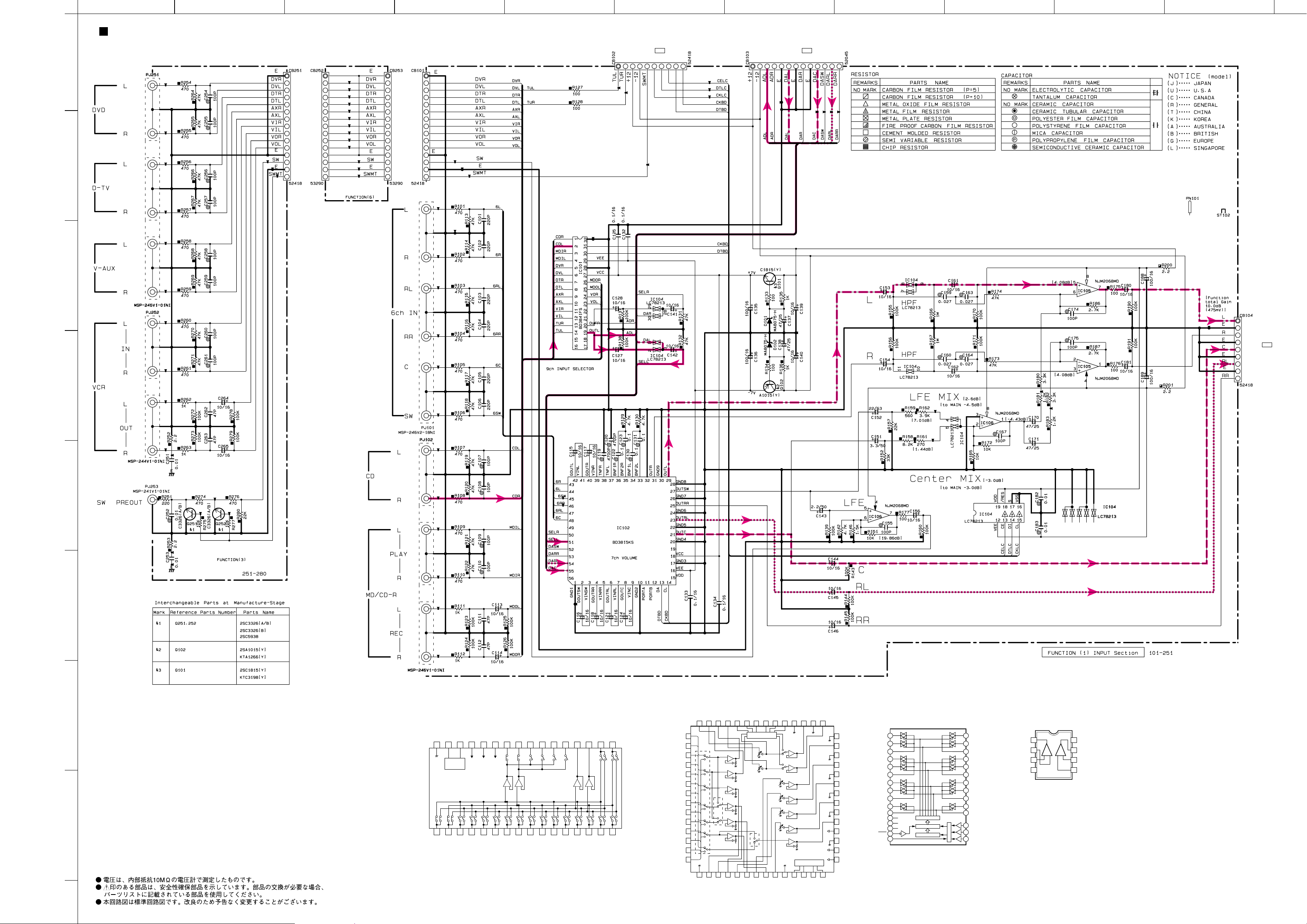
57
SCHEMATIC DIAGRAM (FUNCTION 1/2)
1
2
3
4
5
6
7
8
9
★ All voltages are measured with a 10MΩ/V DC electronic voltmeter.
★ Components having special characteristics are marked s and must be replaced
with parts having specifications equal to those originally installed.
★ Schematic diagram is subject to change without notice.
F-SW1
F-SW1: INPUT FUNCTION 1
F-SW2: INPUT FUNCTION 2
*
32 31 30 29 28 27 26 25 24 23 22 21 20 19 18 17
1 2 3 4 5 6 7 8 9 10 11 12 13 14 15 16
IC101: BD3841FS
Function Switch
DGND
F-SW2
CL
DA
VEE
BIAS
VCC
RECA1
RECA2
RECB1
RECB2
RECC1
RECC2
OUT1
OUT2
INI1
INI2
INA1
INA2
INB1
INB2
INC1
INC2
IND1
IND2
INE1
INE2
INF1
INF2
ING1
ING2
INH1
INH2
LOGIC
+
–
+
–
+
–
+
–
43
44
45
46
47
48
49
50
51
52
53
54
55
56
28
27
26
25
24
23
22
21
20
19
18
17
16
15
42 41 40 39 38 37 36 35 34 33 32 31 30 29
1 2 3 4 5 6 7 8 9 10 11 12 13 14
IC102: BD3815KS
Audio Sound Processor
GOUTFL
VINFL
GOUTFR
VINFR
TNFR
TNFL
BNF1R
BNF2R
BNF1L
BNF2L
GND10
OUTFR
GND9
OUTFL
GND8
OUTSW
GND7
OUTSR
GND6
OUTSL
GND5
OUTC
GND4
OUTSB
VCC
GND3
VEE
VDD
INFRA
INFLA
INSWA
INSRA
INSLA
INCA
INSBA
INFRB
INFLB
INSWB
INSRB
INSLB
INCB
INSBB
GND1
GOUTSW
VINSW
GOUTSR
INVINSR
GOUTSL
VINSL
GOUTC
VINC
GND2
PORTA
PORTB
DA
CL
TONE
A
SW1
B
A
B
LOGIC
A
B
A
B
A
B
A
B
A
B
A
B
A
B
+
–
+
–
+
–
+
–
+
–
+
–
+
–
SW2
A
B
SW3
+
–
+
–
+
–
+
–
+
–
+
–
IC104: LC78213
Analog Function Switch
1
2
3
4
5
6
7
8
9
10
11
30
29
28
27
26
25
24
23
22
21
20
19
16
12
18
17
14
15
13
LEVEL SHIFTER
LATCH
CONTROL
SHIFT REGISTER
ZZ
ZZ
ZZ
L1
L2
LCOM1
L3
L4
LCOM2
L5
LCOM3
L7
RES
S
V
DD
VSS
VEE
L6
LCOM4
R1
R2
RCOM1
R3
R4
R6
RCOM4
RCOM2
RCOM3
R7
D1
CL
CE
R5
IC105, 106: NJM2068MD
Dual OP-Amp.
–+
OUT1
–IN1
–VCC
+VCC
OUT2
1
2
3
4
5
+IN1 –IN2
+IN2
–+
6
7
8
0
0
7.0
7.7
7.7
0
0
0
0
0
0
0
0
0
0
0
0
0
0
0
0
0
0
-11.9
0
0
0
12.0
12.0
0
0
-11.9
0.2
6
12.0
0
12.0
-11.9
-7.0
0
12.0
0
-7.7
-7.7
-11.9
00
0
0
0
0
0
0
0
0
0
0
0
0
0
0
0
0
0
0
0
0
0
0
0
0
0
0
0
0
0
0
0
0
0
0
0
0
0
0
7.0
-7.0
0
0
0
0
0
0
0
0
0
0
0
0
0
0
0
0
0
0
0
0
0
0
0
0
0
0
0
0
0
-7.0
0
7.0
0
0
0
0
0
0
0
-11.8
0
0
-11.8
0
MUTE
AUDIO
SOUND
PROCESSOR
INPUT/
REC OUT
SELECTOR
Page 60
to MAIN (1)
E1 Page 56
to DSP
F1
Page 59
to MAIN (1)
A5
 Loading...