


 U BRACKET
UB-DXR8 / UB-DXR10 / UB-DXR12 / UB-DXR15
SERVICE MANUAL
• POWERED SPEAKER
DXR8/DXR10/DXR12/DXR15
DXR10 |
DXR12 |
DXR8 |
DXR15 |
• U BRACKET
UB-DXR8/UB-DXR10/UB-DXR12/UB-DXR15
UB-DXR15
UB-DXR12
UB-DXR10
UB-DXR8
CONTENTS |
|
SPECIFICATIONS .................................... |
3 |
PANEL LAYOUT ......................... |
4 |
CIRCUIT BOARD LAYOUT .... 5 |
|
DIMENSIONS ............................................... |
7 |
DISASSEMBLY PROCEDURE ................. |
8 |
LSI PIN DESCRIPTION LSI ................ |
26 |
CIRCUIT BOARDS .......................... |
27 |
TEST PROGRAM ..................... |
35 |
INSPECTIONS ............................................... |
45 |
UPDATING ...................................... |
55 |
PARTS LIST |
|
BLOCK DIAGRAM |
|
LEVEL DIAGRAM |
|
CIRCUIT DIAGRAM |
|
UB-DXR8/UB-DXR10/UB-DXR12/UB-DXR15 SERVICE MANUAL |
|
PA 012041
DXR8: |
201202-71400 |
UB-DXR8: 201202-10500 |
HAMAMATSU, JAPAN |
|||||
DXR10: |
201202-81900 |
UB-DXR10: 201202-10500 |
||||||
|
|
|
|
|
||||
DXR12: |
201202-92400 |
UB-DXR12: 201202-15750 |
Copyright (c)Yamaha Corporation. All rights reserved. PDF |
|
|
|
’12.03 |
|
|
|
|||||||
DXR15: |
201202-102900 |
UB-DXR15: 201202-15750 |
|
|
|
|
|
|
DXR8/DXR10/DXR12/DXR15
IMPORTANT NOTICE
This manual has been provided for the use of authorized Yamaha Retailers and their service personnel. It has been assumed that basic service procedures inherent to the industry, and more specifically Yamaha Products, are already known and understood by the users, and have therefore not been restated.
WARNING :
Failure to follow appropriate service and safety procedures when servicing this product may result in personal injury, destruction of expensive components and failure of the product to perform as specified. For these reasons, we advise
all Yamaha product owners that all service required should be performed by an authorized Yamaha Retailer or the appointed service representative.
IMPORTANT :
This presentation or sale of this manual to any individual or firm does not constitute authorization certification, recognition of any applicable technical capabilities, or establish a principal-agent relationship of any form.
The data provided is belived to be accurate and applicable to the unit(s) indicated on the cover. The research engineering, and service departments of Yamaha are continually striving to improve Yamaha products. Modifications are, therefore, inevitable and changes in specification are subject to change without notice or obligation to retrofit. Should any discrepancy appear to exist, please contact the distributor’s Service Division.
WARNING :
IMPORTANT :
Static discharges can destroy expensive components. Discharge any static electricity your body may have accumulated by grounding yourself to the ground bus in the unit (heavy gauge black wires connect to this bus.)
Turn the unit OFF during disassembly and parts replacement. Recheck all work before you apply power to the unit.
WARNING: This product contains chemicals known to the State of California to cause cancer, or birth defects or other reproductive harm.
DO NOT PLACE SOLDER, ELECTRICAL/ELECTRONIC OR PLASTIC COMPONENTS IN YOUR MOUTH FOR ANY REASON WHAT SO EVER!
Avoid prolonged, unprotected contact between solder and your skin! When soldering, do not inhale solder fumes or expose eyes to solder/ flux vapor!
If you come in contact with solder or components located inside the enclosure of this product, wash your hands before handling food.
IMPORTANT NOTICE FOR THE UNITED KINGDOM
Connecting the Plug and Cord
WARNING: THIS APPARATUS MUST BE EARTHED IMPORTANT.
The wires in this mains lead are coloured in accordance with the following code:
GREEN-AND-YELLOW : EARTH
BLUE |
: NEUTRAL |
BROWN |
: LIVE |
As the colours of the wires in the mains lead of this apparatus may not correspond with the coloured markings identifying the terminals in your plug proceed as follows:
The wire which is coloured GREEN-and-YELLOW must be connected to the terminal in the plug which is marked by the letter E or by the safety earth symbol  or colored GREEN or GREEN-and-YELLOW.
The wire which is coloured BLUE must be connected to the terminal which is marked with the letter N or coloured BLACK. The wire which is coloured BROWN must be connected to the terminal which is marked with the letter L or coloured RED.
(3 wires)
 WARNING
Components having special characteristics are marked  and must be replaced with parts having specification equal to those originally installed.

2
DXR8/DXR10/DXR12/DXR15
 SPECIFICATIONS
General |
DXR8 |
DXR10 |
DXR12 |
DXR15 |
|
|
|
|
|
System Type |
2-way, Bi-amp Powered Speaker, Bass-reflex Type |
|
|
|
|
|
|
|
|
Frequency Range (-10dB) |
57Hz – 20kHz |
56Hz – 20kHz |
52Hz – 20kHz |
49Hz – 20kHz |
Coverage Angle |
H90° x V60° Constant Directivity Horn |
|
|
|
|
|
|
|
|
Crossover Type |
FIR-X tuning™ (Linear Phase FIR Filter) |
|
|
|
Crossover Frequency |
2.4kHz |
2.3kHz |
2.1kHz |
2.1kHz |
|
|
|
|
|
Measured Maximum SPL (peak) |
129dB SPL |
131dB SPL |
132dB SPL |
133dB SPL |
IEC noise@1m |
|
|
|
|
|
Transducer |
DXR8 |
DXR10 |
DXR12 |
DXR15 |
||
|
|
|
|
|
|
|
|
LF |
|
Diameter |
8" Cone |
|
10" Cone |
12" Cone |
15" Cone |
|
|
Voice coil |
2" |
|
2" |
2.5" |
2.5" |
|
|
|
|
|
|
|
|
|
|
Magnet |
Ferrite |
|
|
|
|
HF |
|
Diaphragm |
1.4" |
|
|
|
|
|
|
|
|
|
|
|
|
|
|
Type |
1" Throat Compression Driver |
|
|
|
|
|
|
|
|
|
|
|
|
|
|
Magnet |
Ferrite |
|
|
|
|
Enclosure |
DXR8 |
DXR10 |
DXR12 |
DXR15 |
|
Material, Finish, Color |
ABS, Matte Black |
|
|
|
|
|
|
|
|
|
|
Floor Monitor Angle |
– |
50° |
50° Symmetrical |
|
50° Symmetrical |
|
|
|
|
|
|
Dimensions |
280×458×280 mm |
305×502×310 mm |
362×601×350 mm |
|
445×700×380 mm |
(WxHxD, with rubber feet) |
(11" x 18" x 11") |
(12" x 19-3/4" x 12-1/4") |
(14-1/4" x 23-5/8" x 13-3/4") |
|
(17-1/2" x 27-1/2" x 15") |
|
|
|
|
|
|
Net Weight |
13.5kg (29.8lbs) |
14.6kg (32.2lbs) |
19.3kg (42.5lbs) |
|
22.5kg (49.6lbs) |
|
|
|
|
|
|
Handles |
Aluminium die-cast (Top x 1) |
|
Aluminium die-cast (Side x 2) |
|
|
Pole Socket |
35mm with 2-way feature (0 or 7 degree) |
|
|
|
|
|
|
|
|||
Rigging points |
Top x 2, Rear x 1 (Fits for M8 x 15mm eyebolts) |
Top x 2, Rear x 1 (Fits for M10 x 18mm eyebolts) |
|||
|
|
|
|
|
|
Optional Accessory (U-bracket) |
UB-DXR8 |
UB-DXR10 |
UB-DXR12 |
|
UB-DXR15 |
Amplifier |
|
DXR8 |
DXR10 |
DXR12 |
DXR15 |
|
Amplifier Type |
|
Class-D |
|
|
|
|
|
|
|
|
|
|
|
Power Rating *1 |
Dynamic |
1100W (LF: 950W, HF: 150W) |
|
|
|
|
|
|
Continuous |
700W (LF: 600W, HF: 100W) |
|
|
|
Cooling |
|
Fan cooling, 4 speeds |
|
|
|
|
|
|
|
|
|
|
|
AD/DA |
|
24bit 48kHz sampling |
|
|
|
|
Signal Processing |
|
48bit (Accumulator: 76bit) |
|
|
|
|
|
|
|
|
|
|
|
HPF/LPF |
|
OFF, 100, 120Hz 24dB/oct HPF |
|
|
|
|
|
|
|
|
|
||
DSP preset |
|
D-CONTOUR: FOH/MAIN, MONITOR, OFF |
|
|
||
Protection |
Speaker |
Clip limiting, Integral Power Protection, DC-fault |
|
|
||
|
|
|
|
|
|
|
|
|
Amplifier |
Thermal, Output over current |
|
|
|
|
|
|
|
|
|
|
|
|
Power supply |
Thermal, Output over voltage, Output over current |
|
|
|
Connectors |
Input |
INPUT1: XLR3-31 x 1, INPUT2: Phone x 2 (Unbalanced), INPUT3: RCA PIN x 2 (Unbalanced) |
|
|||
|
|
|
|
|
|
|
|
|
Output |
THRU: XLR3-32 x 1 (Parallel with INPUT1), LINK OUT: XLR x1 |
|
||
Input Impedance |
INPUT1 |
LINE: 12kΩ, MIC: 8kΩ |
|
|
|
|
|
|
|
|
|
|
|
|
|
INPUT2, 3 |
L, R: 40kΩ, MONO: 20kΩ |
|
|
|
|
|
|
|
|
|
|
Input Sensitivity |
INPUT1 |
LINE: +1dBu, MIC: -32dBu |
|
|
|
|
(LEVEL: Maximum) |
|
INPUT2, 3 |
-13dBu |
|
|
|
|
|
|
|
|
||
|
|
|
|
|
|
|
Input Sensitivity |
INPUT1 |
LINE: +11dBu, MIC: -22dBu |
|
|
|
|
(LEVEL: Center) |
|
|
|
|
|
|
|
INPUT2, 3 |
-3dBu |
|
|
|
|
|
|
|
|
|
||
Maximum Input Level |
INPUT1 |
LINE: +24dBu, MIC: +20dBu |
|
|
|
|
|
|
|
|
|
|
|
|
|
INPUT2, 3 |
+16dBu |
|
|
|
Controls |
|
LEVEL x3, LINE/MIC, HPF, D-CONTOUR, FRONT LED DISABLE, LINK MODE, POWER |
|
|||
|
|
|
|
|
||
Idle Power Consumption |
35W |
|
|
|
||
|
|
|
|
|
||
1/8 Power Consumption |
90W |
|
110W |
|
||
Power Requirements |
|
100V – 240V, 50Hz/60Hz |
|
|
|
|
|
|
|
|
|
|
|
0dBu is referenced to 0.775Vrms. |
|
|
|
|
||
*1 Power rating (120V, 25°C). This is total value of individual output power. |
|
|
|
|||
• Included Accessories |
• |
· AC power cord |
· |
· Owner's manual |
· |
3
DXR8/DXR10/DXR12/DXR15
 PANEL LAYOUT
• Rear panel
|
|
• Tiltable pole socket
7˚
0˚
q [INPUT] jacks w [THRU] jack
e [LEVEL] control r [LIMIT] indicator t [SIGNAL] indicator
y [PROTECTION] indicator u [POWER] indicator
i [FRONT LED DISABLE] switch o [MIC/LINE] switch !0[D-CONTOUR] switch !1[HPF] switch
!2[LINK OUT] jack !3[LINK MODE] switch !4[AC IN] socket !5Power switch !6Tiltable pole socket
q [INPUT] w [THRU]
e [LEVEL] r [LIMIT] t [SIGNAL]
y [PROTECTION] u [POWER]
i [FRONT LED DISABLE] o [MIC/LINE]
!0[D-CONTOUR]
!1[HPF]
!2[LINK OUT]
!3[LINK MODE]
!4[AC IN]
!5
!6
4
DXR8/DXR10/DXR12/DXR15
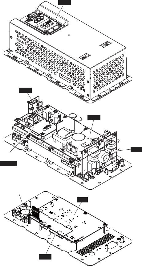
 CIRCUIT BOARD LAYOUT
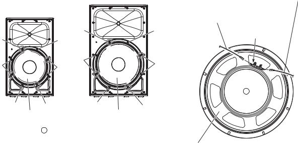
● DXR8 / DXR10
Front view ( ) |
Right side view ( ) |
Rear view ( ) |
|
SPEAKER (TWEETER) |
AMP ASSEMBLY |
||
|
Ass’y |
||
LED
SPEAKER (WOOFER)
This figure shows the DXR8.
DXR8
● DXR12 / DXR15
Front view ( ) |
Right side view ( ) |
Rear view ( ) |
|
SPEAKER (TWEETER) |
AMP ASSEMBLY |
||
|
Ass’y |
||
LED
SPEAKER (WOOFER) |
This figure shows the DXR12. |
|
DXR12 |
5
DXR8/DXR10/DXR12/DXR15
● AMP ASSEMBLY Ass’y
SUB3
SUB4
AMPS
SUB1
TWAMP ASSEMBLY
TWAMP Ass’y
TWAMP
DC FAN
DC
DSP
SUB2
6
|
|
|
|
|
DXR8/DXR10/DXR12/DXR15 |
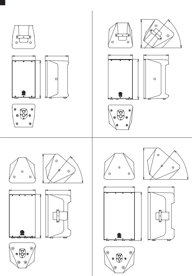
DIMENSIONS |
|
|
|
||
DXR8 |
|
|
DXR10 |
|
|
|
|
|
|
355 |
50° |
|
|
|
|
|
|
280 |
|
280 |
305 |
|
310 |
|
|
|
|
||
|
458 |
|
|
502 |
|
|
|
Unit : mm |
|
|
Unit : mm |
DXR12 |
|
|
DXR15 |
|
|
|
|
|
|
456 |
50° |
|
402 |
50° |
|
|
|
|
|
|
|
||
362 |
|
350 |
445 |
|
380 |
|
|
|
|
||
|
601 |
|
|
700 |
|
|
|
Unit : mm |
|
|
Unit : mm |
|
|
|
|
|
7 |
DXR8/DXR10/DXR12/DXR15
 DISASSEMBLY PROCEDURE
A. Disassembly of DXR8/DXR10
A-1. Metal Grille Assembly
(Time required: About 1 minute)
A-1-1 Remove the six (6) screws marked [150]. The metal grille assembly can then be removed. (Fig. A-1)
*When installing the metal grille assembly, first tighten the two (2) priority screws as shown in Fig. A-1.
A-2. Speaker (Woofer)
(Time required: About 3 minutes)
A-2-1 Remove the metal grille assembly. (See procedure A-1.) A-2-2 Remove the eight (8) screws marked [50]. The speaker
(woofer) can then be removed. (Fig. A-2, Fig. A-3)
*When installing the speaker (woofer), first tighten the four (4) priority screws in order as shown in Fig. A-3.
A-2-3 Remove the LFSPOUT connector assembly (red/black) attached to the speaker (woofer) terminal. (Fig. A-2, Fig. A-4)
*The speaker (woofer) is heavy. Be careful not to drop it.
[150]
PRIORITY SCREW
[150]
METAL GRILLE ASSEMBLY
Ass’y
PRIORITY SCREW |
This figure shows the DXR8. |
|
DXR8 |
A. DXR8/DXR10
A-1. Ass'y 1
A-1-1 [150] 6 Ass'y
A-1
Ass'y2 A-1
A-2. 3
A-2-1 Ass'y A-1
A-2-2 [50] 8 A-2 A-3
4 A-3
A-2-3
LFSPOUT
A-2 A-4
せない様に注意してください。
LFSPOUT CONNECTOR
ASSEMBLY (RED/BLACK)LFSPOUT /
SPEAKER (WOOFER)
This figure shows the DXR8.
[50]DXR8
Fig. A-1 A-1 |
Fig. A-2 A-2 |
8
DXR8/DXR10/DXR12/DXR15
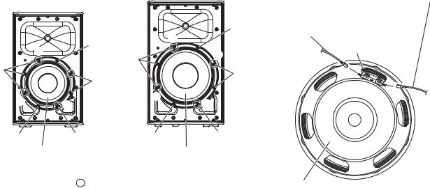
● DXR8
[50]
[50]
[50]
[50][50]
SPEAKER (WOOFER)
● DXR10
[50]
[50][50]
SPEAKER (WOOFER)
LFSPOUT CONNECTOR ASSEMBLY BLACK (–)
LFSPOUT
LFSPOUT CONNECTOR ASSEMBLY RED (+)
[50]LFSPOUT
RED MARKING
[50]
: PRIORITY SCREW |
SPEAKER (WOOFER) |
|
|
||
|
||
Fig. A-3 A-3 |
Fig. A-4 A-4 |
A-3. Baffle Assembly
(Time required: About 4 minutes)
A-3-1 Remove the metal grille assembly. (See procedure A-1.) A-3-2 DXR8:
Remove the twelve (12) screws marked [30A]. The baffle assembly can then be removed. (Fig. A-5, Fig. A-6)
DXR10:
Remove the fourteen (14) screws marked [30B]. The baffle assembly can then be removed. (Fig. A-5, Fig. A-6)
*DXR8:
When installing the baffle assembly, first tighten the four (4) priority screws as shown in Fig. A-6. DXR10:
When installing the baffle assembly, first tighten the six (6) priority screws in order as shown in Fig. A-6.
A-3-3 Disconnect the connectors of the LFSPOUT connector assembly (red/black), HFSPOUT connector assembly (yellow/blue) and C&C connector assembly (red/white) from the amp assembly. (Fig. A-5, Photo A-1)
*Take care not to open the baffle assembly too wide or these connector assemblies may be damaged. (Fig. A-5, Photo A-1)
A-3. Ass'y 4
A-3-1 Ass'y A-1 A-3-2 DXR8
[30A] 12 Ass'yA-5 A-6
DXR10
[30B] 14 Ass'yA-5 A-6
DXR8
Ass'y 4 A-6
DXR10
Ass'y 6A-6
A-3-3 Ass'y LFSPOUT HFSPOUT C&CA-5 A-1
Ass'y A-5 A-1
9
DXR8/DXR10/DXR12/DXR15
C & C CONNECTOR ASSEMBLY (RED/ WHITE)
C & C /
HFSPOUT CONNECTOR ASSEMBLY (YELLOW/BLUE)
HFSPOUT /
LFSPOUT CONNECTOR
ASSEMBLY (RED/BLACK)
LFSPOUT /
DXR8 : [30A] x 12 |
BAFFLE ASSEMBLY |
This figure shows the DXR8. |
DXR10 : [30B] x 14 |
Ass’y |
DXR8 |
|
Fig. A-5 A-5 |
|
● DXR8 |
● DXR10 |
|
[30A] |
BAFFLE ASSEMBLY |
[30B] |
Ass’y |
|
|
[30B]
[30A]
[30A]
[30A] |
: PRIORITY SCREW [30B] |
|
|
|
Fig. A-6 A-6 |
C & C CONNECTOR |
LFSPOUT CONNECTOR |
ASSEMBLY (RED) |
ASSEMBLY (RED) |
C & C |
LFSPOUT |
AMP ASSEMBLY
Ass’y
[30B]
LFSPOUT CONNECTOR ASSEMBLY (BLACK)LFSPOUT
HFSPOUT CONNECTOR ASSEMBLY (YELLOW)HFSPOUT
Photo A-1 A-1
10
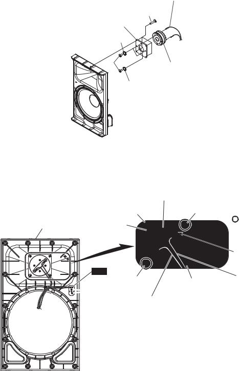
A-4. Speaker (Tweeter)
(Time required: About 5 minutes)
A-4-1 Remove the metal grille assembly. (See procedure A-1.) A-4-2 Remove the baffle assembly. (See procedure A-3.) A-4-3 Remove the HFSPOUT connector assembly (yellow/
blue) attached to the speaker (tweeter) terminal. (Fig. A-7, Fig. A-8)
A-4-4 Remove the four (4) screws marked [90]. The TW plate can then be removed together with the speaker (tweeter). (Fig. A-7, Fig. A-8)
*When installing the TW plate, first tighten the two (2) priority screws as shown in Fig. A-8.
A-4-5 Remove the four (4) screws marked [80] and four
(4) toothed lock washers marked [280]. The speaker (tweeter) can then be removed from the TW plate. (Fig. A-7)
A-5. LED Circuit Board
(Time required: About 4 minutes)
A-5-1 Remove the metal grille assembly. (See procedure A-1.) A-5-2 Remove the baffle assembly. (See procedure A-3.) A-5-3 Remove the two (2) screws marked [170]. The LED
circuit board can then be removed. (Fig. A-8, Fig. A-9)
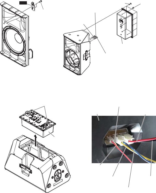
A-6. Amp Assembly
(Time required: About 3 minutes)
A-6-1 Remove the twelve (12) screws marked [50]. (Fig. A-10)
*When installing the amp assembly, first tighten the priority screw as shown in Fig. A-10.
A-6-2 Loosen the two (2) screws for removing the amp assembly. (Fig. A-11)
*Loosen only ! Never remove these screws. Tighten these screws when installing the amp assembly. (Fig. A-11)
A-6-3 Hold the two (2) screws for removing the amp assembly and then remove the amp assembly carefully. (Fig. A-11)
A-6-4 Disconnect the connectors of the LFSPOUT connector assembly (red/black), HFSPOUT connector assembly (yellow/blue) and C&C connector assembly (red/white) from the amp assembly. (Fig. A-10, Photo A-2)
*Take care not to pull the amp assembly too wide or these connector assemblies may be damaged. (Fig. A-10, Photo A-2)
For about disassembly of amp assembly, refer to 20 page.
DXR8/DXR10/DXR12/DXR15
A-4. 5
A-4-1 Ass'y A-1 A-4-2 Ass'y A-3
A-4-3
HFSPOUT
A-7 A-8
A-4-4 [90] 4TW A-7 A-8
TW 2A-8
A-4-5 [80] 4 [280] 4TW A-7
A-5. LED 4
A-5-1 Ass'y A-1 A-5-2 Ass'y A-3
A-5-3 [170] 2 LED
A-8 A-9
A-6. Ass'y 3
A-6-1 [50] 12 A-10
Ass'y 1A-10
A-6-2 Ass'y 2
A-11
ください。アンプAss'yA-11
A-6-3 Ass'y 2Ass'y A-11
A-6-4 Ass'y LFSPOUT HFSPOUT C&CA-10 A-2
Ass'y A-10 A-2
Ass'y 20
11
DXR8/DXR10/DXR12/DXR15
HFSPOUT CONNECTOR ASSEMBLY (YELLOW/BLUE)
HFSPOUT /
[90]
TW PLATE
TW
[280]
[80]
SPEAKER (TWEETER)
[280]
This figure shows the DXR8.
DXR8
Fig. A-7 A-7
SPEAKER (TWEETER)
[90] [90]
BAFFLE ASSEMBLY
Ass’y TW PLATE TW
LED |
|
|
[170] |
[90] |
[90] |
|
||
|
|
|
|
HFSPOUT CONNECTOR |
|
|
ASSEMBLY BLUE (–) |
|
|
HFSPOUT |
|
This figure shows the DXR8.
DXR8
Fig. A-8 A-8
: PRIORITY SCREW
RED MARKING
HFSPOUT CONNECTOR ASSEMBLY YELLOW (+)HFSPOUT
12
DXR8/DXR10/DXR12/DXR15
LED |
|
HFSPOUT CONNECTOR |
[50] |
|
|
ASSEMBLY (YELLOW/BLUE) |
|
|
[170] |
HFSPOUT / |
|
|
|
|
C & C CONNECTOR ASSEMBLY (RED/ WHITE)
C & C /
PRIORITY SCREW
This figure shows the DXR8.
DXR8
Fig. A-9 A-9
SCREW FOR REMOVING THE AMP ASSEMBLY
Ass’y
AMP ASSEMBLY
Ass’y
This figure shows the DXR8.
DXR8
Fig. A-11 A-11
AMP ASSEMBLY
Ass’y
LFSPOUT CONNECTOR ASSEMBLY (RED/BLACK)
LFSPOUT /
This figure shows the DXR8.
DXR8
Fig. A-10 A-10
C & C CONNECTOR ASSEMBLY (WHITE)C & C
AMP ASSEMBLY
Ass’y
C & C CONNECTOR
ASSEMBLY (RED)
C & C
HFSPOUT CONNECTOR ASSEMBLY (YELLOW)HFSPOUT
HFSPOUT CONNECTOR ASSEMBLY (BLUE)HFSPOUT
Photo A-2 A-2
13
DXR8/DXR10/DXR12/DXR15
B. |
Disassembly of DXR12/DXR15 |
B. |
DXR12/DXR15 |
B-1. |
Metal Grille Assembly |
B-1. |
Ass'y 1 |
|
(Time required: About 1 minute) |
B-1-1 [150] 8 Ass'y |
|
B-1-1 |
Remove the eight (8) screws marked [150]. The metal |
|
B-1 |
|
grille assembly can then be removed. (Fig. B-1) |
|
Ass'y |
* |
When installing the metal grille assembly, first |
|
4 B-1 |
|
tighten the four (4) priority screws as shown in |
|
|
|
Fig. B-1. |
|
|
B-2. Speaker (Woofer)
(Time required: About 3 minutes)
B-2-1 Remove the metal grille assembly. (See procedure B-1.) B-2-2 Remove the eight (8) screws marked [50]. The speaker
(woofer) can then be removed. (Fig. B-2, Fig. B-3)
*When installing the speaker (woofer), first tighten the four (4) priority screws in order as shown in Fig. B-3.
B-2-3 Remove the LFSPOUT connector assembly (red/black) attached to the speaker (woofer) terminal.
(Fig. B-2, Fig. B-4)
*The speaker (woofer) is heavy. Be careful not to drop it.
[150]
PRIORITY SCREW
[150]
PRIORITY SCREW
METAL GRILLE ASSEMBLY
Ass’y
This figure shows the DXR12.
DXR12
Fig. B-1 B-1
B-2. 3
B-2-1 Ass'y B-1
B-2-2 [50] 8 B-2 B-3
4 B-3
B-2-3
LFSPOUT
B-2 B-4
せない様に注意してください。
LFSPOUT CONNECTOR ASSEMBLY (RED/BLACK)
LFSPOUT /
SPEAKER (WOOFER)
[50] |
This figure shows the DXR12. |
|
DXR12 |
||
|
||
|
Fig. B-2 B-2 |
14
DXR8/DXR10/DXR12/DXR15
● DXR12 |
● DXR15 |
|
LFSPOUT CONNECTOR ASSEMBLY BLACK (–) |
|
|
|
LFSPOUT |
|
|
|
LFSPOUT CONNECTOR ASSEMBLY RED (+) |
|
|
|
LFSPOUT |
|
[50] |
[50] |
RED MARKING |
|
|
||
[50] |
[50] |
|
|
|
|
||
[50] |
[50] |
[50] |
|
[50] |
|
||
|
|
|
[50] |
[50] |
[50] |
[50] |
|
|
|
|
|
|
SPEAKER (WOOFER) |
SPEAKER (WOOFER) |
|
||
|
|
|
||
|
: PRIORITY SCREW |
|
|
|
|
|
|
|
|
|
Fig. B-3 B-3 |
|
SPEAKER (WOOFER) |
|
Fig. B-4 B-4
B-3. Baffle Assembly
(Time required: About 4 minutes)
B-3-1 Remove the metal grille assembly. (See procedure B-1.) B-3-2 DXR12:
Remove the fourteen (14) screws marked [30A]. The baffle assembly can then be removed. (Fig. B-5, Fig. B-6)
DXR15:
Remove the sixteen (16) screws marked [30B]. The baffle assembly can then be removed. (Fig. B-5, Fig. B-6)
*DXR12:
When installing the baffle assembly, first tighten the six (6) priority screws in order as shown in Fig. B-6. DXR15:
When installing the baffle assembly, first tighten the four (4) priority screws as shown in Fig. B-6.
B-3-3 Disconnect the connectors of the LFSPOUT connector assembly (red/black), HFSPOUT connector assembly (yellow/blue) and C&C connector assembly (red/white) from the amp assembly. (Fig. B-5, Photo B-1)
*Take care not to open the baffle assembly too wide or these connector assemblies may be damaged. (Fig. B-5, Photo B-1)
B-3. Ass'y 4
B-3-1 Ass'y B-1 B-3-2 DXR12
[30A] 14 Ass'yB-5 B-6
DXR15
[30B] 16 Ass'yB-5 B-6
DXR12
Ass'y 6B-6 DXR15
Ass'y 4 B-6
B-3-3 Ass'y LFSPOUT HFSPOUT C&CB-5 B-1
Ass'y B-5 B-1
15
DXR8/DXR10/DXR12/DXR15
C & C CONNECTOR
ASSEMBLY (RED/ WHITE)
C & C /
HFSPOUT CONNECTOR
ASSEMBLY (YELLOW/BLUE)
HFSPOUT /
|
LFSPOUT CONNECTOR |
|
ASSEMBLY (RED/BLACK) |
|
LFSPOUT / |
|
BAFFLE ASSEMBLY |
|
Ass’y |
DXR12 : [30A] x 14 |
This figure shows the DXR12. |
DXR15 : [30B] x 16 |
DXR12 |
|
Fig. B-5 B-5 |
● DXR12 |
● DXR15 |
[30B]
BAFFLE ASSEMBLY
[30A] Ass’y
[30B]
[30A] |
[30A] |
[30B]
[30A] |
[30B] |
|
: PRIORITY SCREW |
|
|
|
Fig. B-6 B-6 |
C & C CONNECTOR |
LFSPOUT CONNECTOR |
ASSEMBLY (RED) |
ASSEMBLY (RED) |
C & C |
LFSPOUT |
AMP ASSEMBLY
Ass’y
[30B]
[30B]
C & C CONNECTOR |
|
ASSEMBLY (WHITE) |
LFSPOUT CONNECTOR |
C & C |
ASSEMBLY (BLACK) |
HFSPOUT CONNECTOR |
LFSPOUT |
|
|
||
ASSEMBLY (BLUE) |
|
HFSPOUT CONNECTOR |
|
|
|
HFSPOUT ASSEMBLY (YELLOW) |
||
|
HFSPOUT |
|
Photo B-1 B-1
16
B-4. Speaker (Tweeter)
(Time required: About 5 minutes)
B-4-1 Remove the metal grille assembly. (See procedure B-1.) B-4-2 Remove the baffle assembly. (See procedure B-3.) B-4-3 Remove the HFSPOUT connector assembly (yellow/
blue) attached to the speaker (tweeter) terminal. (Fig. B-7, Fig. B-8)
B-4-4 Remove the four (4) screws marked [90]. The TW plate can then be removed together with the speaker (tweeter). (Fig. B-7, Fig. B-8)
*When installing the TW plate, first tighten the two (2) priority screws as shown in Fig. B-8.
B-4-5 Remove the four (4) screws marked [80] and four
(4) toothed lock washers marked [280]. The speaker (tweeter) can then be removed from the TW plate. (Fig. B-7)
B-5. LED Circuit Board
(Time required: About 4 minutes)
B-5-1 Remove the metal grille assembly. (See procedure B-1.) B-5-2 Remove the baffle assembly. (See procedure B-3.) B-5-3 Remove the two (2) screws marked [170]. The LED
circuit board can then be removed. (Fig. B-8, Fig. B-9)
B-6. Amp Assembly
(Time required: About 6 minutes)
B-6-1 Remove the metal grille assembly. (See procedure B-1.) B-6-2 Remove the speaker (woofer). (See procedure B-2.) B-6-3 Disconnect the connectors of the LFSPOUT connector
assembly (red/black), HFSPOUT connector assembly (yellow/blue) and C&C connector assembly (red/white) from the amp assembly. (Fig. B-10, Photo B-2)
B-6-4 Remove the twelve (12) screws marked [130]. (Fig. B-10)
*When installing the amp assembly, first tighten the priority screw as shown in Fig. B-10.
B-6-5 Loosen the two (2) screws for removing the amp assembly. (Fig. B-11)
*Loosen only ! Never remove these screws. Tighten these screws when installing the amp assembly. (Fig. B-11)
B-6-6 Hold the two (2) screws for removing the amp assembly and then remove the amp assembly carefully. (Fig. B-11)
For about disassembly of amp assembly, refer to 20 page.
DXR8/DXR10/DXR12/DXR15
B-4. 5
B-4-1 Ass'y B-1 B-4-2 Ass'y B-3
B-4-3
HFSPOUT
B-7 B-8
B-4-4 [90] 4TW B-7 B-8
TW 2B-8
B-4-5 [80] 4 [280] 4TW B-7
B-5. LED 4
B-5-1 Ass'y B-1 B-5-2 Ass'y B-3
B-5-3 [170] 2 LED
B-8 B-9
B-6. Ass'y 6
B-6-1 Ass'y B-1
B-6-2 B-2
B-6-3 Ass'y LFSPOUT HFSPOUT C&CB-10 B-2
B-6-4 [130] 12 B-10
Ass'y 1B-10
B-6-5 Ass'y 2
B-11
ください。アンプAss'yB-11
B-6-6 Ass'y 2Ass'y B-11
Ass'y 20
17
DXR8/DXR10/DXR12/DXR15
HFSPOUT CONNECTOR ASSEMBLY (YELLOW/BLUE)
HFSPOUT /
[90]
TW PLATE
TW
[280]
[80]
SPEAKER (TWEETER)
[280]
This figure shows the DXR12.
DXR12
Fig. B-7 B-7
SPEAKER (TWEETER)
[90] |
[90] |
BAFFLE ASSEMBLY
Ass’y TW PLATE TW
LED
[90] |
[90] |
|
 [170]
[170]
HFSPOUT CONNECTOR
ASSEMBLY BLUE (–)
HFSPOUT
This figure shows the DXR12.
DXR12
Fig. B-8 B-8
: PRIORITY SCREW
RED MARKING
HFSPOUT CONNECTOR ASSEMBLY YELLOW (+)
HFSPOUT
18
DXR8/DXR10/DXR12/DXR15
LED |
HFSPOUT CONNECTOR |
[130] |
PRIORITY SCREW |
|
ASSEMBLY (YELLOW/BLUE) |
|
|
|
|
|
|
|
|
|
[170]HFSPOUT /
C & C CONNECTOR ASSEMBLY (RED/ WHITE)
C & C /
|
AMP ASSEMBLY |
|
Ass’y |
|
LFSPOUT CONNECTOR |
|
ASSEMBLY (RED/BLACK) |
|
LFSPOUT / |
This figure shows the DXR12. |
This figure shows the DXR12. |
DXR12 |
DXR12 |
Fig. B-9 B-9 |
Fig. B-10 B-10 |
|
SCREW FOR REMOVING THE AMP ASSEMBLY |
C & C CONNECTOR ASSEMBLY (WHITE) |
||
Ass’y |
|||
C & C |
LFSPOUT CONNECTOR |
||
|
|||
|
AMP ASSEMBLY |
||
|
ASSEMBLY (RED) |
||
|
Ass’y |
LFSPOUT |
|
AMP ASSEMBLY
Ass’y
C & C CONNECTOR
ASSEMBLY (RED)
C & C
HFSPOUT CONNECTOR ASSEMBLY (YELLOW)HFSPOUT
HFSPOUT CONNECTOR ASSEMBLY (BLUE)
This figure shows the DXR12. HFSPOUT
DXR12
Photo B-2 B-2
Fig. B-11 B-11
19

DXR8/DXR10/DXR12/DXR15
C.Disassembly of Amp Assembly
*Before disassembly, remove the amp assembly in advance. (See procedure A-6, B-6.)
C-1. Amp Cover Assembly
(Time required: About 2 minutes)
C-1-1 Remove the twelve (12) screws marked [540]. The amp cover assembly can then be removed. (Fig. C-1)
C-2. SUB3 Circuit Board
(Time required: About 3 minutes)
C-2-1 Remove the amp cover assembly. (See procedure C-1.) C-2-2 Remove the four (4) screws marked [500]. The SUB3 circuit board can then be removed. (Fig. C-2)
*The cushion OUT is not part of the SUB3 circuit board. When replacing the SUB3 circuit board, remove the cushion OUT from the SUB3 circuit board and install it to the new circuit board. (Fig. C-2)
AMP COVER ASSEMBLY
Ass’y
[540]
Fig. C-1 C-1
C-3. Shield Assembly
(Time required: About 4 minutes)
C-3-1 Remove the amp cover assembly. (See procedure C-1.) C-3-2 Remove the SUB3 circuit board. (See procedure C-2.) C-3-3 Remove the three (3) screws marked [510] and two (2) screws marked [520]. The shield assembly can then be
removed. (Fig. C-3)
C.Ass'y
Ass'y
A-6 B-6
C-1. Ass'y 2
C-1-1 [540] 12 Ass'y
C-1
C-2. SUB3 3
C-2-1 Ass'y C-1
C-2-2 [500] 4 SUB3C-2
OUT SUB3SUB3 SUB3OUT C-2
&86+,21 287
> @
OUT
68%
Fig. C-2 C-2
C-3. Ass'y 4
C-3-1 Ass'y C-1 C-3-2 SUB3 C-2
C-3-3 [510] 3 [520] 2Ass'y C-3
20
DXR8/DXR10/DXR12/DXR15
[510]
[510]
[520]
SHIELD ASSEMBLY
Ass’y
Fig. C-3 C-3
C-4. TWAMP Assembly
(Time required: About 5 minutes)
C-4-1 Remove the amp cover assembly. (See procedure C-1.) C-4-2 Remove the SUB3 circuit board. (See procedure C-2.) C-4-3 Remove the shield assembly. (See procedure C-3.)
C-4-4 Remove the four (4) screws marked [320]. The TWAMP assembly can then be removed. (Fig. C-4)
*When installing the TWAMP assembly, first tighten the two (2) priority screws in order as shown in Fig. C-4.
C-5. AMPS Circuit Board
(Time required: About 7 minutes)
C-5-1 Remove the amp cover assembly. (See procedure C-1.) C-5-2 Remove the SUB3 circuit board. (See procedure C-2.) C-5-3 Remove the shield assembly. (See procedure C-3.)
C-5-4 Remove the TWAMP assembly. (See procedure C-4.) C-5-5 Remove the ten (10) screws marked [220] and four (4)
hexagonal spacers marked [310]. The AMPS circuit board can then be removed. (Fig. C-4)
*When installing the AMPS circuit board, first tighten the two (2) priority screws in order as shown in
Fig. C-4.
C-4. TWAMP Ass'y 5
C-4-1 Ass'y C-1 C-4-2 SUB3 C-2
C-4-3 Ass'y C-3
C-4-4 [320] 4 TWAMP Ass'yC-4
TWAMP Ass'y 2C-4
C-5. AMPS 7
C-5-1 Ass'y C-1 C-5-2 SUB3 C-2
C-5-3 Ass'y C-3 C-5-4 TWAMP Ass'y C-4
C-5-5 [220] 10 [310] 4AMPS C-4
AMPS 2C-4
21
DXR8/DXR10/DXR12/DXR15
C-6. |
SUB4 Circuit Board |
C-6. SUB4 4 |
|
|
(Time required: About 4 minutes) |
C-6-1 |
Ass'y C-1 |
C-6-1 |
Remove the amp cover assembly. (See procedure C-1.) |
C-6-2 |
SUB3 C-2 |
C-6-2 |
Remove the SUB3 circuit board. (See procedure C-2.) |
C-6-3 |
Ass'y C-3 |
C-6-3 |
Remove the shield assembly. (See procedure C-3.) |
C-6-4 |
[370] 1 SUB4 |
C-6-4 |
Remove the screw marked [370]. The SUB4 circuit |
|
C-4 |
|
board can then be removed. (Fig. C-4) |
|
|
> @
> @
35,25,7< 6&5(: w |
7:$03$66(0%/< (TWAMP Ass’y) |
|
|
w |
35,25,7< 6&5(: q q |
|
|
> @ |
|
> @ |
35,25,7< 6&5(: q q |
|
> @ |
|
35,25,7< 6&5(: w w |
|
68% |
|
$036 |
|
> @ |
Fig. C-4 C-4
C-7. SUB1 Circuit Board
(Time required: About 6 minutes)
C-7-1 Remove the amp cover assembly. (See procedure C-1.) C-7-2 Remove the SUB3 circuit board. (See procedure C-2.) C-7-3 Remove the shield assembly. (See procedure C-3.)
C-7-4 Remove the two (2) screws marked [70], three (3) screws marked [80] and the screw marked [90]. The shield ACIN can then be removed together with the SUB1 circuit board. (Fig. C-5)
*When installing the shield ACIN, first tighten the two
(2) priority screws in order as shown in Fig. C-5.
*When installing the screw marked [90], tighten so that the terminal lug points within the 90-degree range as shown in Fig. C-5.
C-7. SUB1 6
C-7-1 Ass'y C-1 C-7-2 SUB3 C-2
C-7-3 Ass'y C-3
C-7-4 [70] 2 [80] 3 [90] 1
SUB1 ACINC-5
ACIN 2
C-5
[90] 90
C-5
22
DXR8/DXR10/DXR12/DXR15
C-7-5 Remove the four (4) screws marked [50] and two (2) screws marked [60]. The SUB1 circuit board can then be removed from the shield ACIN. (Fig. C-5)
*When installing the SUB1 circuit board, first tighten the two (2) priority screws as shown in Fig. C-5.
C-7-6 Remove the power knob from the SUB1 circuit board. (Fig. C-5)
C-7-7 Straighten the two claws of the inlet angle and remove the inlet angle from the SUB1 circuit board. (Fig. C-5, Photo C-1)
*The power knob and the inlet angle are not parts of the SUB1 circuit board. When replacing the SUB1 circuit board, remove the power knob and the inlet angle from the SUB1 circuit board and install them to the new circuit board. (Fig. C-5)
C-7-5 [50] 4 [60] 2
ACIN SUB1
C-5
SUB1 2C-5
C-7-6 SUB1 C-5 C-7-7 2SUB1
C-5 C-1
SUB1SUB1 SUB1 C-5
SUB1
CLAW
Photo C-1 C-1
|
|
|
SUB1 |
SHIELD ACIN |
|
|
[50] |
|
|
|
|
ACIN |
|
|
|
|
|
|
PRIORITY SCREW |
PRIORITY SCREW |
|
|
CLAW |
[60] |
|
|
|
|
|
||
|
|
||
POWER KNOB |
|
INLET ANGLE |
|
|
|
||
|
|
||
|
|
|
|
|
|
[90] |
90-degree |
|
|
|
|
|
|
|
90 |
[90]
[70] |
|
PRIORITY SCREW |
|
|
TERMINAL LUG |
[80] PRIORITY SCREW |
|
|
|
Fig. C-5 C-5 |
|
23
DXR8/DXR10/DXR12/DXR15
C-8. DSP Circuit Board, SUB2 Circuit Board
(Time required: About 9 minutes)
C-8-1 Remove the amp cover assembly. (See procedure C-1.) C-8-2 Remove the SUB3 circuit board. (See procedure C-2.) C-8-3 Remove the shield assembly. (See procedure C-3.)
C-8-4 Remove the six (6) screws marked [150] from the rear panel side. The shield DSP assembly can then be removed together with the AMPS circuit board,
TWAMP assembly and SUB4 circuit board. (Fig. C-6)
*When installing the shield DSP assembly, first tighten the two (2) priority screws in order as shown in Fig. C-6.
C-8-5 Remove the three (3) volume knobs (black), seven (7) screws marked [160], two (2) hexagonal nuts marked [A] and two (2) flat washers marked [B] from the rear panel side. (Fig. C-7)
C-8-6 Remove the six (6) screws marked [130]. The DSP circuit board can then be removed together with the SUB2 circuit board. (Fig. C-6)
C-8-7 Remove the SUB2 circuit board from the six (6) locking card spacers of the DSP circuit board. (Fig. C-6)
*The push button HPF, the button joint HPF and the six (6) locking card spacers are not parts of the DSP circuit board. When replacing the DSP circuit board, remove the push button HPF, the button joint HPF and the six (6) locking card spacers from the DSP circuit board and install them to the new circuit board. (Fig. C-6, Fig. C-7)
*The push button HPF and the six (6) ring cushions are not parts of the SUB2 circuit board. When replacing the SUB2 circuit board, remove the push button HPF and the six (6) ring cushions from the SUB2 circuit board and install them to the new circuit board. (Fig. C-6, Fig. C-7)
C-9. DC Fan
(Time required: About 5 minutes)
C-9-1 Remove the amp cover assembly. (See procedure C-1.) C-9-2 Remove the SUB3 circuit board. (See procedure C-2.) C-9-3 Remove the shield assembly. (See procedure C-3.)
C-9-4 Remove the four (4) screws marked [410] and four (4) hexagonal flange nuts marked [420]. The DC fan can then be removed. (Fig. C-6)
C-8. DSP SUB2 9
C-8-1 Ass'y C-1 C-8-2 SUB3 C-2
C-8-3 Ass'y C-3
C-8-4 [150] 6
AMPS TWAMP Ass'y SUB4DSP Ass'y C-6
DSP Ass'y 2C-6
C-8-5 VR 3 [160]7 [A] 2 [B] 2 C-7
C-8-6 [130] 6 SUB2
DSP C-6
C-8-7 DSP 6
SUB2 C-6
HPF 1 HPF 16 DSPDSP DSPHPF 1 HPF 16 C-6 C-7
HPF 1 6 SUB2SUB2SUB2 HPF 16 C-6 C-7
C-9. DC 5
C-9-1 Ass'y C-1 C-9-2 SUB3 C-2
C-9-3 Ass'y C-3
C-9-4 [410] 4 [420] 4
DC C-6
24
DXR8/DXR10/DXR12/DXR15
SUB4 |
AMPS |
TWAMP ASSEMBLY
TWAMP Ass’y
LOCKING CARD SPACER |
|
|
|
|
|
|
|
SHIELD DSP ASSEMBLY |
|
[130] |
DSP Ass’y |
|
|
|
|
|
[130] |
RING CUSHION |
|
|
|
|
|
|
[420] |
|
|
|
DSP |
|
|
RING CUSHION |
|
SUB2 |
|
DC FAN |
|
|
|
|
|
DC |
|
|
|
|
REAR PANEL |
|
[410] |
|
|
PRIORITY SCREW |
|
|
|
[150] |
|
|
|
|
|
PRIORITY SCREW |
|
|
|
|
|
Fig. C-6 C-6 |
|
VOLUME KNOB |
PUSH BUTTON HPF |
|
(BLACK) |
HPF |
|
VR |
|
[A] |
PUSH BUTTON HPF |
|
[160]HPF
[B]BUTTON JOINT HPF
HPF
REAR PANEL
Fig. C-7 C-7
25
DXR8/DXR10/DXR12/DXR15
 LSI PIN DESCRIPTIONLSI
PCM1804DBR (X6872A00) ADC (Analog to Digital Converter) .......................................................... |
26 |
R5F212BCSNFP (YE165C00) MCU (Micro Controller Unit)................................................................ |
26 |
TAS3204PAGR (YA768A00) DSP (Digital Signal Processor) .............................................................. |
27 |
PCM1804DBR (X6872A00) ADC (Analog to Digital Converter) |
DSP: IC703 |
|||||||||||
PIN |
|
NAME |
I/O |
FUNCTION |
PIN |
NAME |
I/O |
|
FUNCTION |
|||
NO. |
|
NO. |
|
|||||||||
|
|
|
|
|
|
|
|
|
|
|
||
1 |
|
VREFL |
- |
L-channel voltage reference output, |
16 |
BCK/DSDL |
I/O |
|
Bit clock input/output in PCM mode / |
|||
|
|
|
|
|
requires capacitors for decoupling to AGND |
|
|
|
|
|
|
L-channel audio data output in DSD mode |
2 |
|
AGNDL |
- |
Analog ground for VREFL |
17 |
LRCK/DSDBCK |
I/O |
|
Sampling clock input/output in PCM and |
|||
3 |
|
VCOML |
- |
L-channel analog common-mode voltage (2.5 V) |
|
|
|
|
|
|
DSD modes |
|
4 |
|
VINL+ |
I |
L-channel analog input, positive pin |
18 |
SCKI |
I |
|
System clock input |
|||
5 |
|
VINL– |
I |
L-channel analog input, negative pin |
19 |
RST |
I |
|
Reset, power-down input, active-low |
|||
6 |
|
FMT0 |
I |
Audio data format 0 |
20 |
OVFR |
O |
|
Overflow signal of R-channel in PCM mode |
|||
7 |
|
FMT1 |
I |
Audio data format 1 |
21 |
OVFL |
O |
|
Overflow signal of L-channel in PCM mode |
|||
8 |
|
S/M |
I |
Slave/master mode selection |
22 |
VCC |
- |
|
|
Analog power supply +5 V |
||
9 |
|
OSR0 |
I |
Oversampling ratio 0 |
23 |
AGND |
- |
|
|
Analog ground |
||
10 |
|
OSR1 |
I |
Oversampling ratio 1 |
24 |
VINR– |
I |
|
R-channel analog input, negative pin |
|||
11 |
|
OSR2 |
I |
Oversampling ratio 2 |
25 |
VINR+ |
I |
|
R-channel analog input, positive pin |
|||
12 |
|
BYPAS |
I |
HPF bypass control |
26 |
VCOMR |
- |
|
|
R-channel analog common-mode voltage (2.5 V) |
||
13 |
|
DGND |
- |
Digital ground |
27 |
AGNDR |
- |
|
|
Analog ground for VREFR |
||
14 |
|
VDD |
- |
Digital power supply +3.3 V |
28 |
VREFR |
- |
|
|
R-channel voltage reference output, |
||
15 |
DATA/DSDR |
O |
L-channel and R-channel audio data output in PCM |
|
|
|
|
|
|
requires capacitors for decoupling to AGND |
||
|
|
|
|
|
mode / R-channel audio data output in DSD mode |
|
|
|
|
|
|
|
R5F212BCSNFP (YE165C00) MCU (Micro Controller Unit) |
DSP: IC701 |
|||||||||||
|
|
|
|
|
|
|
|
|
|
|
|
|
PIN |
|
NAME |
I/O |
FUNCTION |
PIN |
NAME |
|
I/O |
|
|
FUNCTION |
|
NO. |
|
NO. |
|
|
||||||||
|
|
|
|
|
|
|
|
|
|
|
||
|
|
|
|
|
|
|
|
|
|
|
|
|
1 |
P3_3/SSI |
I/O |
I/O port / Data I/O |
33 |
P8_1/TRFO01 |
|
I/O |
|
I/O port / Timer RF output |
|||
2 |
P3_4/SDA/SCS |
I/O |
I/O port / Data I/O / Chip-select signal I/O |
34 |
P8_0/TRFO00 |
|
I/O |
|
|
|||
|
|
|
||||||||||
3 |
|
MODE |
I |
Connect this pin to VCC via a resistor. |
35 |
P6_0/TREO |
|
I/O |
|
I/O port / Divided clock output |
||
4 |
P4_3/XCIN |
I/O |
I/O port / XCIN clock input |
36 |
P4_5/INT0 |
|
I/O |
|
I/O port / INT interrupt input |
|||
5 |
P4_4/XCOUT |
I/O |
I/O port / XCIN clock output |
37 |
P6_6/INT2/TXD1 |
|
I/O |
|
I/O port / INT interrupt input / Serial data output |
|||
6 |
|
RESET |
|
I |
Input “L” on this pin resets the MCU. |
38 |
P6_7/INT3/RXD1 |
|
I/O |
|
|
I/O port / INT interrupt input / Serial data input |
7 |
P4_7/XOUT |
I/O |
Input port / XIN clock output |
39 |
P6_5/(CLK1)/CLK2 |
|
I/O |
|
I/O port / (Transfer clock I/O) / Transfer clock I/O |
|||
8 |
VSS/AVSS |
- |
Ground |
40 |
P6_4/RXD2 |
|
I/O |
|
I/O port / Serial data input |
|||
9 |
P4_6/XIN |
I |
Input port / XIN clock input |
41 |
P6_3/TXD2 |
|
I/O |
|
I/O port / Serial data output |
|||
10 |
VCC/AVCC |
- |
Power supply +3.3 V |
42 |
P3_1/TRBO |
|
I/O |
|
I/O port / Timer RB output |
|||
11 |
P5_4/TRCIOD |
I/O |
|
43 |
P3_0/TRAO |
|
I/O |
|
I/O port / Timer RA output |
|||
12 |
P5_3/TRCIOC |
I/O |
I/O port / Timer RC I/O |
44 |
P3_6/(INT1) |
|
I/O |
|
I/O port / (INT interrupt input) |
|||
13 |
P5_2/TRCIOB |
I/O |
|
45 |
P3_2/(INT2) |
I/O |
|
|
||||
|
|
|
||||||||||
14 |
P5_1/TRCIOA/TRCTRG |
I/O |
I/O port / Timer RC I/O / External trigger input |
46 |
P1_3/Kl3/AN11 |
I/O |
|
|
||||
15 |
P5_0/TRCCLK |
I/O |
I/O port / External clock input |
47 |
P1_2/Kl2/AN10 |
|
I/O |
|
I/O port / Key input interrupt / A/D converter input |
|||
16 |
P2_7/TRDIOD1 |
I/O |
|
48 |
P1_1/Kl1/AN9 |
|
I/O |
|
|
|||
|
|
|
|
|||||||||
17 |
P2_6/TRDIOC1 |
I/O |
|
49 |
P1_0/Kl0/AN8 |
|
I/O |
|
|
|||
18 |
P2_5/TRDIOB1 |
I/O |
|
50 |
P0_0/AN7 |
|
I/O |
|
|
|||
19 |
P2_4/TRDIOA1 |
I/O |
I/O port / Timer RD I/O |
51 |
P0_1/AN6 |
|
I/O |
|
|
|||
20 |
P2_3/TRDIOD0 |
I/O |
|
52 |
P0_2/AN5 |
|
I/O |
|
I/O port / A/D converter input |
|||
21 |
P2_2/TRDIOC0 |
I/O |
|
53 |
P0_3/AN4 |
|
I/O |
|
|
|||
22 |
P2_1/TRDIOB0 |
I/O |
|
54 |
P0_4/AN3 |
|
I/O |
|
|
|||
23 |
P2_0/TRDIOA0/TRDCLK |
I/O |
I/O port / Timer RD I/O / External clock input |
55 |
P6_2 |
|
I/O |
|
I/O port |
|||
24 |
P1_7/TRAIO/INT1 |
I/O |
I/O port / Timer RA I/O / INT interrupt input |
56 |
P6_1 |
|
I/O |
|
|
|||
|
|
|
||||||||||
25 |
P1_6/CLK0 |
I/O |
I/O port / Transfer clock I/O |
57 |
P0_5/AN2/CLK1 |
|
I/O |
|
I/O port / A/D converter input / Transfer clock I/O |
|||
26 |
P1_5/RXD0/(TRAIO)/(INT1) |
I/O |
I/O port / Serial data input / (Timer RA I/O) / (INT interrupt input) |
58 |
P0_6/AN1/DA0 |
|
I/O |
|
I/O port / A/D converter input / D/A converter output |
|||
27 |
P1_4/TXD0 |
I/O |
I/O port / Serial data output |
59 |
VSS/AVSS |
|
- |
|
|
Ground |
||
28 |
|
P8_6 |
I/O |
I/O port |
60 |
P0_7/AN0/DA1 |
|
I/O |
|
I/O port / A/D converter input / D/A converter output |
||
29 |
P8_5/TRFO12 |
I/O |
I/O port / Timer RF output |
61 |
VREF |
|
I |
|
Reference voltage input |
|||
30 |
P8_4/TRFO11 |
I/O |
62 |
VCC/AVCC |
|
- |
|
|
Power supply +3.3 V |
|||
|
|
|
|
|||||||||
31 |
P8_3/TRFO10/TRFI |
I/O |
I/O port / Timer RF output / Timer RF input |
63 |
P3_7/SSO |
|
I/O |
|
I/O port / Data I/O |
|||
32 |
P8_2/TRFO02 |
I/O |
I/O port / Timer RF output |
64 |
P3_5/SCL/SSCK |
|
I/O |
|
I/O port / Clock I/O / Clock I/O |
|||
26

DXR8/DXR10/DXR12/DXR15
TAS3204PAGR (YA768A00) DSP (Digital Signal Processor) |
DSP: IC702 |
|||||||||
PIN |
NAME |
I/O |
FUNCTION |
PIN |
NAME |
I/O |
FUNCTION |
|||
NO. |
NO. |
|||||||||
|
|
|
|
|
|
|
|
|||
|
|
|
|
|
|
|
|
|
|
|
1 |
I2C1_SCL |
I |
Slave I2C serial clock input |
33 |
AOUT1LM |
O |
Analog channel 1 left negative output |
|||
2 |
I2C1_SDA |
I/O |
Slave I2C serial control data interface input/output |
34 |
AOUT1LP |
O |
Analog channel 1 left positive output |
|||
3 |
GPIO2 |
I/O |
General purpose input/output #2 |
35 |
AOUT1RM |
O |
Analog channel 1 right negative output |
|||
4 |
GPIO1 |
I/O |
General purpose input/output #1 |
36 |
AOUT1RP |
O |
Analog channel 1 right positive output |
|||
5 |
MUTE |
I |
This pin needs to be programmed as mute |
37 |
|
AVSSO |
- |
Analog ground |
||
|
|
|
pin in the application code. |
38 |
AVSS_ESD |
- |
||||
|
|
|
|
|||||||
6 |
CS0 |
I |
I2C chip select |
39 |
VR_ANA |
- |
Voltage reference for analog supply |
|||
7 |
PDN |
I |
Powerdown active LOW |
40 |
|
AVDD3 |
- |
Analog power supply +3.3 V |
||
8 |
DVSS1 |
- |
Digital ground |
41 |
XTAL_IN |
I |
Crystal input |
|||
9 |
DVDD1 |
- |
Digital power supply +3.3 V |
42 |
XTAL_OUT |
O |
Crystal output |
|||
10 |
VR_PLL |
- |
Voltage reference for DPLL supply |
43 |
MCLK_IN |
I |
Master clock input for I2S interface |
|||
11 |
AVSSI |
- |
Analog ground |
44 |
|
DVSS2 |
- |
Digital ground |
||
12 |
AIN1LP |
I |
Analog channel 1 left positive input |
45 |
|
DVDD2 |
- |
Digital power supply +3.3 V |
||
13 |
AIN1LM |
I |
Analog channel 1 left negative input |
46 |
MCLK_OUT3 |
O |
Programmable master clock output divider |
|||
14 |
AIN1RP |
I |
Analog channel 1 right positive input |
47 |
MCLK_OUT2 |
O |
||||
|
||||||||||
15 |
AIN1RM |
I |
Analog channel 1 right negative input |
48 |
MCLK_OUT1 |
O |
Master clock output for I2S interface |
|||
16 |
AIN2LP |
I |
Analog channel 2 left positive input |
49 |
VREG_EN |
I |
Voltage regulator enable active low |
|||
17 |
AIN2LM |
I |
Analog channel 2 left negative input |
50 |
RESERVED |
- |
Pin must be connected to ground |
|||
18 |
AIN2RP |
I |
Analog channel 2 right positive input |
51 |
LRCLK_OUT |
O |
Left/right (frame) clock output for I2S interface |
|||
19 |
AIN2RM |
I |
Analog channel 2 right negative input |
52 |
SCLK_OUT |
O |
Serial (bit) clock output for I2S interface |
|||
20 |
AIN3LP |
I |
Analog channel 3 left positive input |
53 |
|
SDO2 |
O |
Serial data output #2 for I2S interface |
||
21 |
AIN3LM |
I |
Analog channel 3 left negative input |
54 |
|
SDO1 |
O |
Serial data output #1 for I2S interface |
||
22 |
AIN3RP |
I |
Analog channel 3 right positive input |
55 |
VR_DIG |
- |
Voltage reference for digital supply |
|||
23 |
AIN3RM |
I |
Analog channel 3 right negative input |
56 |
|
DVSS3 |
- |
Digital ground |
||
24 |
AVDD1 |
- |
Analog power supply +3.3 V |
57 |
|
DVDD3 |
- |
Digital power supply +3.3 V |
||
25 |
VMID |
O |
Analog mid supply reference |
58 |
LRCLK_IN |
I |
Left/right (frame) clock input for I2S interface |
|||
26 |
VREF |
O |
Band gap output |
59 |
SCLK_IN |
I |
Serial (bit) clock input for I2S interface |
|||
27 |
REXT |
O |
This pin must be connected to a 22 kΩ(1% tolerance) |
60 |
SDIN2/GPIO4 |
I/O |
Serial data input #2 for I2S interface / |
|||
|
|
|
external resistor to ground to set analog currents. |
61 |
SDIN1/GPIO3 |
I/O |
General purpose input/output #4 |
|||
28 |
AVDD2 |
- |
Analog power supply +3.3 V |
Serial data input #1 for I2S interface / |
||||||
29 |
AOUT2LM |
O |
Analog channel 2 left negative output |
62 |
|
|
|
I |
General purpose input/output #3 |
|
30 |
AOUT2LP |
O |
Analog channel 2 left positive output |
|
RESET |
|
Device reset |
|||
31 |
AOUT2RM |
O |
Analog channel 2 right negative output |
63 |
I2C2_SDA |
I/O |
Master I2C serial control data interface input/output |
|||
32 |
AOUT2RP |
O |
Analog channel 2 right positive output |
64 |
I2C2_SCL |
I |
Master I2C serial clock input |
|||
 CIRCUIT BOARDS
AMPS Circuit Board (YC775F00)........................................................ |
28/29 |
|
DSP Circuit Board (YD229D0) ............................................................ |
30/31 |
|
LED Circuit Board (YD441C0).................................................................. |
34 |
|
SUB1 Circuit Board (YD233D0) ............................................................... |
32 |
|
SUB2 Circuit Board (YD233D0) ............................................................... |
33 |
|
SUB3 Circuit Board (YD233D0) ............................................................... |
33 |
|
SUB4 Circuit Board (YD233D0) ............................................................... |
34 |
|
TWAMP Circuit Board (YD206E0)............................................................ |
34 |
|
Note: See parts list for details of circuit board component parts. |
|
|
: |
|
|
27

DXR8/DXR10/DXR12/DXR15
AMPS Circuit Board |
Scale: 90/100 |
to DC FAN to SUB4-CN606
not connected 

 to SUB4-CN604
to DSP-CN706 
to TWAMP-CN501
not connected
to POWER TRANSFORMER 
to SUB1-W601
Component side
28 |
2NA-WW65240 2 |
 AMPS Circuit Board
DXR8/DXR10/DXR12/DXR15
Scale: 90/100
Pattern side
2NA-WW65240 2 |
29 |

DXR8/DXR10/DXR12/DXR15
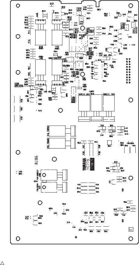
 DSP Circuit Board
to SUB2-CN801
not connected
not installed |
not installed |
Component side
30 |
2NA-WW59820 3 |
 Loading...