


XM-5040X

XM-5040X
SERVICE MANUAL
This set has almost the same specifications as the XM-504X.
This service manual only describes the differences from the XM-504X.
Refer to the appropriate service manual for XM-504X (9-925-592-S) for other
information.
AEP Model
UK Model
MICROFILM
STEREO POWER AMPLIFIER
1
THIS NOTE IS COMMON FOR PRINTED WIRING BOARDS
AND SCHEMATIC DIAGRAMS.
For schematic diagrams
• All capacitors are in µF unless otherwise noted. pF: µµF
50 WV or less are not indicated except for electrolytics
and tantalums.
• All resistors are in Ω and 1/
specified.
4
W or less unless otherwise
• % : indicates tolerance.
f
•
: internal component.
• 2 : nonflammable resistor.
• C : panel designation.
• U : B+ Line.
• V : B– Line.
• Power voltage is dc 14.4V and fed with regulated dc power
supply from +12V terminal (CN901).
• Voltages are tak en with a V OM (Input impedance 10 MΩ).
Voltage variations may be noted due to normal production tolerances.
• Signal path.
F : AUDIO
For printed wiring boards
• X : parts extracted from the component side.
• Y : parts extracted from the conductor side.
• b : Pattern from the side which enables seeing.
• SemiconductorLocation
Ref. No. Location
D101 E-7
D102 E-7
D201 E-8
D202 E-8
D301 D-7
D302 D-7
D401 D-8
D402 D-8
D901 E-13
D902 E-15
D903 F-10
D904 F-11
D905 F-12
D906 A-12
D907 F-12
D908 A-11
D909 E-12
D910 D-9
D911 D-9
D912 E-11
D913 E-11
D914 D-11
D915 C-9
D916 C-9
D930 G-9
IC101 F-3
IC301 D-2
IC901 D-9
IC902 G-11
Q102 F-7
Q103 F-6
Q104 F-6
Q105 F-7
Q106 H-7
Q107 H-7
Q108 G-6
Q109 G-7
Q110 H-5
Q111 H-7
Q112 H-5
Q202 F-8
Q203 F-7
Q204 F-7
Q205 F-8
Q206 H-9
Ref. No. Location
Q207 H-9
Q208 G-7
Q209 G-8
Q210 H-8
Q211 H-9
Q212 H-10
Q302 D-7
Q303 D-6
Q304 C-6
Q305 C-7
Q306 A-7
Q307 A-6
Q308 C-6
Q309 C-7
Q310 B-6
Q311 A-7
Q312 B-7
Q402 D-8
Q403 D-7
Q404 C-7
Q405 C-8
Q406 A-9
Q407 A-9
Q408 C-7
Q409 C-8
Q410 A-8
Q411 A-9
Q412 B-8
Q901 G-15
Q902 E-14
Q903 E-14
Q904 F-9
Q905 F-9
Q906 H-10
Q907 G-10
Q908 H-12
Q909 H-13
Q910 H-11
Q911 H-11
Q912 D-9
Q914 D-11
Q915 D-11
Q916 F-9
Q917 F-9
Q918 F-8
Q919 C-10
Q920 C-9
2
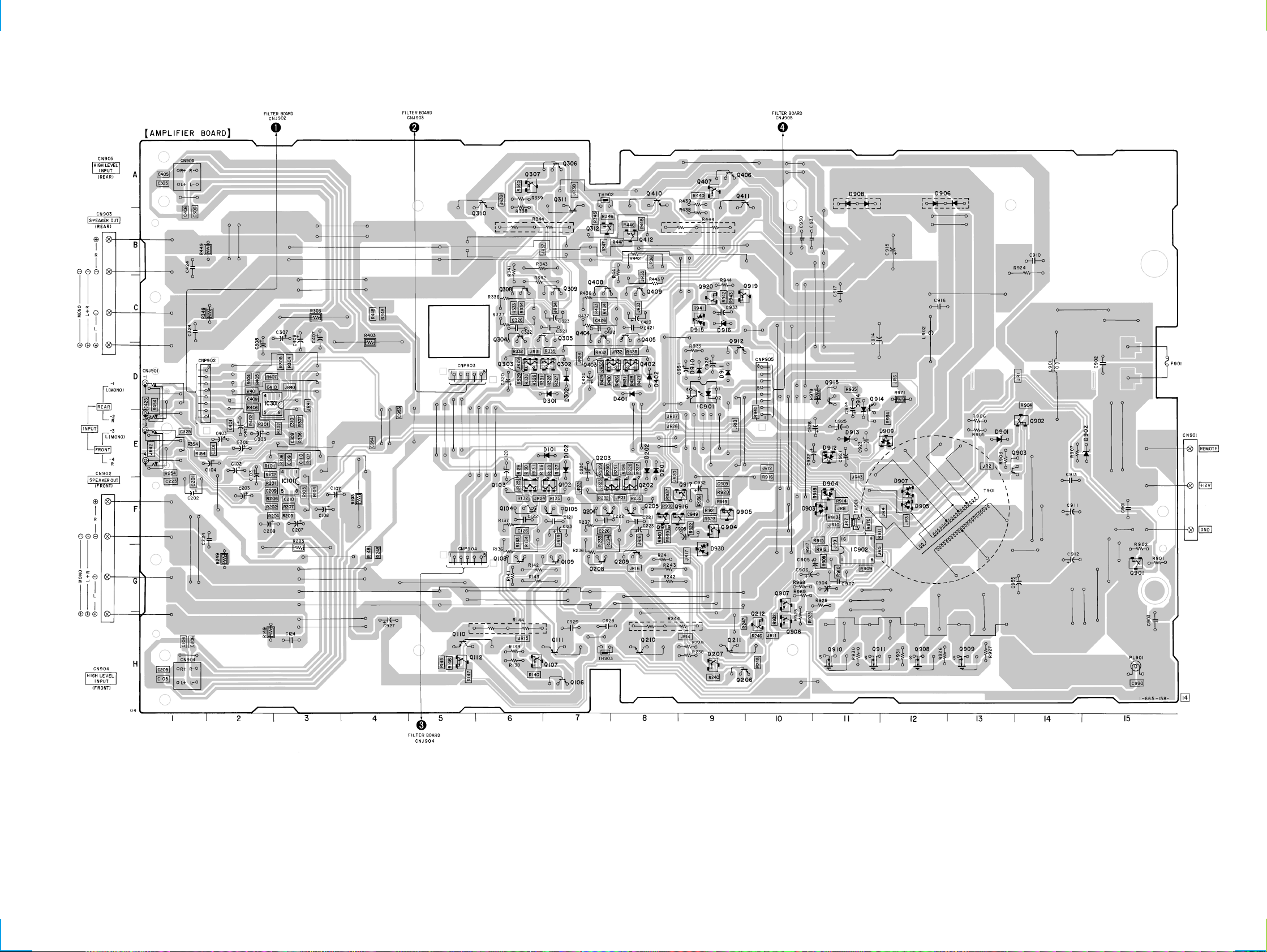
1. PRINTED WIRING BOARD — AMPLIFIER SECTION —
XM-5040X
(Page 6)(Page 6)(Page 6)
(Page 6)
33
XM-5040X
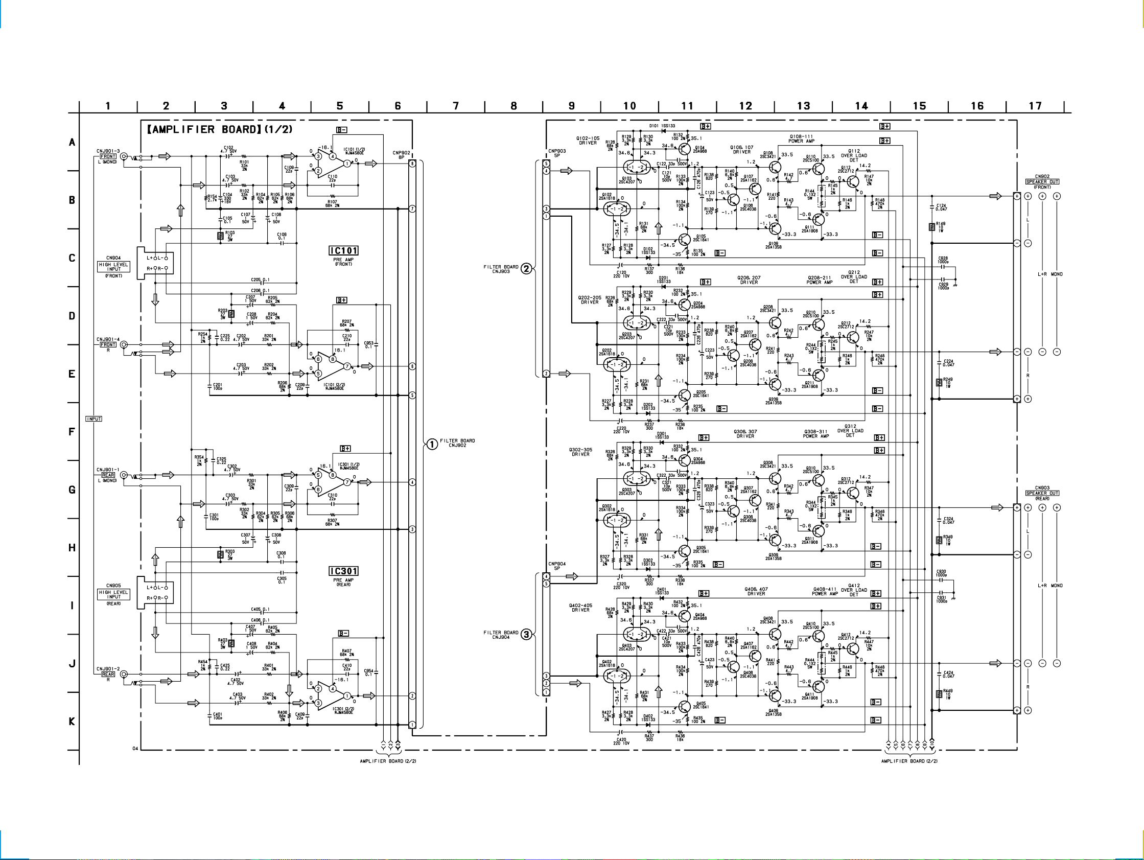
2. SCHEMATIC DIAGRAM — AMPLIFIER SECTION (1/2) —
(Page 7)
(Page 7)
(Page 7)
(Page 5)
(Page 5)
44
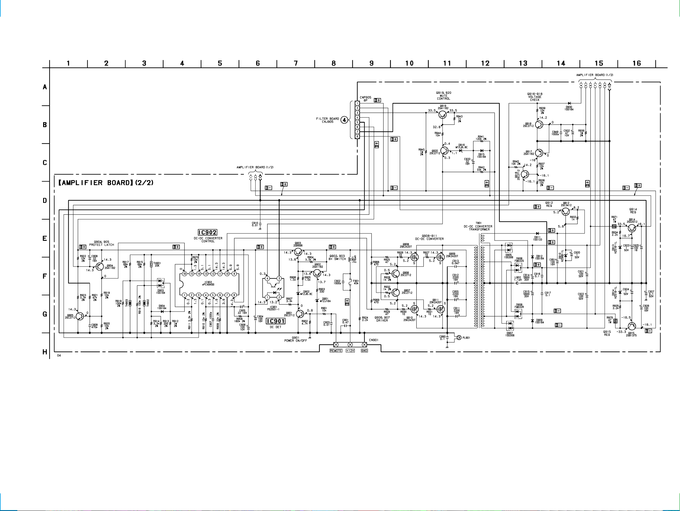
3. SCHEMATIC DIAGRAM — AMPLIFIER SECTION (2/2) —
XM-5040X
(Page 4)
(Page 7)
(Page 4)
55
 Loading...