


TXD-RE210
SERVICE MANUAL
AEP Model
Dolby noise reduction manufactured under license from |
|
Model Name Using Similar Machanism |
NEW |
|
Dolby Laboratories Licensing Corporation. |
|
|||
|
|
|
||
CD |
CD Machanism Type |
CDM28-5BD23 |
||
“DOLBY” and the double-D symbol aare trademarks of |
||||
Dolby Laboratories Licensing Corporation. |
Section |
Base Unit Name |
BU-5BD23 |
|
|
|
|
|
|
|
|
Optical Pick-up Type |
KSS-213B/S-N |
|
|
|
|
|
|
|
Tape deck |
Model Name Using Similar Machanism |
TXD-R11 |
|
|
|
|
|
|
|
Section |
Tape Transport Mechanism Type |
TCM-190RB52C |
|
|
|
|
|
SPECIFICATIONS
COMPACT DISC CASSETTE DECK
MICROFILM

|
TABLE OF CONTENTS |
|
Specifications ........................................................................... |
1 |
|
1. |
SERVICING NOTE .......................................................... |
3 |
2. |
GENERAL |
|
|
Location and Function of Controls .................................... |
4 |
3.DISASSEMBLY
3-1. |
Front Panel Removal .................................................. |
5 |
3-2. CD Mechanism Removal ........................................... |
5 |
|
3-3. |
Mechanism Deck Removal ......................................... |
6 |
4.ADJUSTMENTS
4-1. |
Mechanical Adjustments ............................................ |
7 |
4-2. |
Electrical Adjustments ................................................ |
7 |
5. EXPLANATION OF IC TERMINALS .......................... |
11 |
|
6.DIAGRAMS
6-1. |
Printed Wiring Boards – BD Section – ..................... |
14 |
6-2. Schematic Diagram – BD Section – ......................... |
17 |
|
6-3. |
Schematic Diagram – Main Section – ...................... |
22 |
6-4. |
Printed Wiring Boards – Main Section – .................. |
27 |
7.EXPLODED VIEWS
7-1. Chassis Section ......................................................... |
30 |
|
7-2. Panel Section ............................................................ |
31 |
|
7-3. |
Mechanism Section -1 .............................................. |
32 |
7-4. |
Mechanism Section -2 .............................................. |
33 |
7-5. |
CD Mechanism Section -1 ........................................ |
34 |
7-6. |
CD Mechanism Section -2 ........................................ |
35 |
8. ELECTRICAL PARTS LIST ........................................ |
36 |
|
Laser component in this product is capable of emitting radiation exceeding the limit for Class 1.
This appliance is classified as a CLASS 1 LASER product.
The CLASS 1 LASER PRODUCT MARKING is located on the rear exterior.
This caution label is located inside the unit.
CAUTION
Use of controls or adjustments or performance of procedures other than those specified herein may result in hazardous radiation exposure.
SAFETY-RELATED COMPONENT WARNING!!
COMPONENTS IDENTIFIED BY MARK !OR DOTTED LINE WITH MARK !ON THE SCHEMATIC DIAGRAMS AND IN THE
PARTS LIST ARE CRITICAL TO SAFE OPERATION. REPLACE THESE COMPONENTS WITH SONY PARTS WHOSE
PART NUMBERS APPEAR AS SHOWN IN THIS MANUAL OR IN SUPPLEMENTS PUBLISHED BY SONY.
– 2 –

SECTION 1
SERVICING NOTE
NOTES ON HANDLING THE OPTICAL PICK-UP BLOCK OR BASE UNIT
The laser diode in the optical pick-up block may suffer electrostatic breakdown because of the potential difference generated by the charged electrostatic load, etc. on clothing and the human body.
During repair, pay attention to electrostatic breakdown and also use the procedure in the printed matter which is included in the repair parts.
The flexible board is easily damaged and should be handled with care.
NOTES ON LASER DIODE EMISSION CHECK
The laser beam on this model is concentrated so as to be focused on the disc reflective surface by the objective lens in the optical pickup block. Therefore, when checking the laser diode emission, observe more than 30 cm away from the objective lens.
CHUCK PLATE JIG ON REPAIRING
On repairing CD section, playing a disc without the CD lid, use Chuck Plate Jig.
r Code number of Chuck Plate Jig : X-4918-255-1
r Disc table getting out procedure on the power supply is OFF.
Disc table
3
1
2
– 3 –
SECTION 2 GENERAL
This section is extracted from instruction manual.
LOCATION AND FUNCTION OF CONTROLS
1 |
2 3 4 56 7 8 |
9 |
!º !¡ |
||||||||||||||||
|
|
|
|
|
|
|
|
|
|
|
|
|
|
|
|
|
|
|
|
|
|
|
|
|
|
|
|
|
|
|
|
|
|
|
|
|
|
|
|
|
|
|
|
|
|
|
|
|
|
|
|
|
|
|
|
|
|
|
|
|
|
|
|
|
|
|
|
|
|
|
|
|
|
|
|
|
|
|
|
|
|
|
|
|
|
|
|
|
|
|
|
|
|
|
|
|
|
|
|
|
|
|
|
|
|
|
|
|
|
|
|
|
|
|
|
|
|
|
|
|
|
|
|
|
|
|
|
|
|
|
|
|
|
|
|
|
|
|
|
|
|
|
|
|
|
|
|
|
|
|
|
|
|
|
|
|
|
|
|
|
|
@£ |
|
|
@¡ @º !ª !• !¶!§ |
! |
|
|
|
|
|
|
|
|
|
|
|
|
|||||
|
|
|
|
|
|
|
|
|
|
|
|
|
|||||||||
@™ |
|
!¢ |
|
|
|
!£ |
!™ |
||||||||||||||
|
|
|
1 |
POWER switch |
|
|
|
|
|
|
|
! CD operating buttons |
|
|
|||||||
|
|
|
2 |
Disc tray |
|
|
|
|
|
|
|
|
|
) ± button |
|
|
|||||
|
|
|
3 |
PLAY MODE button |
|
|
|
|
|
|
|
|
|
0 button |
|
|
|||||
|
|
|
4 |
OPEN/CLOSE button |
|
|
|
|
|
|
|
|
|
· button |
|
|
|||||
|
|
|
5 |
REPEAT button |
|
|
|
|
|
|
|
|
|
p |
(stop) button |
|
|
||||
|
|
|
6 |
CD SYNCHRO button |
|
|
|
|
|
|
|
|
|
P |
(pause) button |
|
|
||||
|
|
|
7 |
FADER button |
|
|
|
|
|
|
|
!§ RESET button |
|
|
|||||||
|
|
|
8 |
ARL button |
|
|
|
|
|
|
|
!¶ DISPLAY button |
|
|
|||||||
|
|
|
9 |
Cassette deck |
|
|
|
|
|
|
|
!• TIME button |
|
|
|||||||
|
|
|
!º REC LEVEL control/AUTO indicator |
|
|
!ª |
EDIT/TIME FADE button |
|
|
||||||||||||
|
|
|
!¡ |
DOLBY NR switch |
|
|
|
|
|
|
|
@º |
CREAR button |
|
|
||||||
|
|
|
!™ |
DIRection MODE switch |
|
|
|
|
|
|
|
@¡ |
CHECK button |
|
|
||||||
|
|
|
!£ |
Eject button |
|
|
|
|
|
|
|
@™ |
PHONES jack |
|
|
||||||
|
|
|
!¢ |
Tape operating buttons |
|
|
|
|
|
|
|
@£ |
PHONE LEVEL control |
|
|
||||||
|
|
|
|
r |
REC button |
|
|
|
|
|
|
|
|
|
|
|
|
|
|
|
|
|
|
|
|
R |
REC MUTE button |
|
|
|
|
|
|
|
|
|
|
|
|
|
|
|
|
|
|
|
|
0, ) buttons |
|
|
|
|
|
|
|
|
|
|
|
|
|
|
|
||
|
|
|
|
ª, · buttons |
|
|
|
|
|
|
|
|
|
|
|
|
|
|
|
||
|
|
|
|
p |
(stop) button |
|
|
|
|
|
|
|
|
|
|
|
|
|
|
|
|
|
|
|
|
P |
(pause) button |
|
|
|
|
|
|
|
|
|
|
|
|
|
|
|
|
– 4 –

SECTION 3
DISASSEMBLY
Note : Follow the disassembly procedure in the numerical order given.
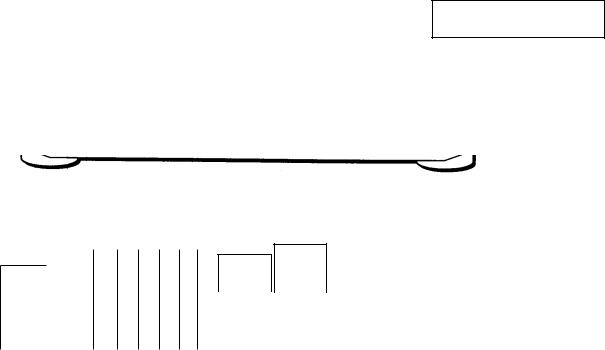
3-1. FRONT PANEL REMOVAL
Disc table
3
1
2
Loading panel
Chassis
4 |
5 Screw (+BV TP 3 x 6) |
6Wire (Flat type) (7 core) to Main board (CN806)
7Wire (Flat type) (23 core) to Main board (CN805)
8Wire (Flat type) (7 core) to Main board (CN801)
9Wire (Flat type) (9 core) to Main board (CN804)
5 Three Screws (+BV TP 3 x 6) |
Front panel assy |
|
3-2. CD MECHANISM REMOVAL
1 Four Screws (+BV TP 3 x 6)
CD Mechanism
2 SN802 (6P)
3
Chassis
– 5 –

3-3. MECHANISM DECK REMOVAL
3 Two Screws (+BV TP 2.6 x 8)
Casstte lid assy |
Front panel assy |
|
Mechanism deck
4
2
1 Press §button
3 Two Screws (+BV TP 2.6 x 8)
– 6 –

SECTION 4
ADJUSTMENTS
4-1. MECHANICAL ADJUSTMENTS
PRECAUTION
1.Clean the following parts with a denatured-alcohol-moistened swab :
record/playback head |
pinch roller |
erase head |
rubber belts |
capstan |
|
2.Demagnetize the record/playback head with a head demagnetizer.
3.Do not use a magnetized screwdriver for the adjustments.
4.After the adjustments, apply suitable locking compound to the parts adjusted.
5.The adjustments should be performed with the rated power supply voltage unless otherwise noted.
rTorque Measurement
Mode |
Torque Meter |
Meter Reading |
||
|
|
|
||
Forward |
CQ-102C |
30 to 65 g•cm |
||
(0.42 – 0.9 oz•inch) |
||||
|
|
|||
|
|
|
|
|
Forward |
CQ-102C |
1 to |
7 g•cm |
|
Back Tension |
|
(0.0134– |
0.097 oz•inch) |
|
|
|
|
|
|
Reverse |
CQ-102RC |
30 to |
65 g•cm |
|
(0.41 – 0.9 oz•inch) |
||||
|
|
|||
|
|
|
|
|
Reverse |
CQ-102RC |
1 to |
7 g•cm |
|
Back Tension |
|
(0.0134– |
0.097 oz•inch) |
|
|
|
|
||
FF, REW |
CQ-201B |
70 to 120 g•cm |
||
(0.972– |
1.66 oz•inch) |
|||
|
|
|||
|
|
|
|
|
4-2. ELECTRICAL ADJUSTMENTS
1.The adjustment should be performed in the publication. (Be sure to make playback adjustment at first.)
2.The adjustment and measurement should be performed for
both L-CH and R-CH. |
|
r Switch position |
|
DOLBY NR switch |
: OFF |
DIR MODE switch |
:A |
r Standard record position : |
|
Deliver the standard input signal level to input jack and set the REC LEVEL control to obtain the standard output signal level as follows.
Record Mode
AF OSC
TAPE IN |
level meter |
|
10 kΩ |
47 kΩ |
attenuator |
|
|
+ |
|
set |
|
– |
600 Ω |
|
|
TAPE OUT |
r Standard Input Level
Input Terminal |
TAPE IN |
|
|
source impedance |
10kΩ |
|
|
input signal level |
0.5V (–3.8dB) |
r Standard Output Level |
|
|
|
Output Terminal |
TAPE OUT |
|
|
load impedance |
47kΩ |
|
|
output signal level |
0.5V (–3.8dB) |
|
|
rTest tape
Tape |
Contents |
Use |
|
|
|
|
|
P-4-A100 |
10 kHz, |
–10dB |
Azimuth Adjustment |
|
|
|
|
P-4-L300 |
315Hz, |
0dB |
PB Level Adjustment |
|
|
|
|
WS-48B |
3kHz, |
0dB |
Tape Speed Adjustment |
0dB=0.775V
TC Test Mode
setting : Push POWER button with STOP key and REC MUTE key.
function : r when start recording, COUNTER is set to “0000” and COUNTER MEMORY function is effective (“MEMORY” appears on FLD).
r While playing or AMS, the signal level is displayed. (“L” / “H”)
rTest tape
Tape |
Contents |
Use |
|
|
|
|
|
P-4-A100 |
10 kHz, |
–10dB |
Head Azimuth Adjustment |
|
|
|
|
P-4-L300 |
315Hz, |
0dB |
Level Adjustment |
|
|
|
|
WS-48B |
3kHz, |
0dB |
Tape Speed Adjustment |
|
|
|
|
0dB=0.775V
Record/Playback Head Azimuth Adjustment
r Carrey out servicing or repairs form the REVERSE direction
first.
Procedure :
1. Mode : Forward playback
test tape |
|
|
P-4A100 |
level meter |
|
(10kHz, –10dB) |
||
47 kΩ |
||
|
||
|
+ |
|
|
set |
|
|
– |
TAPE OUT
2.Turn the adjustment screw for the maximum output levels. If these levels do not match, turn the adjustment screw until both of output levels match together within 1dB.
|
L-CH |
|
|
|
peak |
|
|
|
output |
within |
within |
|
1 dB |
||
|
level |
1 dB |
|
|
|
||
|
R-CH |
|
|
Screw |
peak |
|
|
|
|
|
|
position |
|
|
|
|
|
|
screw angle |
|
|
L-CH |
R-CH |
|
|
peak |
peak |
– 7 –

3. Playback Mode
test tape P-4A100
(10kHz, –10dB)
Osilloscope
L-CH |
47 kΩ |
V H
set
R-CH |
47 kΩ |
|
|
TAPE OUT |
|
screen pattern |
|
|
in phase 45° |
90° 135° |
180° |
good |
wrong |
|
4.Change the reverse playback mode and repeat the steps 1 to 3.
5.After the adjustment, lock the adjustment screw with suitable locking compound.
Adjustment Location :
– record/playback head –
forward side |
revers side |
adjustment screws
Tape Speed Adjustment
Procedure :
Mode : Playback
test tape |
|
WS-48B |
|
(3kHz, 0dB) |
frequency counter |
|
47 kΩ |
set |
+ |
|
– |
TAPE OUT
1.Set to forward playback mode.
2.Adjust RV71 so that frequency reading becomes 3,000± 90Hz.
Frequency difference between the beginning and the end of the tape should be within ± 3%.
Adjustment Location : AUDIO board. (see page 9)
Sample Value of Wow and flutter
W. RMS (JIS) within 0.3% (test tape : WS-48B)
Playback Level Adjustment
Procedure :
Mode : Playback
test tape |
|
|
P-4-L300 |
level meter |
|
(315Hz, 0dB) |
||
47 kΩ |
||
|
||
|
+ |
|
|
set |
|
|
– |
TAPE OUT
Adjust RV11 (L-CH) and RV21 (R-CH) so the level meter reading becomes the adjustment limits below.
Adjustment Level :
TAPE OUT level : – 7.7± 0.5dB (0.301 to 0.338V) Level Difference between Channels : within 0.5dB
Confirm the TAPE OUT level does not change in playback mode while changing the mode from playback to stop several times.
Adjustment Location : AUDIO board. (see page 9)
Record Bias Adjustment
Procedure :
1. Mode : Record
AF OSC 1) 315Hz |
72.3mV (–20.6dB) |
blank tape |
|
2) 10kHz |
|||
|
|||
|
|
CS-123 |
|
attenuator |
10 kΩ |
|
|
|
|
||
|
set |
|
600Ω
TAPE IN
2. Mode : Playback
recorded |
level meter |
|
portion |
||
47 kΩ |
||
|
||
|
+ |
|
|
set |
|
|
– |
TAPE OUT
3.Confirm playback the signal recorded in step 1 become adjustment level as follows.
4.If these levels do not adjustment level, adjust the RV12 (L-CH) and RV22 (R-CH) to repeat step 1 and 4.
Adjustment level : Playback output of 315Hz to playback output of 10kHz : ±0.5dB.
Adjustment Location : AUDIO board.
– 8 –
Record Level Adjustment
Procedure :
1. Mode : Record
AF OSC
315Hz 72.3mV (–20.6dB) |
blank tape |
|
|
|
CS-123 |
10 kΩ
attenuator
set
600Ω
TAPE IN
2.Mode : Playback
recorded |
level meter |
|
portion |
||
47 kΩ |
||
|
||
|
+ |
|
|
set |
|
|
– |
TAPE OUT
3.Confirm playback the signal recorded in step 1 become adjustment level as follows.
4.If these levels do not adjustment level, adjust the RV111 (L-CH) and RV211 (R-CH) to repeat step 1 and 4.
Adjustment Level :
TAPE OUT level : – 26± 0.5dB (36.7 to 41.1mV)
Adjustment Location : MAIN board.
[AUDIO BOARD] (Conductor side)
Record Bias
(R) (L) RV22 RV12
RV71 (NORMAL) Tape speed
RV21(R)
Playback Level
RV11(L)
[MAIN BOARD]
(Component side) |
RV211 : Record level (R-CH) |
RV111 : Record level (L-CH)
CD SECTION
Note :
1.CD Block basically constructed to operate without adjustment. Therefore, check each item in order given.
2.Use YEDS-18 disc (3-702-101-01) unless otherwise indicated.
3.Use the oscilloscope with more than 10MΩ impedance.
4.Clean an object lens by an applicator with neutral detergent when the signal level is low than specified value with the following checks.
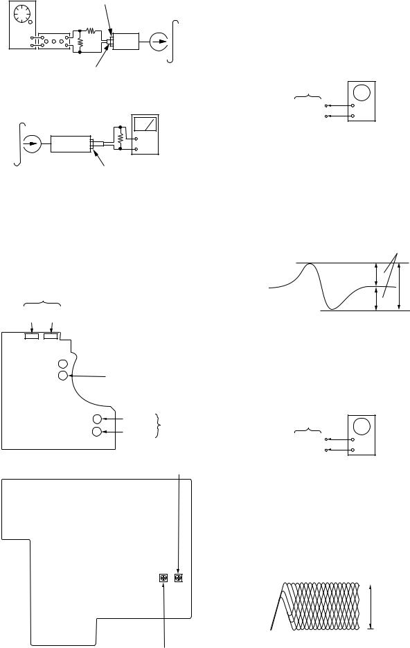
S-Curve Check
|
oscilloscope |
BD board |
|
TP (FE) |
+ |
TP (VC) |
– |
Procedure :
1.Connect oscilloscope to test point TP(FE) and BD board.
2.Connect between test point TP (FEI) and TP (VC) by lead wire.
3.Turned Power switch on.
4.Put disc (YEDS-18) in and turned Power switch on again and actuate the focus search. (Actuate the focus search when disc table is moving in and out.)
5.Check the oscilloscope waveform (S-curve) is symmetrical between A and B. And confirm peak to peak level within
3 ±1Vp-p.
symmetry
A
within 3 ±1Vp-p
B
6. After check, remove the lead wire connected in step 2.
r Try to measure several times to make sure that the ratio of A : B or B : A is more than 10 : 7.
rTake sweep time as long as possible and light up the brightness to obtain best waveform.
RF Level Check
|
oscilloscope |
BD board |
|
TP (RF) |
+ |
TP (VC) |
– |
Procedure :
1.Connect oscilloscope to test point TP (RF) on BD board.
2.Turned Power switch on.
3.Put disc (YEDS-18) in and playback.
4.Confirm that oscilloscope waveform is clear and check RF signal level is correct or not.
Note :
Clear RF signal waveform means that the shape “ à ” can be clearly distinguished at the center of the waveform.
RF signal waveform |
|
VOLT/DIV : 200mV |
|
|
TIME/DIV : 500nS |
|
|
|
level : 1.2 +0.25–0.20Vp-p
– 9 –

E-F Balance (1 Track Jump) Check
|
oscilloscope |
|
(DC range) |
BD board |
|
TP (TE) |
+ |
TP (VC) |
– |
Procedure :
1. Connect oscilloscope to test point TP(TE) on BD board. 2. Turned Power switch on.
3. Put disc (YEDS-18) in to play the number five track.
4. Press the “ P(Pause)” button. (Becomes the 1 track jump mode) 5. Check the level B of the oscilloscope’s waveform and the A (DC
voltage) of the center of the Traverse waveform. Confirm the following :
A/B x 100 = less than ±22%
1 track jump waveform
Center of the waveform
B
A (DC voltage)
0V
level : 1.3 ±0.6 Vp-p |
symmetry |
RF PLL Free-run Frequency Check
Procedure :
1. Connect frequency counter to test point (PLCK) with lead wire.
frequency counter
BD board
TP (PLCK) 
 +
+
 –
–
2.Turned Power switch on.
3.Put disc (YEDS-18) in to play the number five track. Confirm that reading on frequency counter is 4.3218MHz.
Adjustment Location :
[BD BOARD] (Side B)
|
10 |
|
5 |
1 |
|
11 |
|
15 |
|
20 |
|
TE |
|
FE |
|
|
|
VC |
|
|
|
RF |
|
PLCK |
|
|
TEI |
|
|
|
|
|
|
|
|
|
14 |
10 |
|
5 |
1 |
15 |
20 |
|
25 28 |
||
– 10 –
|
|
|
|
|
SECTION 5 |
|
|
|
EXPLANATION OF IC TERMINALS |
||
IC801 µPD78044FGF029-3B9 (SYSTEM CONTROL) |
|||||
|
|
|
|
|
|
Pin No. |
Pin name |
|
I/O |
|
Description |
|
|
|
|
|
|
1 |
LED |
|
O |
|
AUTO REC LEVEL LED ON/OFF. |
|
|
|
|
|
|
2–7 |
1G – 6G |
|
O |
|
FL grid drive. |
|
|
|
|
|
|
8 |
VDD |
|
– |
|
Power supply (+5V) |
|
|
|
|
|
|
9 |
CLK |
|
O |
|
Command clock output for IC101 and IC104. |
|
|
|
|
|
|
10 |
DATA |
|
O |
|
Command data output for IC101 and IC104. |
|
|
|
|
|
|
11 |
SENS |
|
I |
|
SENS input for IC101 and IC104. |
|
|
|
|
|
|
12 |
PGML |
|
O |
|
Command latch output for IC104. |
|
|
|
|
|
|
13 |
AMUTE |
|
O |
|
Mute control output. |
|
|
|
|
|
|
14 |
SQCLK |
|
O |
|
Q-data read-out for clock output. |
|
|
|
|
|
|
15 |
NC |
|
O |
|
Not used (Open). |
|
|
|
|
|
|
16 |
SUBQ |
|
I |
|
Q-data input. |
|
|
|
|
|
|
17 |
––––––––––––––– |
|
I |
|
System reset input. |
RESET |
|
|
|||
18 |
METAL |
|
I |
|
Metal tape detect input. |
|
|
|
|
|
|
19 |
––––––––––––––––––– |
|
I |
|
TC test mode input. “L” : Test mode. |
TC TEST |
|
|
|||
|
|
|
|
|
|
20 |
AVSS |
|
– |
|
A/D ground terminal. |
|
|
|
|
|
|
21 |
LD IN |
|
O |
|
CD loading-in output. |
|
|
|
|
|
|
22 |
LD OUT |
|
O |
|
CD loading-out output. |
|
|
|
|
|
|
23 |
AD CTRL1 |
|
O |
|
A/D extended input (1) select signal output. |
|
|
|
|
|
|
24 |
AD CTRL0 |
|
O |
|
A/D extended input (0) select signal output. |
|
|
|
|
|
|
25 |
AD1 |
|
I |
|
A/D extended input (1). |
|
|
|
|
|
|
26 |
AD0 |
|
I |
|
A/D extended input (0). |
|
|
|
|
|
|
27 |
S. REEL |
|
I |
|
Supply reel pulse input. |
|
|
|
|
|
|
28 |
CD TEST |
|
I |
|
CD test mode input. |
|
|
|
|
|
|
29 |
AVDD |
|
– |
A/D analog power supply. |
|
|
|
|
|
|
|
30 |
AVREF |
|
I |
|
A/D reference voltage input. |
|
|
|
|
|
|
31 |
STOP SW |
|
I |
|
STOP switch input. |
|
|
|
|
|
|
32 |
XT2 |
|
– |
|
Not used (Open). |
|
|
|
|
|
|
33 |
VSS |
|
– |
|
Ground terminal. |
|
|
|
|
|
|
34 |
X1 |
|
I |
|
System clock. (4MHz) |
|
|
|
|
|
|
35 |
X2 |
|
O |
|
System clock. (4MHz) |
|
|
|
|
|
|
36 |
NR1 |
|
O |
|
Dolby mode select output (1). |
|
|
|
|
|
|
37 |
NR0 |
|
O |
|
Dolby mode select output (2). |
|
|
|
|
|
|
38 |
––––––––––– |
|
O |
|
Blank skip/AMS select output. |
BS/AMS |
|
|
|||
|
|
|
|
|
|
39 |
––––––––––––––– |
|
O |
|
REC/PLAY select output. |
RELAY |
|
|
|||
|
|
|
|
|
|
40 |
XLT |
|
O |
|
Command lucth output. |
|
|
|
|
|
|
41 |
REEL– |
|
O |
Reel motor control output. |
|
|
|
|
|
|
|
42 |
REEL+ |
|
O |
|
Reel motor control output. |
|
|
|
|
|
|
43 |
VOL OUT |
|
O |
|
Electrical volume control. |
|
|
|
|
|
|
44 |
–––––––––––––––––––––––– |
|
O |
|
REC mute ON/OFF control. |
REC MUTE |
|
|
|||
|
|
|
|
|
|
45 |
POWER OUT |
|
O |
|
Power switch control. |
|
|
|
|
|
|
46 |
SCOR |
|
I |
|
Q-data sync input. |
|
|
|
|
|
|
47 |
SIRCS IN |
|
I |
|
Remote control signal input. |
|
|
|
|
|
|
48 |
VSS (IC) |
|
– |
|
Ground terminal. |
|
|
|
|
|
|
49 |
AMS IN |
|
I |
|
AMS signal input. |
|
|
|
|
|
|
50 |
POWER IN |
|
I |
|
Power OFF detect input. |
|
|
|
|
|
|
– 11 –

Pin No. |
Pin name |
I/O |
Description |
|
|
|
|
51 |
LD ON |
O |
Laser diode ON output. |
|
|
|
|
52 |
VDD |
– |
Power supply (+5V). |
|
|
|
|
53 |
HP SEL |
O |
Headphone output selection. |
|
|
|
|
54 |
INPUT SEL |
O |
Recording source select. |
|
|
|
|
55 |
–––––––––––––––––––––––––––––––– |
|
|
TC LINE MUTE |
O |
TC line mute control output. |
|
|
|
|
|
56–70 |
S1–S15 |
O |
FL segment output. |
|
|
|
|
71 |
VDISP |
– |
Power supply for FL. |
|
|
|
|
72–77 |
S16–S21 |
O |
FL segment output. |
|
|
|
|
78 |
BIAS |
O |
Bias ON/OFF output. |
|
|
|
|
79 |
PB/REC |
O |
PB/REC select output for Dolby (IC501). |
|
|
|
|
80 |
CAP.M |
O |
Capstan motor ON/OFF control. |
|
|
|
|
– 12 –

SECTION 6
DIAGRAMS
r CIRCUIT BOARDS LOCATION
BD board TRANSFORMER board
POWER SW board
LEAF SW board
HP board
LOADING board
PANEL board
MAIN board
AUDIO board
VOL board
– 13 –
– 14 –
 Loading...