


D99 CHASSIS
OPERATION MANUAL
TROUBLESHOOTING MANUAL
TABLE OF CONTENTS |
|
CIRCUIT DESCRIPTION |
|
D Board (Power Supply Section) ............. |
2 |
D Board (Deflection Section) ................... |
9 |
A Board .................................................. |
20 |
GENERAL TROUBLESHOOTING .............. |
26 |
PARTS LEVEL BOARD REPAIR ................ |
37 |
TRINITRON® COLOR COMPUTER DISPLAY
- 1 -
CIRCUIT DESCRIPTION
D BOARD POWER SUPPLY SECTION
Power Supply Electrical Circuit
The power supply is located on the D Board. It has three modes of operation that are controlled by a microprocessor. The topology is a discontinuous mode flyback converter with photocoupler feedback for regulating the secondary voltages. Circuit operation and troubleshooting are explained in the following sections:
Operation Modes |
Secondary Circuitry |
AC Input |
Protection Circuits |
Degauss Circuit |
Troubleshooting |
Primary Circuitry |
|
Operation Modes |
|
The power supply has four modes of operation, ‘off’, ‘active off’, ‘suspend/standby’ and ‘active on’. These modes are related to power savings and are indicated by the front panel LED. Additional indications are failure diagnostics and aging mode. The table below lists operation mode, condition and LED status.
Mode |
Syncs |
Condition |
LED |
Off |
N/A |
Power Switch Off |
Off |
Active Off |
No H and V |
Low Power, Heater Off |
Amber |
Suspend/Standby |
No H or V |
Low Power, Heater On |
Amber 0.5s<- ->Green 0.5s |
Active On |
H and V Present |
Phase Locked, Normal Operation |
Green |
Failure 1 |
NA |
HV or +B Failure |
Amber 0.5s<- ->Off 0.5s |
Failure 2 |
NA |
H Stop, V Stop, Thermal Failure |
Amber 1.5s<- ->Off 0.5s |
Failure 3 |
NA |
ABL Failure |
Amber 0.5s<- ->Off 1.5s |
Aging/Self Test |
No H and V |
Aging Raster or Test Pattern |
Green 0.5s<- ->Off 0.5s |
Except for power switch off, all modes of operation are controlled by the microprocessor located on the D Board. The failure modes are detected by the microprocessor and the power supply is forced into active off mode. These functions are discussed later (Deflection).
With the AC cord attached to the monitor and connected to an AC source, the monitor will be off until the power switch is turned on. When the power switch is turned on, the power supply starts and is in active off mode. The next step is active on mode. The power saving modes are activated by the microprocessor based upon the presence of either H or V sync. If no sync signals are present, the power supply is set to active off mode. If only horizontal sync is present the power supply moves to suspend mode. If only vertical sync is present the power supply enters standby mode.
Power supply operation control signals are “Remote On/Off” and “Heater On/Off”. Remote On/Off is digital low for active off and suspend/standby modes. Heater On/Off is digital low for active off mode. To enter active on mode, the microprocessor must set remote on/off to digital high. Heater on/off is also made digital high and the heater is turned on.
Output |
Off |
Active Off |
Suspend/Standby |
Active On |
B+ |
0V |
13V |
180V |
180V |
80V |
0V |
10V |
77V |
79V |
+15V |
0V |
1V |
14V |
+15V |
-15V |
0V |
-1V |
-14V |
-15V |
+12V |
0V |
0V |
0V |
+12V |
5V |
0V |
0V |
0V |
+5V |
H eater |
0V |
0V |
4.6V |
6.3V |
H . C entering |
0V |
|
+7V |
+10V |
STB Y 5V |
0V |
+5V |
+5V |
+5V |
- 2 -
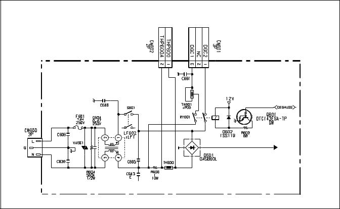
AC Input and Degauss |
1. AC Input Section
The AC input section provides EMI filtering, input protection, surge limiting and CRT degauss operation.
EMI Filter
The EMI filter comprises CN600 (inlet with filter), X-capacitors C604 and C605, Y-capacitors C606, C638, C660 and C643 and the line filter transformer, LF602. Input protection is provided by F601and VA601; surge current limiting by thermistor TH600 and resistor R600. Degauss is explained in the next section.
Degauss Circuit
The degauss circuit is used to demagnetize the CRT. After power on, the microprocessor located on the D Board sets the degauss signal to digital high and Q601 turns on relay RY601. This allows AC current into the degaussing coil through posistor TH601. The current heats up the posistor and its affective resistance increases, this dampens the current in the degauss coil to nearly zero. Duration time is approximately 5-6 seconds and the microprocessor then shuts off RY601, which disconnects the degauss coil from the AC line. This operation should sufficiently demagnetize the CRT.
2. Primary Circuitry Section
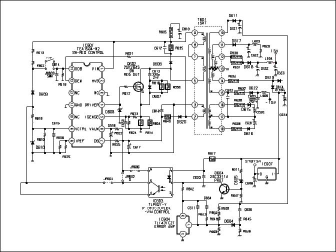
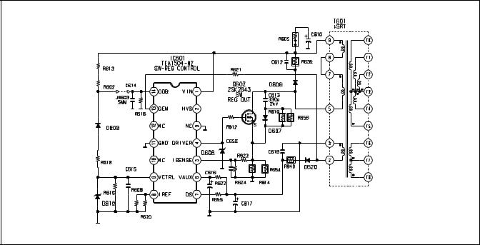
IC601
The heart of the primary section is the TEA1504/N2 power supply controller, IC601. The following describes the functions of each pin.
Pin 1 – Vin: This is a MOSFET drain connection internal to IC601, which is connected directly to the DC mains voltage rail. The startup current source derives power from the DC mains via the Vin pin. It supplies current to charge the Vaux (IC supply) capacitors C616 and C617 and also provides current to the IC601 control circuitry.
Pin 2 – HVS: High voltage safety spacer pin is a no connection.
Pin 3 – NC: Connected to primary side DC mains return.
- 3 -
Pin 4 – Driver: Outputs the pulse width modulated gate drive for switching transistor Q602. Maximum duty cycle is set internally at 80%.
Pin 5 – Isense: Provides cycle by cycle over current protection by turning off pin 4 driver output when Q602 current exceeds the current limit corresponding to 500mV at pin 5. This pin typically provides 425nS of leading edge blanking time. The threshold voltage for switch over to low frequency (low power) operation is sensed by pin 5. When the voltage sensed at pin 5 is below 165mV, IC601 transitions from operating at high frequency (56.5KHz) to low frequency (23.5KHz).
Pin 6 – Vaux: IC601 supply pin. An internal current source from IC601 charges the Vaux capacitors C616 and C617 for startup. Once the Vaux capacitors are charged to the startup voltage level (11V), then IC601 starts switching pin 4 driver output. The Vaux is also supplied by an auxiliary winding from T601 on the primary side once the secondary output voltages attain their nominal operating voltage values. Pin 6 also provides under voltage lockout detection (8V) and over voltage protection (14.7V).
Pin 7 – DS: Provides the power supply for the driver output (pin 4).
Pin 8 – Iref: Controls IC601 internal bias currents, which determines the pulse width modulated switching frequencies. High frequency is 56.5KHz during active on mode. Low frequency is 23.5KHz during suspend/standby mode.
Pin 9 – Vctrl: Feedback voltage for duty cycle control.
Pin 10 – NC: No connection.
Pin 11 – Gnd: Connected to primary side DC mains return.
Pin 12 – NC: No connection.
Pin 13 – Dem: Guarantees discontinuous conduction mode operation for the power supply. Verifies that T601 is demagnetized by not activating the next gate drive pulse until the primary side auxiliary winding of T601 is lower than the threshold level of 65mV as detected at pin 13.
Pin 14 – OOB: On/Off/Burst mode input signal. A voltage greater than 2.5V enables IC601.
Operation
The power supply is a discontinuous-mode flyback converter with photocoupler feedback for regulating the secondary voltages. The PWM controls the pulse width of the gate drive.
When AC is applied to the power supply and IC601 pin 14 is greater than 2.5V, start up current is supplied though IC601 pin 1 to IC601 pin 6. Startup voltage is approximately 11V. After start up, the voltage to pin 6 and pin 7 of IC601 is supplied through D620 connected to T601 pin 2. The first mode of operation is active off mode. The output drive pulse frequency will be in burst mode operation.
When the power supply enters active on mode, the switching frequency will be 56.5KHz. The Vaux level will be approximately 12.5 volts. OVP threshold is 14.7 volts and UVLO is 8.0 volts. Therefore, if the Vaux voltage is not correct, the power supply will not operate properly.
Feedback from the secondary side comes through IC603 and IC604, which is connected to IC601 pin 9. (See diagram on page 5.)
3. Secondary Circuitry Section
The secondary section consists of the following circuits. Rectifier diodes and filters for all output voltages, horizontal centering, +5/12 volt regulators, +5 standby regulator, heater voltage regulator, voltage feedback circuit, active off mode feedback, and protection circuits. This section will describe each circuit and its function.
Secondary Rectifiers
The secondary rectifiers supply the following voltages, 180V (B+) deflection and video, 80V video, ±15V deflection and regulators, 6.3 volt heater regulator, +5V standby regulator, horizontal centering voltages.
- 4 -
Horizontal Centering
This circuit supplies IC503, which is used to adjust horizontal raster position on the CRT. The horizontal centering circuit consists of fusible resistors R638 and R639, diodes D615 and D616 and filter capacitors C630 and C631. In respect to the secondary ground, the horizontal centering ground is floating and connected to –H DY line. The voltages in reference to this floating ground are ±10 volts. Care should be taken to not short the floating ground to the secondary ground.
+5/12 Volt Regulator
IC605 is the 12 volt regulator and IC608 is the 5 volt regulator. The output voltages are supplied to the microprocessor, deflection and video circuits. The +15 volt line provides the input voltage for +12V regulator; the +12V line provides the input voltage for +5V regulator. During active off or suspend/standby mode, the 12 volt regulator is disabled via remote on/ off and subsequently the 5V regulator is disabled.
+5V Standby Circuit
IC607 is the standby 5V regulator. In the active on mode and the suspend/standby mode, the input to the regulator is supplied from T601 winding 14-13. During the active off mode, the regulator input is supplied from T601 winding 10-13 via D612 and D613. Typical input voltages to the regulator are active on mode: 9.5V; suspend/standby mode: 7.4V; active off mode: 11.5V.
Heater Voltage Regulator
Heater filament voltage is supplied by T601 winding 14-13 and is regulated by IC602. IC602 output is turned on and off by the heater on/off control line at pin 1, CTL. The output is off during active off mode.
Feedback Circuit
The feed back circuit is divided into two sections. One is for active on and suspend/standby modes; the other for active off mode. The following two sections explains the theory and operation.
Active On and Suspend/Standby Mode Feedback
Shunt regulator IC604 regulates the B+ line to 179.2V by sinking current through the opto coupler 1C603 to ground. The
- 5 -

Feedback Circuits |
reference voltage at IC604 pin 1 determines the sink current into pin 3. The reference voltage is set to 2.50 volts by resistor divider R608, R650, R648, and R609. Since the B+ is connected to the resistor divider, any change in B+ voltage is detected at the reference terminal. The shunt regulator will either increase or decrease the current into pin 3 in order to decrease or increase the B+ voltage respectively and try to maintain the reference voltage to 2.50 volts. IC603 biases it's phototransistor accordingly and drives IC601 pin 9 (Vctrl) which changes the duty cycle at IC601 pin 4 (driver) to regulate the B+ voltage at 179.2V.
Active Off Mode Feedback
Heater control line is low (heater off) during active off mode and respectively Q603 is off. Voltage pulses from T601 pin 10 flow through C620, R636, and R660 triggering the gate of thyristor D613. D613 turns on effectively shorting the B+ rail to the standby 5V regulator input; current flows from T601 pin 10 through D612 and D613 to the standby 5V regulator input. When the standby 5V regulator input is increased to approximately 12.7V it forward biases zener diode D605 turning on Q604 and sinks current through IC603 to ground. The standby 5V input supplies this current to IC603 pin 1. IC603 biases it's phototransistor and drives current through D609 into IC601 pin 14 (OOB) triggering burst mode operation. IC601 pin 4 (driver) is pulled low turning off switching transistor Q602. T601 pin 2 (auxiliary winding) feedback pulses are discontinued and IC601 pin 6 (Vaux) decreases to 8V. IC601 internal current source then charges pin 6 (Vaux) to the startup voltage level (11V) which starts switching pin 4 driver output. The feedback cycle is then repeated. The burst repetition rate is approximately every 110mS and when IC601 pin 4 is switching its frequency is 23.5KHz.
- 6 -
Protection Circuits
4. Protection Circuits
The following are protection circuits: OCP, OVP, UVLO and secondary short circuits. OCP is pulse by pulse and is performed on the primary side. OVP detects excessive output voltages. UVLO detects output under voltages. The following will explain the operation of these functions.
OCP
OCP is activated if there is too much current passing through the power MOSFET, Q602. This condition will occur if either the B+ line or 80 volt line is shorted.
R614 and R654 are the current sense resistors. Current through these resistors will produce a positive voltage reference to ground. R623, R624 and C650 provide a voltage divider and filter to IC601 pin 5 (Isense). If the voltage level exceeds 0.5 volts, the IC does pulse by pulse current limit and the output voltages are reduced. This condition can be audible and characterized by a ‘chirping’ sound.
OVP and UVLO
The OVP and UVLO functions are detected by IC601 pin 6 (Vaux). Vaux is mornally 12.5V. In the event the regulation control loop were to fail, the output voltages would either increase or decrease; then Vaux would increase or decrease respectively via T601 transformer coupling. IC601 pin 6 will detect an OVP at 14.7V and UVLO at 8V turning off the driver output and initiating a low dissipation safe-restart mode.
Secondary Short Circuits
Safe operation during secondary short circuits is provided by the demag function of IC601 pin 13. Demag protection decreases the switching frequency to a very low level, thereby reducing the input power level and providing safe operation. Demag also provides a soft start function during startup gradually increasing the switching frequency until fixed frequency operation is attained.
5. Troubleshooting
Warning
Before attempting to fix the power supply, safety should be considered first. Never connect test probes to the primary side circuits, unless proper isolation has been installed. If isolation for the AC mains is not present, serious harm can occur. Never assume you are safe.
- 7 -
No Power
In the event that the monitor does not turn on, first verify input power is applied to CN600 and the front panel power switch is turned on; then check F601 and R605. If these parts are blown, the primary side circuitry should be checked. If the fuses are not blown, then check the secondary side circuitry, especially the protection circuits. If these circuits are causing a no power symptom, the problem can be more readily found.
AC Input and Degauss Circuit Trouble Shooting
For no power or nonoperating power supply, the AC input circuitry should be checked. cause non-operation. F601, CN600, and R605 on the D Board should be checked first. for continuity.
Open or short circuit elements will Check the front panel power switch
If all elements are correct, check whether F601 breaks when power is applied and the power switch is closed. If the fuse does blow, there may be problems with the primary circuitry or a component short.
The degauss will malfunction if CN601 is not connected. One problem could be loss of degauss signal from the microprocessor. This can be verified by using the manual degauss command found in the OSD menu. If the signal does not appear at Q601 base, then it is possible that the microprocessor does not function correctly or standby 5V is not functioning.
The second step is to place a short across the AC terminals of RY601 for less than two seconds. If degauss operates then check Q601 and RY601. If degauss does not work, check TH601 for an open condition and VA600 for a short condition.
Primary Section
Three main areas can diagnose primary circuit failures. These are IC601, Q602 and Feedback system. Visible checks of these areas will aid in finding problems. The following will discuss each section.
IC601
First apply AC to the monitor and check IC601 pin 4 output. If the output on pin 4 is not present, there could be problems with Q602 and related parts or pin 14 could be less than 2.5 volts. Further, check Vaux level at pin 6. If it less than 11 volts, the IC could be in safe-restart mode. If the voltage is very low, there could be a short on any of the IC pins. In reference to ground, check the impedance of pin 1, 8 and 14. If any of these pins are shorted, replace the IC and check components connected to the related pins. Take care that C617 and C616 are fully discharged before replacing the IC.
Q602
The switching transistor can be damaged in various ways. These are related to voltage, current and temperature.
Check whether the transistor is shorted across drain and source terminals. If there is a short, F601, R605, R614, R654, R623, R624 and C650 should be checked. Additional components to check are D608, R612 and IC601. If Q602 is shorted, all these parts should be replaced.
Failure of a secondary rectifier diode can also cause Q602 to fail. Check 180V and 80V diodes for open or short conditions. There is also a clamp circuit, which is used to clip the turn off spike found on Q602 drain. If the clamp circuit is broken, it can cause Q602 failures. Check D606, C612 and R635. Also check the snubber circuit components C613, D607, R619 and R656.
Secondary Circuit
Failure in the secondary circuits can be categorized by rectifier diodes, fusible resistors, regulators, feedback loops and protection circuits. These sections are interrelated and failure in one can affect another. Consequently, some failures will also affect the primary circuitry.
Rectifier Section
Rectifier diode failures are not common, but do occur. Deflection, video and high voltage circuitry failures contribute to diode damage. In the event a voltage is not present, check for shorts to ground, open or short diodes. Also check fusible resistors found on the voltage lines.
Horizontal Centering
Loss of horizontal center adjustment can be affected by the rectifier diodes, fusible resistors, IC503 and related circuitry. Measure the voltages in reference to the horizontal centering ground. Typically, the voltages are ±10 volts. However, the adjustment setting can reduce the voltages. If there are no problems found with the diodes or fusible resistors, the next step is to check the adjustment signal at Q506. If the adjustment signal is not present check the IC901 pin 4. Otherwise, check IC503 and related components.
- 8 -
+5/12 Volt Regulator
Loss of voltage due to shorts or device failures on either +12 or +5 volt output lines can occur. Consequently, IC605 or IC608 can be damaged and need replacing. Before replacing either IC, check for shorts or damaged parts along the output lines. If +12 volt does not appear, check the remote on/off signal from IC901 pin 6.
Standby 5V Circuit
Failure of this circuit can be affected by IC607. In case the circuit does not work properly, check D605, D614, R634, R611 and Q604. If these components are good, check the remaining circuit parts.
Heater Voltage Regulator
This circuit may be affected by fusible resistor R634 or D619. If these parts are good, check the regulator output for a short to ground. Shorts can occur on the video board. In the case of an output short, IC602 may have been damaged. If the IC appears to have no damage, check for any problems with the heater on/off signal.
Feedback Circuit
Problems with feed back can cause power supply shut down or low voltages. First determine whether the power supply is operating in active off, active on modes or not at all.
The power supply can be stuck in active off mode. The remote on/off signal, Q603, Q604, D605 and IC603 can affect this condition. Likewise, if the power supply is always in active on mode, the same items should be checked.
Checking for voltages at IC603 pins 1 and 2, IC604 pins 1 and 3 can solve more difficult problems. Additionally, IC603 pins 4 and 5, and IC601 pin 9 should be checked. If there are problems with these devices, 180V or standby 5V line, the feedback systems will not work correctly. Also check the protection circuits.
Protection Circuits
OCP occurs when there is excessive current through Q602. Failures with Q510, Q507 or the video section could cause this condition. These areas should be checked. OCP condition can also occur if R614 or R654 are open; if R623 is shorted; or if R624 is open.
OVP usually occurs when the feedback loop is open, or loss of standby 5V. Isolate the OVP trigger condition, by first checking the operation of the feedback loop.
D BOARD DEFLECTION SECTION
1. Horizontal Deflection Circuit
Overview
These circuit drive the DY (Deflection Yoke) for Horizontal Deflection. The H size and H shape control (IC501 and around) is included in this page as well.
H Drive, H Out, Feedback
+12Vp-p HD pulse is generated by the inverter Q903 using the Jungle IC902 H. out pin #17. And switch Q511 through A push-pull amplifier (Q501 and Q502) buffers. The drive current which introduced in HDT (T504) by this switching will drive Q507 (H out Tr) and 1000V pulse appears on collector. D506 is the "Damper Diode" which avoid the negative pulse and discharge the energy for next Horizontal Drive. Q508 is the buffer for the "H BLK" feed back to Jungle IC 902 H. FLY pin #14 and it will be the reference of phase / jitter control of Jungle. HST (T505) is to sense the deflection current through DY. The voltage appeared on secondary side will be the feed back for H Size/Shape control.
H Size/Shape control
HD pulse also triggering the H Size/Shape control IC501 pin #8. IC501 is "PWM IC" and it controls H and HV B+ chopper duty. H Shape and H size information is already included and coming from Jungle IC902 E/W pin #9. It will be supplied to IC501 pin #2. H reg output pin #20 is switching pulse of Q520 (B+ chopper). The energy supplement from 180V to H Def circuit (through L503 HOT) is controlled by the duty of this pulse. The H Shape input and feedback voltage from T505 are compared by error amp (in IC501) and H Reg out pulse duty is controlled to keep the level of these two the same.
- 9 -
|
|
|
|
|
|
H Deflection Circuit |
|
|
|
|
|
|
|
|
|
|
C543 |
|
|
|
|
|
|
|
|
|
|
|
C563 |
|
R551 |
|
|
|
|
|
|
|
|
|
|
R553 |
|
|
|
|
|
|
|
|
|
|
|
|
|
|
3 |
20 |
|
|
|
|
180V |
|
|
|
|
||
|
|
|
|
|
|
|
|
|
|
|
|
||
|
H Def |
|
H Reg |
|
|
|
|
|
C575 |
|
|
|
TO: |
|
IN |
|
Out |
|
|
|
|
FB506 |
|
|
H Lin and |
||
|
PWM IC501 |
|
|
|
|
|
|
|
Ringing Circuit |
||||
|
|
|
|
|
R581 |
|
12V |
|
|
1 |
|||
E/W PIN #9 |
|
|
|
|
|
|
|
|
|
|
|||
|
|
|
|
|
|
|
|
|
|
|
|
|
|
IC902 |
H SHAPE |
HD |
|
|
|
|
|
|
|
|
|
|
|
|
|
|
|
|
D518 |
|
|
|
|
|
|||
R569 |
IN |
|
IN |
|
|
|
|
|
Q518 |
|
3 |
|
|
|
2 |
|
8 |
R586 |
|
|
R582 |
|
|
|
|
2 |
|
|
|
|
|
|
Q520 |
|
|
|
|||||
|
C582 |
|
|
|
|
|
|
|
|||||
|
|
|
|
|
|
|
|
|
|
|
|||
|
|
R583 |
|
|
|
|
|
B+CHOP |
|
|
|
T504 |
|
- |
|
|
|
|
|
|
C574 |
|
2 |
|
|
|
HST |
|
|
C576 |
|
|
|
|
|
|
|
||||
10 |
|
|
|
|
|
|
|
|
|
4 |
HDY- |
||
|
|
|
|
|
|
|
|
|
|
|
|||
- |
|
|
|
|
|
|
|
D516 |
5 |
|
|
3 |
HDY- |
|
|
|
|
|
|
|
|
|
|
||||
|
|
|
|
|
|
T504 HDT |
FB504 |
L503 |
|
|
|
|
|
|
|
12V |
|
|
|
1 |
|
HOC |
|
|
|
|
|
|
|
|
|
|
|
|
|
|
|
|
|||
|
|
|
|
12V |
|
|
8 |
|
|
|
|
2 |
H DY+ |
CN801 |
R933 |
|
|
R506 |
|
|
6 |
|
|
2 |
1 |
1 |
H DY+ |
|
|
|
|
|
|
4 |
|
|
|
||||
|
|
|
|
|
|
|
|
|
|
|
|
||
|
|
|
|
|
|
|
|
|
|
|
|
|
|
|
|
|
|
Q501 |
C502 |
Q511 |
|
R517 |
|
|
Q508 |
H BLK |
|
|
Q903 |
|
D502 |
D506 C518 |
C521 |
TO IC901 #32 pin |
|||||||
|
|
R508 |
|
R518 |
|
|
|
IC902 #14 pin |
|||||
HD output pin #17 |
|
|
R594 |
|
|
|
|
|
|||||
|
|
|
|
|
|
|
|
|
|
|
|||
IC902 |
|
|
|
|
R508 |
|
R513 |
|
|
|
|
|
|
|
|
|
|
|
|
|
|
|
|
|
|
||
|
|
|
|
|
|
|
Q507 |
|
|
|
|
|
|
|
|
|
|
Q502 |
D501 |
|
C510 |
|
C522 |
|
|
|
|
|
|
|
|
|
H-OUT |
|
|
|
|
||||
|
|
|
|
|
|
R511 |
|
|
|
|
|||
|
|
|
|
|
|
|
|
|
|
|
|
|
|
|
|
|
|
|
|
-16V |
|
|
|
|
|
|
|
Troubleshooting
See attached “FLOW CHART” and confirm if it’s really H Deflection issue.
No H Deflection / No Power
Check Q507, Q520 and D506 first. In case any of these shorted, check T504, Q511, R511 and D502. Those parts might have been damaged.
If both of Q507, 520 were not broken, check the HD pulse at the gate of Q511. If no pulse, check Q501, Q502, Q903.
Otherwise, check R582, D518 or try changing IC501.
Bad Distortion
Check pin#2 of IC501 and confirm that proper DC level and AC waveform.
If the distortion is on only right side, check all above (“No H Deflection”).
Otherwise, refer to the Troubleshooting of next section (“H Lin and Ringing Correction”).
2. H Linearity and Raster/Distortion Ringing Correction Circuit
This section includes HLC Control circuit, S cap switching and HLC/S-Cap Damping circuits. These circuits are placed directly on the “cool side” of DY which is in series with deflection current line.
H Centering circuit will be explained in next section.
HLC Switch Control and HLC Damping
There is HLC switch circuit. In case that Q519 is on, RY500 turn on then, L509 is shorted. Q519 is controlled by Microprocessor (IC901). D505, R577 and C581 are damping circuit to avoid the raster Ringing (mainly on left side of picture) caused by HLC, DY and S-caps.
S-Cap switching and S-cap Damping
H Def current is distorted by resonance between S-Cap and DY to correct the linearity. Since the resonance frequency has to be changed for each fH, S-Cap switching is controlled by MICRO
S-Cap Switch - FETs (Q512, Q513, Q514, Q515, Q516) are "On" when its gate is Hi(5V) and that moment, drain voltage should be grounded (0V).
L506, R578 and C573 is damping circuit to avoid Distortion Ringing (mainly on top of the picture) caused by S-caps and H Control loop gain. L505, R575 and C572 is also the same purpose as above but only works when Q519 (Switch for the Biggest S-Cap) is “On”.
Troubleshooting
See attached “FLOW CHART” and confirm if it’s really H lin issue.
Bad Linearity
Confirm that Raster is approximately in the center of the Bezel. If not, refer to next section (Raster Centering Circuit). Check S-cap switches (Q512, 513, 514, 515, 516, HLC switch (Q519)) and confirm that H Linearity changes proportional to the value of “S-Cap”.
Bad Top Distortion/ Left side Raster Ringing
Check damping circuits explained above.
3. H. Raster Centering Circuit
Overview
H Centering is changed by supplying DC current to DY. D99 is taking the common level on DY cool(-) side and +/- 8V from power supply transformer(T601 PIN#16, 17, 18. #17 is the common).
H Center Circuit
The DC current is outputted by powered OP-amp (IC503). This circuit is making “invert amp” with the gain of R573/R579 and input 1S Q518 collector. The level is controlled by MICRO”H CENT" pin #4 through Q506(buffer).
- 11 -

- 12 -
CN501
HDY - #5.6 pin
R593 |
L508 |
#HLC
|
|
|
3 |
|
TH502 # |
|
|
4 |
|
|
|
5 |
||
|
|
|
||
|
R591 |
R592 |
|
|
|
150 |
|
||
|
150 |
|
||
R516 |
1/2W |
|
||
1/2W |
T505 |
|||
:RN |
||||
150 |
||||
:RN |
||||
1/2W |
|
|
||
|
|
|
||
:RN |
|
|
|
|
|
|
|
D512 |
|
|
|
|
1SS119 |
|
|
C581 |
|
|
|
|
# |
|
|
|
|
D505 |
|
R577 |
|
ERB91-02TP1 |
||||
|
|
|
33 |
|
|
|
|
3w |
|
D
(BOARD)
|
H SIZE/Shape Feedback |
|
|
|
|
|
|
|
|
|
|
|
|
|
||
|
12V |
|
|
|
|
|
|
|
|
|
|
|
|
|
|
|
2 |
|
|
|
|
|
|
|
|
|
|
|
|
|
|
|
|
|
|
|
|
|
|
|
12V |
|
|
|
|
|
|
|
|
|
1 |
|
L509 |
RY500 |
|
|
|
|
|
|
|
|
|
|
|
||
|
|
|
|
|
|
|
|
|
|
|
|
|
|
|||
R589 |
HLC |
|
|
|
|
|
|
|
|
|
|
|
|
|
||
|
|
|
|
|
|
|
|
|
|
|
|
|
|
|||
|
|
|
|
|
|
|
|
|
|
|
|
|
|
|
|
|
|
4.7k |
|
|
|
|
|
|
D519 |
|
|
|
|
|
|
|
|
|
|
|
|
|
|
|
|
Q519 |
|
|
|
|
|
|
||
|
|
|
|
|
|
|
|
1SS119 |
|
|
|
|
|
|
||
C517 |
|
|
|
|
|
|
|
DTC114TSA |
|
|
|
|
|
|||
|
|
|
|
|
|
|
|
|
|
|
|
|
|
|||
|
|
|
|
|
|
|
|
|
|
|
|
|
|
|
|
|
0.01 |
|
|
|
|
|
|
|
|
|
|
|
|
|
|
|
|
:PT |
|
|
|
|
|
|
|
|
|
|
|
|
|
|
|
|
|
|
|
|
|
|
|
R576 |
+ |
C572 |
|
|
|
|
|
|
|
|
|
|
|
|
|
|
47k |
|
4.7 |
|
|
|
|
|
|
|
|
|
|
|
|
|
|
|
250V |
|
|
|
|
|
|
||
|
|
|
|
|
|
|
|
|
|
|
|
|
|
|
|
|
R590 |
|
C583 |
|
|
|
|
|
|
R575 |
|
|
|
|
|
|
|
|
|
|
|
|
|
|
68 |
|
|
|
|
|
|
|||
22k |
Q521 |
|
|
|
|
|
|
|
|
|
|
|
|
|||
|
0.1 |
|
|
|
|
|
|
1/2W |
|
|
|
|
|
|
||
:RN |
2SA1309A |
:PT |
|
R578 |
|
|
C514 |
|
:FPRD |
H CENTERING CIRCUIT |
|
|
||||
|
|
|
C573 |
39 |
|
|
|
|
|
|
||||||
|
|
|
2W |
|
|
0.82 |
|
L505 |
|
|
||||||
|
|
|
4.7 |
L506 |
|
|
|
|
|
|
|
|||||
|
|
|
:RS |
250V |
|
2.2mH |
|
|
|
|
|
|
||||
|
:DFT |
|
250V |
820µH |
|
|
|
|
|
|
|
|||||
|
|
|
:PP |
|
|
|
|
|
|
|
|
|||||
|
|
|
|
|
|
|
|
|
|
|
|
|
|
|
||
|
T503 |
|
+ |
|
|
|
|
|
|
|
|
|
|
|
|
|
|
|
|
|
|
|
|
|
|
|
|
|
|
|
|
|
|
|
|
5 |
|
|
|
|
|
C568 |
C516 |
C523 |
|
|
|
C529 |
||
|
|
|
|
|
|
|
|
|
|
|
|
|||||
|
|
|
|
|
|
|
|
|
0.047 |
0.3 |
|
|
|
0.047 |
||
|
|
|
|
C511 |
|
|
|
|
400V |
250V |
0.12 |
|
|
|
||
|
|
|
|
|
|
|
|
:PP |
250V |
|
C525 |
|
400V |
|||
|
|
|
|
0.22 |
|
|
|
|
:PP |
|
|
|||||
|
|
4 |
|
|
|
|
|
|
C531 |
|
|
|
0.047 |
|
:PP |
|
|
|
|
250V |
|
|
|
|
|
|
|
|
|
||||
|
|
|
|
|
|
|
|
|
|
|
400V |
|
|
|||
|
|
|
R512 |
:PP |
|
|
|
|
|
0.068 |
|
|
|
|
|
|
|
|
|
|
|
|
|
|
250V:PP |
|
|
:PP |
Q516 |
STBY |
|||
|
|
|
4.7 |
|
|
|
|
C530 |
|
|
|
Q512 |
Q515 |
|
||
|
|
|
|
|
|
|
|
0.12 |
|
Q513 |
2SK3332 |
2SK3332 |
|
2SK3332 |
5V |
|
|
|
3 |
|
|
|
|
250V |
|
2SK2098 |
|
|
|
|
|
||
|
|
|
|
|
|
|
|
|
|
|
|
|
||||
|
|
|
R515 |
|
|
R521 |
|
|
R525 |
|
R533 |
|
R536 |
|
|
|
|
|
|
1k |
|
|
1k |
|
|
|
1k |
|
1k |
|
1k |
|
|
|
|
|
|
|
|
|
|
:FPRD |
|
:FPRD |
|
|
|
|||
|
|
2 |
:FPRD |
|
|
:FPRD |
|
|
|
|
|
:FPRD |
|
|
||
|
|
|
|
|
|
|
|
|
|
|
|
|||||
|
|
|
|
|
|
|
|
|
|
|
|
|
R537 |
|||
|
|
|
|
|
|
|
|
|
|
|
|
|
|
|
|
|
|
|
|
|
|
|
|
|
|
|
|
|
|
|
|
|
56k |
|
|
|
|
|
|
|
|
|
|
|
|
|
|
|
|
:RN |
|
|
1 |
C507 |
|
C512 |
S |
|
|
C515 |
S |
S |
R523 |
S |
R535 |
|
S |
|
|
|
R519 |
|
R524 |
C520 |
56k |
C536 |
56k |
C538 |
|
|||||
|
|
|
0.19 |
|
0.01 |
56k |
|
0.01 |
56k |
|
||||||
|
|
|
400V |
|
:RN |
|
B:CHIP |
:RN |
0.01 |
:RN |
0.01 |
:RN |
0.01 |
|
||
|
|
|
|
B:CHIP |
|
|
|
B:CHIP |
|
|||||||
|
|
|
|
|
|
|
|
|
|
B:CHIP |
|
B:CHIP |
|
|
||
|
|
|
S4 |
|
|
Q514 |
S3 |
|
|
S2 |
|
S1 |
|
S0 |
|
S4 |
|
|
|
|
2SK3332 |
|
|
|
|
|
|||||||
H. LINEARITY AND RASTER/DISTORTION RINGING CORRECTION CIRCUIT

- 13 -
C670
FROM D615 IN P.S. |
|
|
|
|
|
|
|
HC+ |
HC+ |
|||
|
|
|
|
|
|
|
|
|
|
|
|
|
FROM PIN #17 T601 |
|
HC N |
R570 |
|
|
||
FROM D616 IN A.S. |
|
HC- |
D511 |
|
|
||
C631 |
|
|
|
|
T120 |
|
|
|
R529 |
Q518 |
|
|
|
|
|
R514 |
Q506 |
R500 |
|
|
|
||
H CENT |
|
|
|
C506 |
|
C509 |
|
|
R580 |
|
|
|
|
C580 |
|
|
|
|
|
|
R579 |
HC+ |
|
|
|
|
|
|
|
|
|
|
R571 |
|
|
5 |
|
|
|
|
|
|
|
|
|
|
R573 |
|
|
IC502 |
R538 |
|
|
|
|
|
|
|
||
|
|
|
|
|
|
|
|
|
2 |
|
|
L510 |
|
|
|
|
|
|
TO H. DY(-) VIA L503 |
|
|
R572 |
|
|
4 |
|
|
C559 |
|
|
|
(DRAIN OF Q520) |
||
|
1 |
|
|
|
||
|
|
|
|
|
|
|
|
|
|
|
R539 |
C570 |
|
|
|
|
3 |
|
|
|
|
|
|
HC- |
|
|
|
|
|
|
|
|
|
TO H. DY(-) VIA L510 |
|
|
!!! IMPORTANT !!! |
|
D |
|
||
|
|
|
|
= |
COMMON (ISOLATED) |
||
|
|
|
|
|
(BOARD) |
|
CENTER VOLTAGE |
|
|
|
|
(19D99 H. CENTERING CIRCUIT)
Rotation/Vertical Key Circuit |
|
||||
|
|
|
|
STBY |
|
|
|
|
|
5V |
|
|
|
|
|
R558 |
|
|
+15V |
|
|
|
|
#1, 2 PIN |
|
|
|
|
|
IC502 |
|
|
|
R559 |
|
Rotation Coil (CN701) |
5 |
|
|
|
|
|
|
|
|
|
|
R563 |
|
|
1 |
R560 |
|
4 |
V+ |
+ |
|
||
|
|
||||
C549 |
V- |
- |
2 |
|
ROTATION |
|
|
|
|||
|
|
|
|
||
|
3 |
|
|
|
3 |
|
|
|
C547 |
|
|
R562 |
|
|
|
|
|
|
|
|
|
IC901 |
|
|
|
|
|
|
|
R566 |
|
|
|
C513 |
|
|
|
|
|
|
|
|
-15V |
|
|
|
|
Trouble Shooting
See attached “FLOW CHART” and confirm if it’s really H Center Circuit issue.
No Raster Centering Control
Check R638, 639 (Right next the SRT) first. If it’s open, change IC503.
Confirm that voltage of Q5l8 base is changing accordingly to “HCENT _MINFH, HCENT_LO_FBFH, HCENT_HI_FBFH, HCENT_MAXFH” register.
If not, change Q506.
CAUTION!!
The heatsink of IC503 is connected to the H center(-) level, not GND! It could have up to 150V and should not be touched to any other metals.
4. Rotation Circuit
Rotation is a PWM waveform at approximately 125kHz measuring 5Vp-p at pin #3 of the micorprocessor IC901. Then filtered by R560 and C547 combination. The DC current is outputted by powered 0P-amp (IC502). The output current from pin #4 of IC502 flows through R563 and the rotation coil and returns to ground through R566. The feedback is sensed at R566 and sent back to the amplifier through R562.
No Rotation Control
Check the waveform pin #3 of microprocessor IC901 if it is 5Vp-p PWM and approximately 125kHz. Otherwise, check around IC502.
5. Dynamic Focus Circuit
Overview
Both H and V Dynamic Focus are combined through DFT (T503).
- 14 -
H DF
Horizontal Parabola is injected into the secondary side of the focus transformer (DFT:T503). In order to keep the amount of parabola constant over the horizontal frequency range the values of the AC coupling capacitors are changed by the transistors, which switch the s-caps. This signal is amplified by the turns-ratio to the primary side of the transformer.
V DF
V DF waveform is buffered by Q505 and amplified by Q504 to about 150vp-p. VDF is controlled by Jungle IC902 pin #12. 300v Vcc is made by FBT through D515. This voltage is also used for HV Protector.
Troubleshooting
See attached “FLOW CHART” and confirm if it is reall y a DF issue.
Bad H DF
Check H. Linearity. If it's no problem, change T701, T503 (DFT).
Bad V DF
Confirm that waveform is around 1Vp-p. If it’s more than 2.0Vp-p, change Jungle IC902.
Check 300v from FBT from Jungle pin 12 IC902.
6. High Voltage Protect Circuit
This circuit generates the High Voltage supply for the anode and G2 (1000V) of the CRT. It consists of a high voltage driver and regulator similar to a switching power supply function. In addition, there are High Voltage and Beam Current protection circuits. All those circuits are similar to D1 chassis circuits.
High Voltage Regulation and Output Circuit
The HV Drive pulse is generated by IC501 and synchronized with Horizontal drive pulse. It is supplied to the Gate of Q510 the HV Out FET.
The HV Out Pulse approximately 700V, is generated by Q510 switching with the peak voltage being controlled by the switching duty of Q503 (B+ chopper). Internal resistors and R540 and RV501 divide HV generated in the FBT. Since this voltage is the feedback for HV Regulation control. Adjusting RV501 will result in changing the HV Regulation level(= HV level). HV Feedback voltage is returned to IC501 at pin#12 to be compared with an internal reference voltage of IC501 at pin#13. According to this feedback level, IC501 changes the pulse duty cycle. This pulse is felt at pin #18 of IC501 thereby controlling the output of B+ chopper drive Q503.
G2 Voltage
G2 voltage at approximately 1250vdc is produced by the HV Out Pulse rectifying through D510, C528, D520, D521, C578 and C577. This voltage will be supplied to A board via CN 510, which contains the G2 control circuit.
HV Protect Circuit
HV Protect circuit will be activated by the Microprocessor when the signal at HV DET, Microprocessor pins#18 reaches a +5vdc level. HV DET indicates the level of the primary current developed by the 300V winding of the FBT through R543, D515.
Beam Current Protect
Beam Current Protect will be activated when ABL DET at microprocessor pin#16 reaches a level of 0V when operating in main mode. ABL DET level is corresponding to the Beam Current which is supplied to FBT through R596, R550 and R548. The voltage current relationship is inversely proportional Voltage (down) Current (up).
Troubleshooting Hints
See attached FLOW CHART to confirm if is really an HV/Protect Circuit issue.
No HV / No Power
Perform basic checks of Q510 and Q503 first. If both Q510 and Q503 were not broken, check the HV Drive pulse at the gate of Q503. If no pulse, check R534 and D509. Otherwise, check R520, D504 or try changing IC501.
No G2 Voltage
Check R532 and D510, D520 and D521.
- 15 -
- 16 -
Dynamic Focus Circuit
FBT |
R543 |
D515 |
|
7 |
|
FBT |
|
C540 |
|
|
6 
:DFT VDF PIN #12 T503
IC902
|
12V |
|
|
|
|
|
|
|
|
|
|
|
|
|
R506 |
R565 |
6 |
5 |
|
|
|
|
C568 |
|
|
|
330k |
330k |
|
|
|
|
|||
|
R502 |
|
|
|
|
|
0.047 |
||||
|
R505 |
:RN |
:RN |
|
|
|
|
|
|
||
|
|
|
|
|
|
|
400V |
||||
|
180k |
10k |
|
|
|
|
|
C511 |
|
|
|
|
|
|
|
|
|
|
|
:PP |
|||
|
:RN-CP |
|
|
|
|
|
|
|
|||
|
|
|
|
7 |
4 |
|
0.22 |
|
|
|
|
|
|
|
|
|
|
|
|
|
|||
|
|
|
|
C504 |
|
250V |
|
|
|
||
|
|
|
Q504 |
330p |
|
|
R512 |
:PP |
|
|
|
|
|
|
2SC3941A-QR |
500V |
|
|
4.7 |
|
|
|
C530 |
|
|
|
|
B |
8 |
|
|
|
|
|
0.12 |
|
|
|
|
C505 |
3 |
|
|
|
|
250V |
|
|
+ |
|
|
|
|
|
|
|
|||
|
|
|
15pF |
|
|
|
|
R521 |
|
||
R501 |
C501 |
|
|
2kV |
|
|
R515 |
|
|
||
10 |
|
|
|
|
|
1k |
|
1k |
|
|
|
100 |
R503 |
|
|
|
|
2 |
:FPRD |
|
:FPRD |
|
|
CHIP |
|
R507 |
|
|
|
|
|
|
|
||
|
10k |
|
|
|
|
|
|
|
|
|
|
|
|
2.7k |
|
|
|
|
|
|
|
|
|
|
:RN-CP |
|
|
|
|
|
|
|
|
|
|
|
|
:RN |
|
|
|
|
|
|
|
|
|
|
|
|
|
|
|
|
|
|
|
|
|
|
|
|
|
|
|
1 |
C507 |
|
S |
|
S |
|
|
|
|
|
|
C512 |
R519 |
C515 |
|||
|
Q505 |
|
C503 |
|
|
|
0.19 |
0.01 |
56k |
0.01 |
|
|
2SA1309A |
-15V |
0.01 |
|
|
|
400V |
B:CHIP |
:RN |
B:CHIP |
|
|
|
B:CHIP |
|
|
|
|
|
|
|
|
|
|
|
|
D529 |
|
|
|
|
|
Q514 |
|
|
|
|
MTZJ-T-77-18 |
|
|
|
S4 |
|
S3 |
|
||
|
|
|
|
|
2SK3332 |
|
|||||
|
|
|
|
|
|
|
|
|
|
||
|
|
|
|
|
|
TO FBT |
|
|
|
|
|
|
|
|
|
|
|
PIN #15 |
|
|
|
|
|
C516 |
C531 |
C509 |
Q506 |
||
0.3 |
0.068 |
C523 |
100p |
2SA1309A |
|
0.12 |
|||||
250V |
250V |
500V |
|
||
250V |
C525 |
||||
:PP |
:PP |
B |
|||
|
0.047 |
||||
|
|
|
|
||
|
|
|
|
400V |
|
|
|
|
|
:PP |
|
|
|
Q512 |
|
Q515 |
|
|
Q513 |
2SK3332 |
2SK3332 |
||
|
2SK2098 |
|
|
|
|
R525 |
|
R533 |
|
R536 |
|
1k |
|
1k |
|
1k |
|
|
:FPRD |
||||
:FPRD |
|
||||
|
|
|
:FPRD |
||
|
|
|
|
||
R524 |
S |
R523 |
|
C520 |
56k |
||
56k |
|||
:RN |
|||
0.01 |
|||
:RN |
|||
|
|||
B:CHIP |
|
||
|
|
|
S |
R535 |
C536 |
|
56k |
0.01 |
|
:RN |
B:CHIP |
|
|
S2 |
S1 |
S0 |
C529
0.047
400V
:PP
Q516 |
STBY |
2SK3332 |
5V |
R537
56k
:RN
S
C538
0.01
B:CHIP
S4
 Loading...