


MOTOROLA MC74LVX74D, MC74LVX74DR2, MC74LVX74DT, MC74LVX74DTR2 Datasheet
SEMICONDUCTOR TECHNICAL DATA
"
!
The MC74LVX74 is an advanced high speed CMOS D–type flip–flop.
The inputs tolerate voltages up to 7V , allowing the interface of 5V systems
to 3V systems.
The signal level applied to the D input is transferred to O output during
the positive going transition of the Clock pulse.
Clear (CD
accomplished by setting the appropriate input Low.
) and Set (SD) are independent of the Clock (CP) and are
LVX
LOW–VOLTAGE CMOS
• High Speed: f
• Low Power Dissipation: I
• Power Down Protection Provided on Inputs
• Balanced Propagation Delays
• Low Noise: V
• Pin and Function Compatible with Other Standard Logic Families
• Latchup Performance Exceeds 300mA
• ESD Performance: HBM > 2000V; Machine Model > 200V
= 145MHz (Typ) at VCC = 3.3V
max
= 2µA (Max) at TA = 25°C
CC
= 0.5V (Max)
OLP
VCCCD2
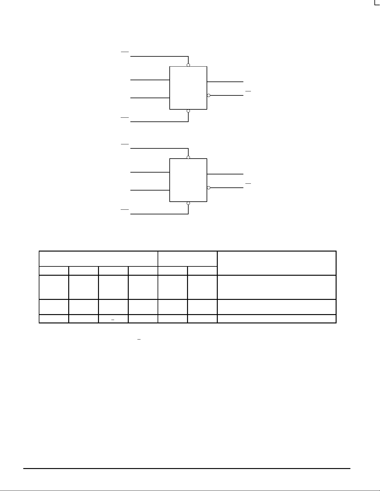
CD1 D1 CP1 SD1 O1 O1 GND
Figure 1. 14–Lead Pinout (Top View)
D2 CP2 SD2 O2 O2
1314 12 11 10 9 8
21 34567
14–LEAD TSSOP PACKAGE
14–LEAD SOIC EIAJ PACKAGE
PIN NAMES
Pins
CP1, CP2
D1, D2
CD1
, CD2
SD1, SD2
On, On
D SUFFIX
14–LEAD SOIC PACKAGE
CASE 751A–03
DT SUFFIX
CASE 948G–01
M SUFFIX
CASE 965–01
Function
Clock Pulse Inputs
Data Inputs
Direct Clear Inputs
Direct Set Inputs
Outputs
6/97
Motorola, Inc. 1997
1
REV 0
MC74LVX74
SD1
CP1 CP
CD1
SD2
CP2 CP
CD2
4
2
D1 D
3
1
10
12
D2 D
11
13
Figure 2. Logic Diagram
SD
CD
SD
CD
5
Q
Q
Q
Q
O1
6
O1
9
O2
8
O2
INPUTS OUTPUTS
SDn CDn CPn Dn On On
L
H
L L X X H H Undetermined
H
H
H H ↑ X NC NC Hold
H = High Voltage Level; h = High V oltage Level One Setup T ime Prior to the Low–to–High Clock Transition; L = Low Voltage Level; l = Low
Voltage Level One Setup T ime Prior to the Low–to–High Clock T ransition; NC = No Change; X = High or Low Voltage Level or Transitions
are Acceptable; ↑ = Low–to–High Transition; ↑
H
L
H
H
X
X
↑
↑
X
X
h
l
= Not a Low–to–High Transition; For ICC Reasons DO NOT FLOAT Inputs
H
L
H
L
L
H
L
H
OPERATING MODE
Asynchronous Set
Asynchronous Clear
Load and Read Register
MOTOROLA LCX DATA
2
BR1339 — REV 3
MC74LVX74
ОООООО
ОООООО
V
CC
Î
Î
ОООООО
Î
Î
Î
Î
Î
ОООООО
Î
Î
Î
Î
Î
Î
Î
ОООООО
Î
Î
Î
Î
Î
Î
Î
Î
Î
Î
Î
Î
Î
Î
Î
Î
ОООООО
Î
Î
Î
Î
Î
ОООООО
ОООООО
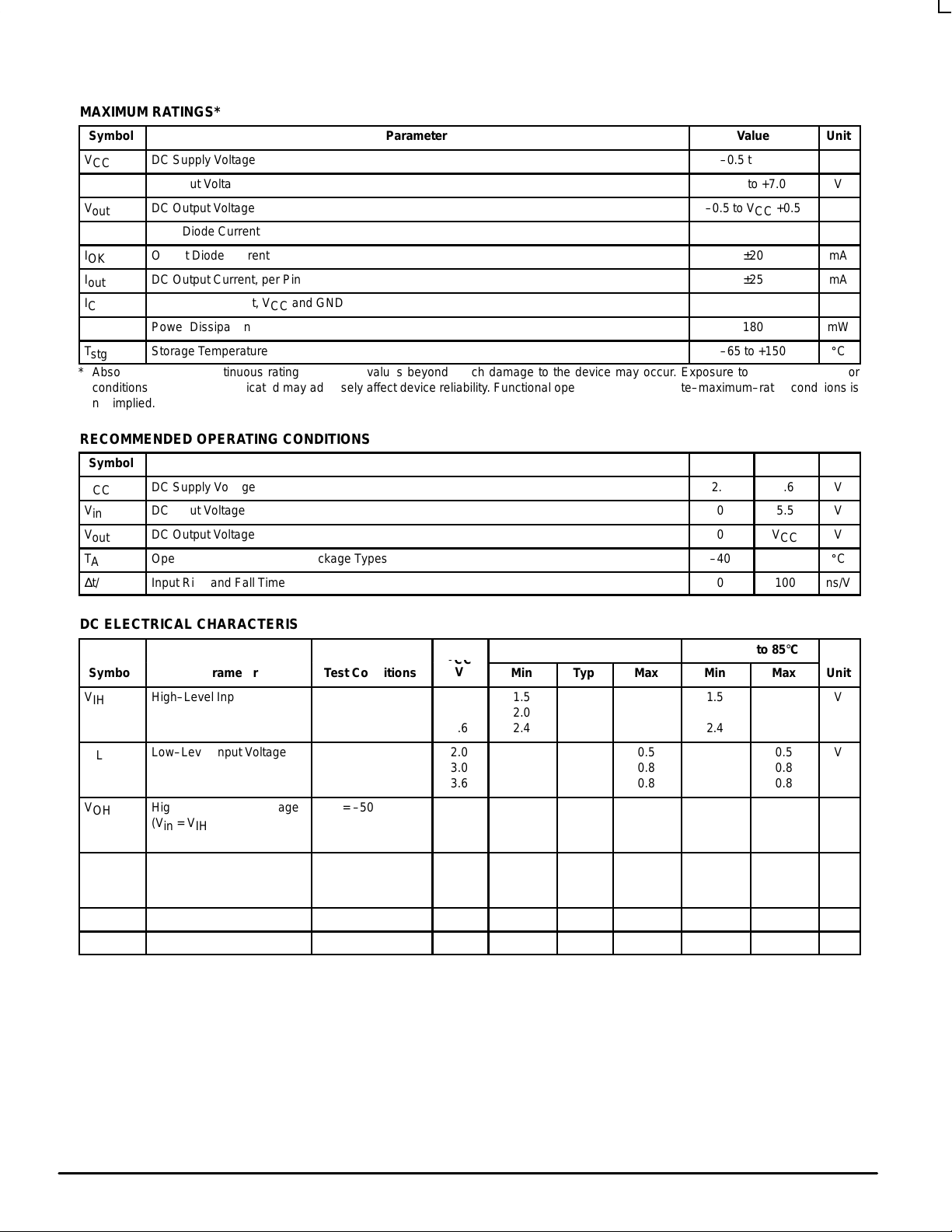
MAXIMUM RATINGS*
Symbol
V
V
V
I
I
I
I
P
T
CC
in
out
IK
OK
out
CC
D
stg
DC Supply Voltage
DC Input Voltage
DC Output Voltage
Input Diode Current
Output Diode Current
DC Output Current, per Pin
DC Supply Current, VCC and GND Pins
Power Dissipation
Storage Temperature
* Absolute maximum continuous ratings are those values beyond which damage to the device may occur. Exposure to these conditions or
conditions beyond those indicated may adversely affect device reliability. Functional operation under absolute–maximum–rated conditions is
not implied.
RECOMMENDED OPERATING CONDITIONS
Symbol
V
CC
V
in
V
out
T
A
∆t/∆V
DC Supply Voltage
DC Input Voltage
DC Output Voltage
Operating Temperature, All Package Types
Input Rise and Fall Time
Parameter
Parameter
Value
–0.5 to +7.0
–0.5 to +7.0
–0.5 to VCC +0.5
–20
±20
±25
±50
180
–65 to +150
Min
2.0
0
0
–40
0
Max
3.6
5.5
V
CC
+85
100
Unit
V
V
V
mA
mA
mA
mA
mW
_
C
Unit
V
V
V
_
C
ns/V
DC ELECTRICAL CHARACTERISTICS
Symbol
V
IH
ÎÎ
V
IL
ÎÎ
V
OH
ÎÎ
ÎÎ
V
OL
ÎÎ
I
in
I
CC
Parameter
High–Level Input Voltage
ОООООО
Low–Level Input Voltage
ОООООО
High–Level Output Voltage
ОООООО
(Vin = VIH or VIL)
ОООООО
Low–Level Output Voltage
(Vin = VIH or VIL)
ОООООО
Input Leakage Current
Quiescent Supply Current
ОООООÎÎ
ОООООÎÎ
IOH = –50µA
ООООО
IOH = –50µA
IOH = –4mA
ООООО
IOL = 50µA
IOL = 50µA
ООООО
IOL = 4mA
Vin = 5.5V or GND
Vin = VCC or GND
Test Conditions
V
V
2.0
3.0
3.6
2.0
3.0
3.6
2.0
Î
3.0
3.0
Î
2.0
3.0
Î
3.0
3.6
3.6
TA = 25°C
Min
Typ
Max
1.5
2.0
ÎÎ
2.4
ÎÎÎÎÎÎÎ
0.5
ÎÎÎÎÎÎÎ
1.9
ÎÎ
2.9
2.58
ÎÎ
2.0
Î
3.0
Î
0.0
0.0
ÎÎÎÎ
0.8
0.8
ÎÎ
ÎÎ
0.1
0.1
ÎÎ
0.36
±0.1
2.0
TA = – 40 to 85°C
Min
Max
1.5
2.0
2.4
ÎÎÎÎ
0.5
ÎÎÎÎÎ
0.8
0.8
1.9
ÎÎ
2.9
2.48
ÎÎ
ÎÎ
ÎÎ
0.1
0.1
ÎÎÎÎÎ
0.44
±1.0
20.0
Unit
V
V
Î
V
Î
Î
V
Î
µA
µA
LCX DATA
BR1339 — REV 3
3 MOTOROLA
 Loading...