


Motorola MC74LVX373M, MC74LVX373DT, MC74LVX373D Datasheet
SEMICONDUCTOR TECHNICAL DATA
1
REV 0
Motorola, Inc. 1997
6/97
"
!
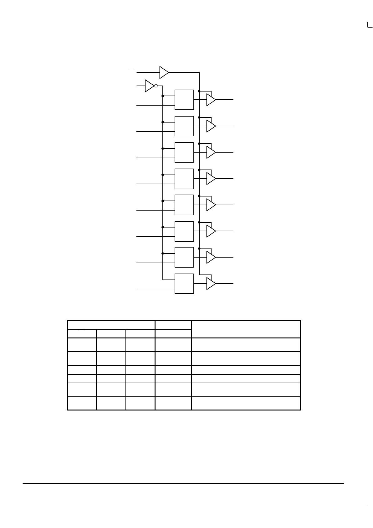
The MC74LVX373 is an advanced high speed CMOS octal latch with
3–state outputs. The inputs tolerate voltages up to 7V, allowing the
interface of 5V systems to 3V systems.
This 8–bit D–type latch is controlled by a latch enable input and an
output enable input. When the output enable input is high, the eight
outputs are in a high impedance state.
• High Speed: t
PD
= 5.8ns (Typ) at VCC = 3.3V
• Low Power Dissipation: I
CC
= 4µA (Max) at TA = 25°C
• Power Down Protection Provided on Inputs
• Balanced Propagation Delays
• Low Noise: V
OLP
= 0.8V (Max)
• Pin and Function Compatible with Other Standard Logic Families
• Latchup Performance Exceeds 300mA
• ESD Performance: HBM > 2000V; Machine Model > 200V
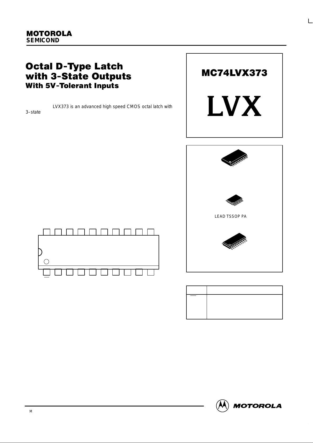
Figure 1. 20–Lead Pinout (Top View)
1920 18 17 16 15 14
21 34567
V
CC
13
8
12
9
11
10
O7 D7 D6 O6 O5 D5 D4 O4 LE
OE
O0 D0 D1 O1 O2 D2 D3 O3 GND
LVX
LOW–VOLTAGE CMOS
DW SUFFIX
20–LEAD SOIC PACKAGE
CASE 751D–04
DT SUFFIX
20–LEAD TSSOP PACKAGE
CASE 948E–02
M SUFFIX
20–LEAD SOIC EIAJ PACKAGE
CASE 967–01
PIN NAMES
Function
Output Enable Input
Latch Enable Input
Data Inputs
3–State Latch Outputs
Pins
OE
LE
D0–D7
O0–O7
MC74LVX373
MOTOROLA LCX DATA
BR1339 — REV 3
2
O0
D0
O1
D1
O2
D2
O3
D3
O4
D4
O5
D5
O6
D6
O7
D7
Figure 2. Logic Diagram
nLE
Q
D
nLE
Q
D
nLE
Q
D
nLE
Q
D
nLE
Q
D
nLE
Q
D
nLE
Q
D
nLE
Q
D
LE
OE
3
4
7
8
13
14
17
18
2
5
6
9
12
15
16
19
11
1
INPUTS OUTPUTS
OE LE Dn On OPERATING MODE
L
L
H
H
H
L
H
L
Transparent (Latch Disabled); Read Latch
L
L
L
L
h
l
H
L
Latched (Latch Enabled) Read Latch
L L X NC Hold; Read Latch
H L X Z Hold; Disabled Outputs
H
H
H
H
H
L
Z
Z
Transparent (Latch Disabled); Disabled Outputs
H
H
L
L
h
l
Z
Z
Latched (Latch Enabled); Disabled Outputs
H = High Voltage Level; h = High Voltage Level One Setup Time Prior to the Latch Enable High–to–Low
Transition; L = Low V oltage Level; l = Low Voltage Level One Setup Time Prior to the Latch Enable High–to–Low
Transition; NC = No Change, State Prior to the Latch Enable High–to–Low T ransition; X = High or Low V oltage
Level or Transitions are Acceptable; Z = High Impedance State; For ICC Reasons DO NOT FLOAT Inputs
MC74LVX373
LCX DATA
BR1339 — REV 3
3 MOTOROLA
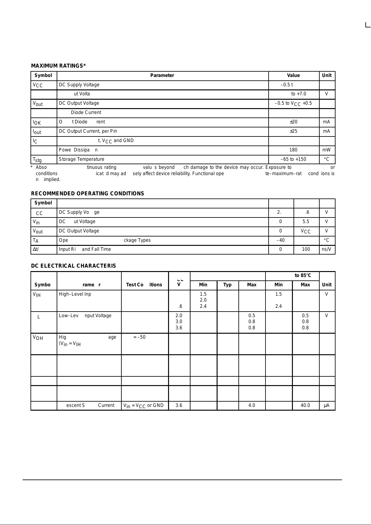
MAXIMUM RATINGS*
Symbol
Parameter
Value
Unit
V
CC
DC Supply Voltage
–0.5 to +7.0
V
V
in
DC Input Voltage
–0.5 to +7.0
V
V
out
DC Output Voltage
–0.5 to VCC +0.5
V
I
IK
Input Diode Current
–20
mA
I
OK
Output Diode Current
±20
mA
I
out
DC Output Current, per Pin
±25
mA
I
CC
DC Supply Current, VCC and GND Pins
±75
mA
P
D
Power Dissipation
180
mW
T
stg
Storage Temperature
–65 to +150
_
C
* Absolute maximum continuous ratings are those values beyond which damage to the device may occur. Exposure to these conditions or
conditions beyond those indicated may adversely affect device reliability. Functional operation under absolute–maximum–rated conditions is
not implied.
RECOMMENDED OPERATING CONDITIONS
Symbol
Parameter
Min
Max
Unit
V
CC
DC Supply Voltage
2.0
3.6
V
V
in
DC Input Voltage
0
5.5
V
V
out
DC Output Voltage
0
V
CC
V
T
A
Operating Temperature, All Package Types
–40
+85
_
C
∆t/∆V
Input Rise and Fall Time
0
100
ns/V
DC ELECTRICAL CHARACTERISTICS
ОООООО
V
TA = 25°C
TA = – 40 to 85°C
Symbol
Parameter
ОООООО
Test Conditions
V
CC
V
Min
Typ
Max
Min
Max
Unit
ÎÎ
Î
V
IH
ОООООО
Î
High–Level Input Voltage
ОООООО
ОООООÎÎ
Î
2.0
3.0
3.6
ÎÎ
Î
1.5
2.0
2.4
ÎÎÎÎÎÎÎ
Î
1.5
2.0
2.4
ÎÎÎÎ
V
ÎÎ
Î
V
IL
ОООООО
Î
Low–Level Input Voltage
ОООООО
ОООООÎÎ
Î
2.0
3.0
3.6
ÎÎÎÎÎÎÎ
Î
0.5
0.8
0.8
ÎÎÎÎÎ
Î
0.5
0.8
0.8
Î
V
ÎÎ
Î
ÎÎ
Î
V
OH
ОООООО
Î
ОООООО
Î
High–Level Output Voltage
(Vin = VIH or VIL)
ОООООО
ООООО
Î
ООООО
Î
IOH = –50µA
IOH = –50µA
IOH = –4mA
Î
Î
Î
Î
2.0
3.0
3.0
ÎÎ
Î
ÎÎ
Î
1.9
2.9
2.58
Î
Î
Î
Î
2.0
3.0
ÎÎ
Î
ÎÎ
Î
ÎÎ
Î
ÎÎ
Î
1.9
2.9
2.48
ÎÎ
Î
ÎÎ
Î
Î
Î
V
ÎÎ
Î
V
OL
ОООООО
Î
Low–Level Output Voltage
(Vin = VIH or VIL)
ОООООО
ООООО
Î
IOL = 50µA
IOL = 50µA
IOL = 4mA
Î
Î
2.0
3.0
3.0
ÎÎÎÎ
Î
0.0
0.0
ÎÎ
Î
0.1
0.1
0.36
ÎÎÎÎÎ
Î
0.1
0.1
0.44
Î
V
I
in
Input Leakage Current
ОООООО
Vin = 5.5V or GND
3.6
±0.1
±1.0
µA
ÎÎ
Î
I
OZ
ОООООО
Î
Maximum Three–State
Leakage Current
ОООООО
ООООО
Î
Vin = VIL or V
IH
V
out
= VCC or GND
Î
Î
3.6
ÎÎÎÎÎÎÎ
Î
±0.25
ÎÎÎÎÎ
Î
±2.5
Î
µA
I
CC
Quiescent Supply Current
ОООООО
Vin = VCC or GND
3.6
4.0
40.0
µA
 Loading...