

MOTOROLA MC10EP56DT, MC10EP56DTR2 Datasheet
MC10EP56
Product Preview
Dual Differential
2:1 Multiplexer
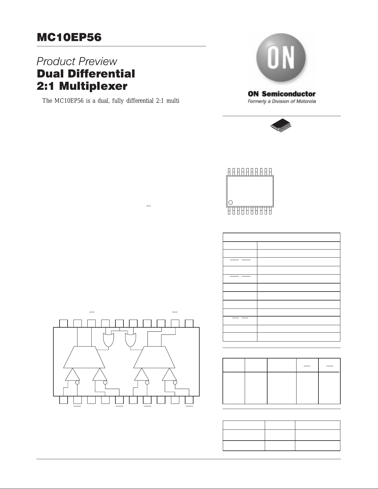
The MC10EP56 is a dual, fully differential 2:1 multiplexer. The
differential data path makes the device ideal for multiplexing low
skew clock or other skew sensitive signals. Multiple VBB pins are
provided to ease AC coupling of input signals. If used, the VBB output
should be bypassed to ground with a 0.01µF capacitor .
The device features both individual and common select inputs to
address both data path and random logic applications.
• 350ps Typical Propagation Delays
• Typical Frequency 3.0GHz
• 20–Lead TSSOP Package
• PECL mode: 3.0V to 5.5V V
• ECL mode: 0V V
with VEE = –3.0V to –5.5V
CC
• Separate and Common Select
• Internal Input Resistors: Pulldown on D, D
• Q Output will default LOW with inputs open or at V
• ESD Protection: >4KV HBM, >200V MM
• V
BB
Outputs
• New Differential Input Common Mode Range
• Moisture Sensitivity Level 1, Indefinite Time Out of Drypack.
For Additional Information, See Application Note AND8003/D
• Flammability Rating: UL–94 code V–0 @ 1/8”,
Oxygen Index 28 to 34
• Transistor Count = 140 devices
Q0
VCC Q0
1920
SEL0 SEL1 VCC Q1 Q1 V
1718 16 15 14 13 12
with VEE = 0V
CC
COM_SEL
EE
EE
11
http://onsemi.com
20
1
TSSOP–20
DT SUFFIX
CASE 948E
MARKING DIAGRAM*
MC10
EP56
ALYW
*For additional information, see Application Note
AND8002/D
A = Assembly Location
L = Wafer Lot
Y = Y ear
W = Work Week
PIN DESCRIPTION
PIN
D0a–D1a
D0a
–D1a ECL Input Data a Invert
D0b–D1b
–D1b ECL Input Data b Invert
D0b
SEL0–SEL1
COM_SEL ECL Common Select Input
V
, V
BB0
BB1
Q0–Q1 ECL True Outputs
Q0–Q1 ECL Inverted Outputs
V
CC
V
EE
FUNCTION
ECL Input Data a
ECL Input Data b
ECL Indiv. Select Input
Output Reference Voltage
Positive Supply
Negative, 0 Supply
10 1 0
21
D0a
56789
43
D0bD0b D1aVBBO
D1aD0a
10
VBB1 D1bD1b
Figure 1. 20–Lead TSSOP (Top View) and Logic Diagram
This document contains information on a product under development. ON Semiconductor
reserves the right to change or discontinue this product without notice.
Semiconductor Components Industries, LLC, 1999
January , 2000 – Rev. 2
1 Publication Order Number:
TRUTH TABLE
SEL0
X
L
L
H
H
SEL1
X
L
H
H
L
COM_SEL
H
L
L
L
L
Q0,
Q0
a
b
b
a
a
Q1,
Q1
a
b
a
a
b
ORDERING INFORMATION
Device Package Shipping
MC10EP56DT TSSOP 75 Units/Rail
MC10EP56DTR2 TSSOP 2500 Tape & Reel
MC10EP56/D
MC10EP56
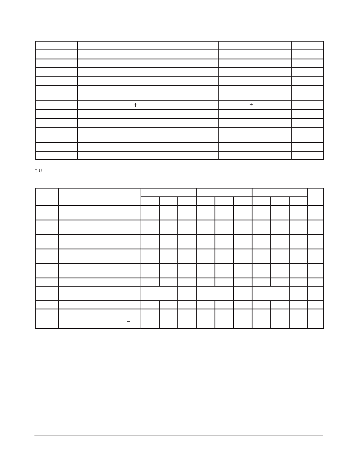
MAXIMUM RATINGS*
Symbol Parameter Value Unit
V
EE
V
CC
V
I
V
I
I
out
I
BB
T
A
T
stg
θ
JA
θ
JC
T
sol
* Maximum Ratings are those values beyond which damage to the device may occur.
{
Use for inputs of same package only.
DC CHARACTERISTICS, ECL/LVECL (VCC = 0V; VEE = –5.5V to –3.0V) (Note 4.)
Symbol Characteristic Min Typ Max Min Typ Max Min Typ Max Unit
IEE
V
OH
V
OL
V
IH
V
IL
V
BB
V
IHCMR
I
IH
I
IL
NOTE: 10EP circuits are designed to meet the DC specifications shown in the above table after thermal equilibrium has been established. The
1. VCC = 0V, VEE = V
2. All loading with 50 ohms to VCC–2.0 volts.
3. V
4. Input and output parameters vary 1:1 with VCC.
Power Supply Current
(Note 1.)
Output HIGH Voltage
(Note 2.)
Output LOW Voltage
(Note 2.)
Input HIGH Voltage
Single Ended
Input LOW Voltage
Single Ended
Output Voltage Reference –1510 –1410 –1310 –1445 –1345 –1245 –1385 –1285 –1185 mV
Input HIGH Voltage Common Mode
Range (Note 3.)
Input HIGH Current 150 150 150 µA
Input LOW Current
circuit is in a test socket or mounted on a printed circuit board and transverse airflow greater than 500lfpm is maintained.
min varies 1:1 with VEE, max varies 1:1 with VCC.
IHCMR
Power Supply (VCC = 0V) –6.0 to 0 VDC
Power Supply (VEE = 0V) 6.0 to 0 VDC
Input Voltage (VCC = 0V, VI not more negative than VEE) –6.0 to 0 VDC
Input Voltage (VEE = 0V, VI not more positive than VCC) 6.0 to 0 VDC
Output Current Continuous
VBB Sink/Source Current
Operating Temperature Range –40 to +85 °C
Storage Temperature –65 to +150 °C
Thermal Resistance (Junction–to–Ambient) Still Air
Thermal Resistance (Junction–to–Case) 23 to 41 ± 5% °C/W
Solder Temperature (<2 to 3 Seconds: 245°C desired) 265 °C
SEL, COM_SEL, D
to V
EEmin
EEmax
{
–40°C 25°C 85°C
50 65 88 50 65 88 50 65 88 mA
–1135 –1060 –885 –1070 –945 –820 –1010 –885 –760 mV
–1935 –1810 –1685 –1870 –1745 –1620 –1810 –1685 –1560 mV
–1210 –885 –1145 –820 –1085 –760 mV
–1935 –1610 –1870 –1545 –1810 –1485 mV
VEE+2.0 0.0 VEE+2.0 0.0 VEE+2.0 0.0 V
0.5
D
, all other pins floating.
–150
Surge
500lfpm
0.5
–150
50
100
± 0.5 mA
140
100
0.5
–150
mA
°C/W
µA
http://onsemi.com
2
MC10EP56
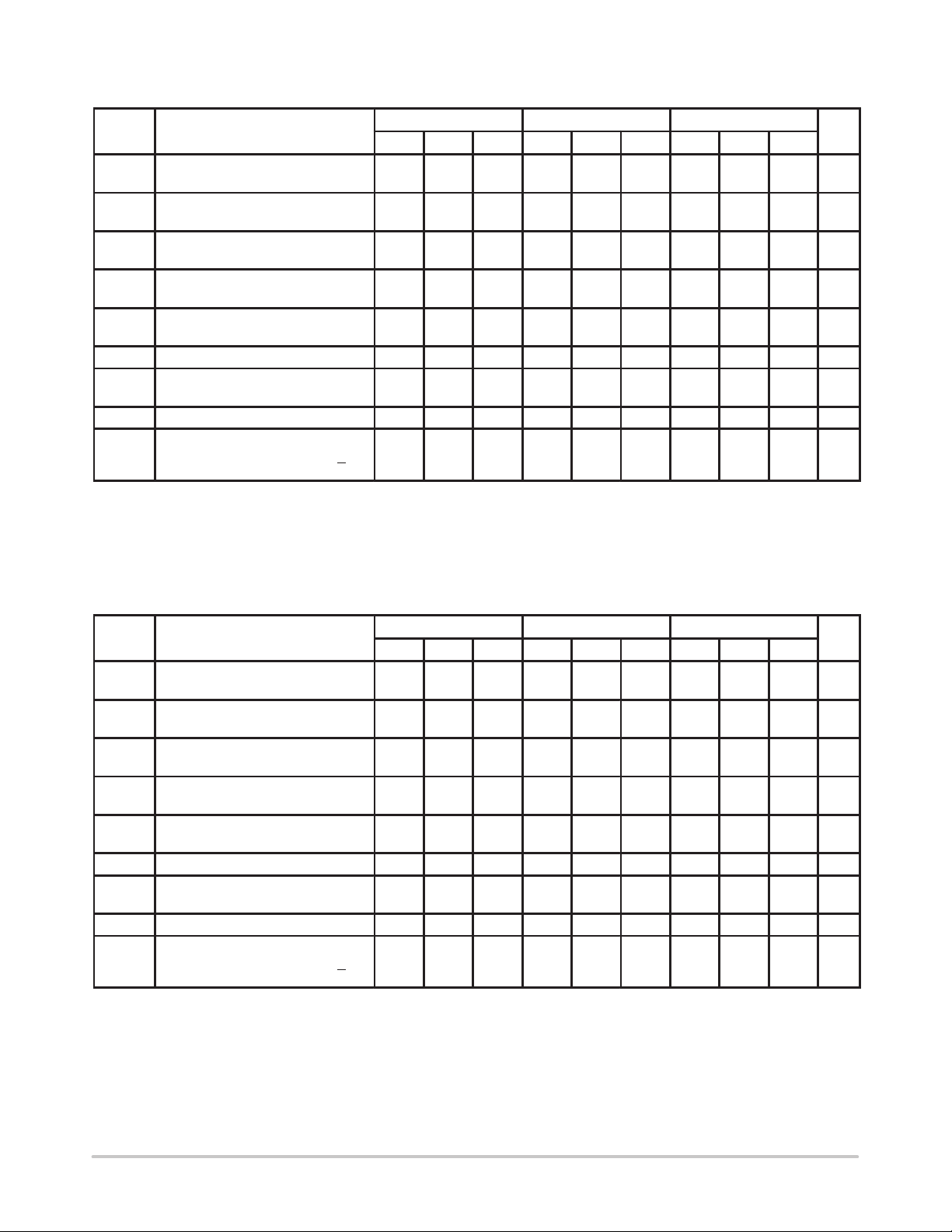
DC CHARACTERISTICS, LVPECL (VCC = 3.3V ± 0.3V, VEE = 0V) (Note 8.)
–40°C 25°C 85°C
Symbol Characteristic Min Typ Max Min Typ Max Min Typ Max Unit
IEE
V
OH
V
OL
V
IH
V
IL
V
BB
V
IHCMR
I
IH
I
IL
NOTE: 10EP circuits are designed to meet the DC specifications shown in the above table after thermal equilibrium has been established. The
5. VCC = 3.3V, VEE = 0V, all other pins floating.
6. All loading with 50 ohms to VCC–2.0 volts.
7. V
8. Input and output parameters vary 1:1 with VCC.
Power Supply Current
(Note 5.)
Output HIGH Voltage
(Note 6.)
Output LOW Voltage
(Note 6.)
Input HIGH Voltage
Single Ended
Input LOW Voltage
Single Ended
Output Voltage Reference 1790 1890 1990 1855 1955 2055 1915 2015 2115 mV
Input HIGH Voltage Common Mode
Range (Note 7.)
Input HIGH Current 150 150 150 µA
Input LOW Current
circuit is in a test socket or mounted on a printed circuit board and transverse airflow greater than 500lfpm is maintained.
min varies 1:1 with VEE, max varies 1:1 with VCC.
IHCMR
SEL, COM_SEL, D
D
50 65 88 50 65 88 50 65 88 mA
2165 2240 2415 2230 2355 2480 2290 2415 2540 mV
1365 1490 1615 1430 1555 1680 1490 1615 1740 mV
2090 2415 2155 2480 2215 2540 mV
1365 1690 1430 1755 1490 1815 mV
2.0 3.3 2.0 3.3 2.0 3.3 V
0.5
–150
0.5
–150
0.5
–150
µA
DC CHARACTERISTICS, PECL (VCC = 5.0V ± 0.5V, VEE = 0V) (Note 12.)
–40°C 25°C 85°C
Symbol Characteristic Min Typ Max Min Typ Max Min Typ Max Unit
IEE
V
OH
V
OL
V
IH
V
IL
V
BB
V
IHCMR
I
IH
I
IL
NOTE: 10EP circuits are designed to meet the DC specifications shown in the above table after thermal equilibrium has been established. The
9. VCC = 5.0V, VEE = 0V, all other pins floating.
10.All loading with 50 ohms to VCC–2.0 volts.
11. V
12.Input and output parameters vary 1:1 with VCC.
Power Supply Current
(Note 9.)
Output HIGH Voltage
(Note 10.)
Output LOW Voltage
(Note 10.)
Input HIGH Voltage
Single Ended
Input LOW Voltage
Single Ended
Output Voltage Reference 3490 3590 3690 3555 3655 3755 3615 3715 3815 mV
Input HIGH Voltage Common Mode
Range (Note 11.)
Input HIGH Current 150 150 150 µA
Input LOW Current
circuit is in a test socket or mounted on a printed circuit board and transverse airflow greater than 500lfpm is maintained.
min varies 1:1 with VEE, max varies 1:1 with VCC.
IHCMR
SEL, COM_SEL, D
D
50 65 88 50 65 88 50 65 88 mA
3865 3940 4115 3930 4055 4180 3990 4115 4240 mV
3065 3190 3315 3130 3255 3380 3190 3315 3440 mV
3790 4115 3855 4180 3915 4240 mV
3065 3390 3130 3455 3190 3515 mV
2.0 5.0 2.0 5.0 2.0 5.0 V
0.5
–150
0.5
–150
0.5
–150
µA
http://onsemi.com
3
 Loading...