

MOTOROLA MC10EP35D, MC10EP35DR2 Datasheet
MC10EP35
JK Flip Flop
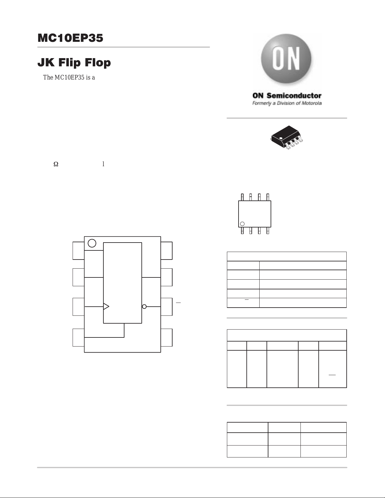
The MC10EP35 is a higher speed/low voltage version of the EL35
JK flip flop. The J/K data enters the master portion of the flip flop
when the clock is LOW and is transferred to the slave, and thus the
outputs, upon a positive transition of the clock. The reset pin is
asynchronous and is activated with a logic HIGH.
• 300ps Propagation Delay
• High Bandwidth to 3 GHz T ypical
• High Bandwidth Output Transistors
• PECL mode: 3.0V to 5.5V V
• ECL mode: 0V V
• 75k
W
Internal Input Pulldown Resistors
with VEE = –3.0V to –5.5V
CC
• Q Output will default LOW with inputs open or at V
• ESD Protection: >4KV HBM, >200V MM
• Moisture Sensitivity Level 1, Indefinite Time Out of Drypack.
For Additional Information, See Application Note AND8003/D
• Flammability Rating: UL–94 code V–0 @ 1/8”,
Oxygen Index 28 to 34
• Transistor Count = 77 devices
J
1
2
K
3
CC
J
K
Flip Flop
with VEE = 0V
78Q
6
EE
V
QCLK
CC
http://onsemi.com
8
1
SO–8
D SUFFIX
CASE 751
MARKING DIAGRAM
8
HEP35
ALYW
1
*For additional information, see Application Note
AND8002/D
PIN DESCRIPTION
PIN
CLK
J, K ECL Signal Inputs
RESET ECL Asynchronous Reset
Q, Q ECL Data Outputs
A = Assembly Location
L = Wafer Lot
Y = Year
W = Work Week
FUNCTION
ECL Clock Inputs
R
RESET
Figure 1. 8–Lead Pinout (Top View) and Logic Diagram
Semiconductor Components Industries, LLC, 1999
September, 1999 – Rev. 1.0
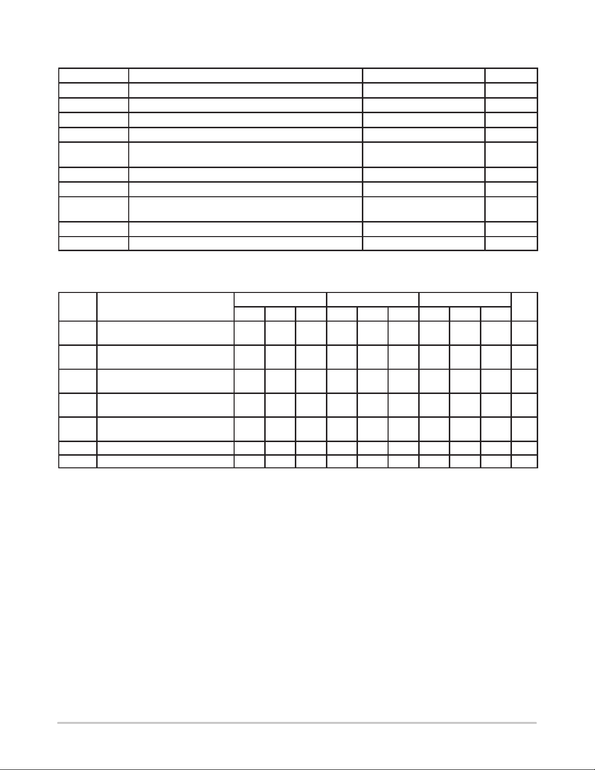
45
V
EE
J
L
L
H
H
X
Z = LOW to HIGH Transition
Device Package Shipping
MC10EP35D SOIC 98 Units/Rail
MC10EP35DR2 SOIC 2500 Tape & Reel
1 Publication Order Number:
TRUTH TABLE
RESET
K
L
H
L
H
X
ORDERING INFORMATION
L
L
L
L
H
CLK
Z
Z
Z
Z
X
Qn+1
Qn
L
H
Qn
L
MC10EP35/D
MC10EP35
MAXIMUM RATINGS*
Symbol Parameter Value Unit
V
EE
V
CC
V
I
V
I
I
out
T
A
T
stg
θ
JA
θ
JC
T
sol
* Maximum Ratings are those values beyond which damage to the device may occur.
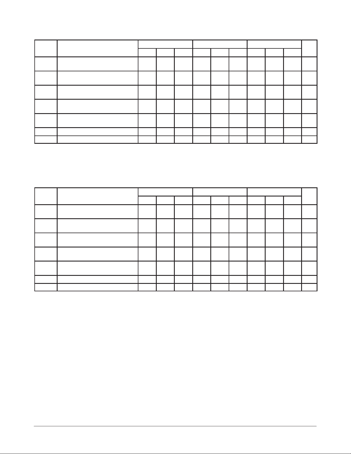
DC CHARACTERISTICS, ECL/LVECL (VCC = 0V; VEE = –5.5V to –3.0V) (Note 3.)
Symbol Characteristic Min Typ Max Min Typ Max Min Typ Max Unit
IEE
V
OH
V
OL
V
IH
V
IL
I
IH
I
IL
NOTE: 10EP circuits are designed to meet the DC specifications shown in the above table after thermal equilibrium has been established. The
1. VCC = 0V, VEE = V
2. All loading with 50 ohms to VCC–2.0 volts.
3. Input and output parameters vary 1:1 with VCC.
Power Supply Current
(Note 1.)
Output HIGH Voltage
(Note 2.)
Output LOW Voltage
(Note 2.)
Input HIGH Voltage
Single Ended
Input LOW Voltage
Single Ended
Input HIGH Current 150 150 150 µA
Input LOW Current 0.5 0.5 0.5 µA
circuit is in a test socket or mounted on a printed circuit board and transverse airflow greater than 500lfpm is maintained.
Power Supply (VCC = 0V) –6.0 to 0 VDC
Power Supply (VEE = 0V) 6.0 to 0 VDC
Input Voltage (VCC = 0V, VI not more negative than VEE) –6.0 to 0 VDC
Input Voltage (VEE = 0V, VI not more positive than VCC) 6.0 to 0 VDC
Output Current Continuous
Operating Temperature Range –40 to +85 °C
Storage Temperature –65 to +150 °C
Thermal Resistance (Junction–to–Ambient) Still Air
Thermal Resistance (Junction–to–Case) 41 to 44 ± 5% °C/W
Solder Temperature (<2 to 3 Seconds: 245°C desired) 265 °C
–40°C 25°C 85°C
30 40 50 30 40 50 30 40 50 mA
–1135 –1060 –885 –1070 –945 –820 –1010 –885 –760 mV
–1935 –1810 –1685 –1870 –1745 –1620 –1810 –1685 –1560 mV
–1210 –885 –1145 –820 –1085 –760 mV
–1935 –1610 –1870 –1545 –1810 –1485 mV
EEmin
to V
, all other pins floating.
EEmax
Surge
500lfpm
50
100
190
130
mA
°C/W
http://onsemi.com
2
MC10EP35
DC CHARACTERISTICS, LVPECL (VCC = 3.3V ± 0.3V, VEE = 0V) (Note 6.)
–40°C 25°C 85°C
Symbol Characteristic Min Typ Max Min Typ Max Min Typ Max Unit
IEE
V
OH
V
OL
V
IH
V
IL
I
IH
I
IL
NOTE: 10EP circuits are designed to meet the DC specifications shown in the above table after thermal equilibrium has been established. The
4. VCC = 3.3V, VEE = 0V, all other pins floating.
5. All loading with 50 ohms to VCC–2.0 volts.
6. Input and output parameters vary 1:1 with VCC.
Power Supply Current
(Note 4.)
Output HIGH Voltage
(Note 5.)
Output LOW Voltage
(Note 5.)
Input HIGH Voltage
Single Ended
Input LOW Voltage
Single Ended
Input HIGH Current 150 150 150 µA
Input LOW Current 0.5 0.5 0.5 µA
circuit is in a test socket or mounted on a printed circuit board and transverse airflow greater than 500lfpm is maintained.
DC CHARACTERISTICS, PECL (VCC = 5.0V ± 0.5V, VEE = 0V) (Note 9.)
Symbol Characteristic Min Typ Max Min Typ Max Min Typ Max Unit
IEE
V
OH
V
OL
V
IH
V
IL
I
IH
I
IL
NOTE: 10EP circuits are designed to meet the DC specifications shown in the above table after thermal equilibrium has been established. The
7. VCC = 5.0V, VEE = 0V, all other pins floating.
8. All loading with 50 ohms to VCC–2.0 volts.
9. Input and output parameters vary 1:1 with VCC.
Power Supply Current
(Note 7.)
Output HIGH Voltage
(Note 8.)
Output LOW Voltage
(Note 8.)
Input HIGH Voltage
Single Ended
Input LOW Voltage
Single Ended
Input HIGH Current 150 150 150 µA
Input LOW Current 0.5 0.5 0.5 µA
circuit is in a test socket or mounted on a printed circuit board and transverse airflow greater than 500lfpm is maintained.
30 40 50 30 40 50 30 40 50 mA
2165 2240 2415 2230 2355 2480 2290 2415 2540 mV
1365 1490 1615 1430 1555 1680 1490 1615 1740 mV
2090 2415 2155 2480 2215 2540 mV
1365 1690 1430 1755 1490 1815 mV
–40°C 25°C 85°C
30 40 50 30 40 50 30 40 50 mA
3865 3940 4115 3930 4055 4180 3990 4115 4240 mV
3065 3190 3315 3130 3255 3380 3190 3315 3440 mV
3790 4115 3855 4180 3915 4240 mV
3065 3390 3130 3455 3190 3515 mV
http://onsemi.com
3
 Loading...