


PS21965-T
MITSUBISHI SEMICONDUCTOR <Dual-In-Line Package Intelligent Power Module>
PS21965-T/-AT/-CT/-TW
TRANSFER-MOLD TYPE
INSULATED TYPE
PS21965-T
INTEGRATED POWER FUNCTIONS
600V/20A low-loss CSTBTTM inverter bridge for three
phase DC-to-AC power conversion
INTEGRATED DRIVE, PROTECTION AND SYSTEM CONTROL FUNCTIONS
• For upper-leg IGBTS : Drive circuit, High voltage high-speed level shifting, Control supply under-voltage (UV) protection.
• For lower-leg IGBTS :
Drive circuit, Control supply under-voltage protection (UV), Short circuit protection (SC), Over temperature protection (OT).
• Fault signaling : Corresponding to an SC fault (Lower-leg IGBT), a UV fault (Lower-side supply) or an OT fault (LVIC temperature).
• Input interface : 3V, 5V line (High Active).
•UL Approved : Yellow Card No. E80276
APPLICATION
AC100V~200V three-phase inverter drive for small power motor control.
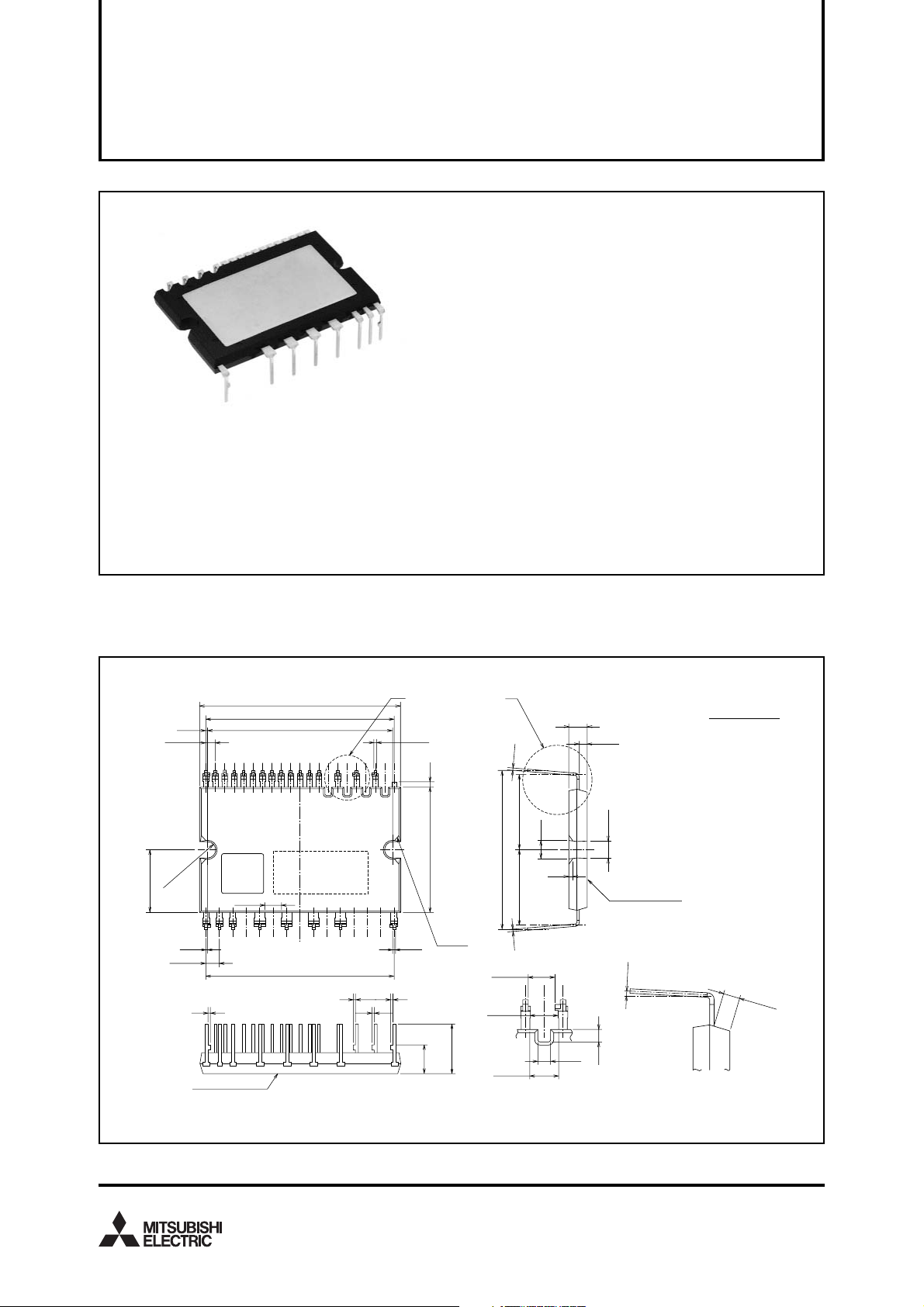
Fig. 1 PACKAGE OUTLINES (PS21965-T)
±0.5
38
20×1.778(=35.56)
0.28
±0.2
1.778
17 1
QR
2-R1.6
12
2.54
18
0.28
±0.2
0.5
HEAT SINK SIDE
Code
3 MIN
±0.3
35
Type name
Lot No.
14×2.54(=35.56)
A
16-0.5
(1)
±0.5
24
25
4-C1.2
8-0.6
0.50.5
0.5
±0.5
±0.5
9.5
5.5
B
3.5
±0.05
0.4
±0.5
14.4
(3.5)
±0.5
29.2
±0.5
14.4
0.4
2.5 MIN
(2.656)
(2.756)
DETAIL A DETAIL B
1.5
(3.3)
0.8
HEAT SINK SIDE
(0~5°)
(1.2)
(1.2)
Dimensions in mm
TERMINAL CODE
1. NC
2. V
UFB
3. V
VFB
4. V
WFB
5. U
P
6. V
P
7. W
P
8. V
P1
9. VNC *
10. U
N
11. V
N
12. W
N
13. V
N1
14. F
O
15. CIN
16. V
NC
*
17. NC
18. NC
19. NC
20. N
21. W
22. V
23. U
24. P
25. NC
1.5 MIN
*) Two VNC terminals (9 & 16 pin) are connected inside DIPIPM, please connect either one to the 15V power supply GND outside and
leave another one open.
Mar. 2009
MITSUBISHI SEMICONDUCTOR <Dual-In-Line Package Intelligent Power Module>
PS21965-T/-AT/-CT/-TW
TRANSFER-MOLD TYPE
INSULATED TYPE
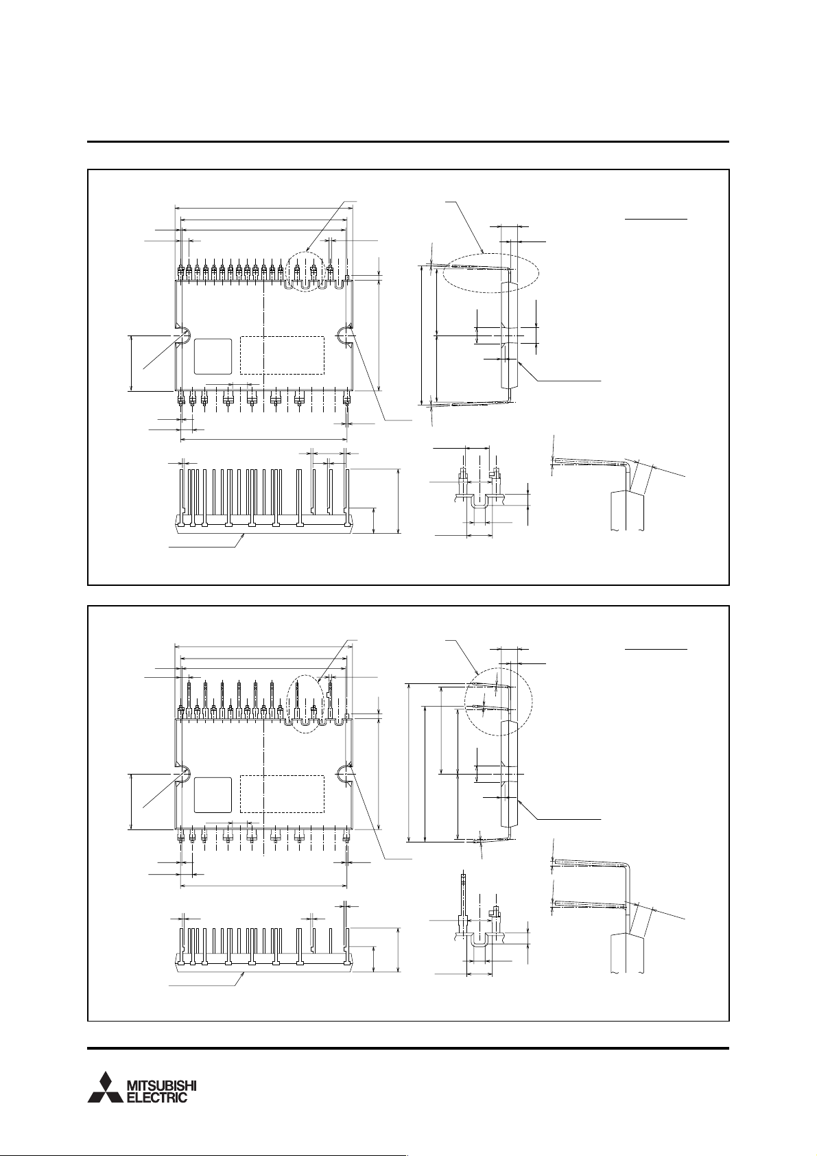
Fig. 2 LONG TERMINAL TYPE PACKAGE OUTLINES (PS21965-AT)
±0.5
38
20×1.778(=35.56)
1.778
0.28
±0.2
±0.3
35
A
16-0.5
B
3.5
±0.05
1.5
TERMINAL CODE
0.4
17 1
QR
2-R1.6
12
Code
Type name
Lot No.
3 MIN
18
0.28
±0.2
2.54
14×2.54(=35.56)
0.5
0.5
(1)
±0.5
14.4
±0.5
±0.5
24
29.4
(3.5)
±0.5
0.8
14.4
25
4-C1.2
8-0.6
0.50.5
0.4
2.5 MIN
(3.3)
HEAT SINK SIDE
(0~5°)
(2.656)
±0.5
14
±0.5
5.5
(2.756)
HEAT SINK SIDE
NC terminals (9 & 16 pin) are connected inside DIPIPM, please connect either one to the 15V power supply GND outside and
*) Two V
(1.2)
(1.2)
DETAIL A DETAIL B
leave another one open.
Dimensions in mm
1. NC
2. V
UFB
3. V
VFB
4. V
WFB
5. U
P
6. V
P
7. W
P
8. V
P1
9. VNC *
10. U
N
11. V
N
12. W
N
13. V
N1
14. F
O
15. CIN
16. V
NC
*
17. NC
18. NC
19. NC
20. N
21. W
22. V
23. U
24. P
25. NC
1.5 MIN
Fig. 3 ZIGZAG TERMINAL TYPE PACKAGE OUTLINES (PS21965-CT)
33.7
±0.5
29.2
±0.5
18.9
(2.656)
(2.756)
B
±0.5
14.4
±0.5
14.4
DETAIL A
±0.5
38
20×1.778(=35.56)
1.778
0.28
±0.2
±0.3
35
17 1
QR
2-R1.6
12
Code
Type name
Lot No.
3 MIN
18
0.28
±0.2
2.54
14×2.54(=35.56)
0.5
HEAT SINK SIDE
A
16-0.5
(1)
±0.5
±0.5
24
25
4-C1.2
8-0.6
0.5
0.5
±0.5
±0.5
9.5
5.5
(3.5)
3.5
±0.05
1.5
0.4
0.4
0.8
HEAT SINK SIDE
0.4
(0~5°)
(0~5°)
(1.2)
(1.2)
Dimensions in mm
TERMINAL CODE
1. NC
2. V
UFB
3. V
VFB
4. V
WFB
5. U
P
6. V
P
7. W
8. V
P1
9. VNC *
10. U
N
11. V
N
12. W
13. V
N1
14. F
O
15. CIN
16. V
NC
17. NC
18. NC
19. NC
20. N
21. W
22. V
23. U
24. P
25. NC
DETAIL B
P
N
*
1.5 MIN
*) Two VNC terminals (9 & 16 pin) are connected inside DIPIPM, please connect either one to the 15V power supply GND outside and
leave another one open.
Mar. 2009
2
MITSUBISHI SEMICONDUCTOR <Dual-In-Line Package Intelligent Power Module>
PS21965-T/-AT/-CT/-TW
TRANSFER-MOLD TYPE
INSULATED TYPE
Fig. 4 BOTH SIDES ZIGZAG TERMINAL TYPE PACKAGE OUTLINES (PS21965-TW)
±0.6
35.2
B
3.5
±0.05
1.5
0.4
±0.5
14.4
±0.5
14.4
(3.5)
0.4
0.8
0.4
0.4
HEAT SINK SIDE
°)
(0~5
°)
(0~5
±0.5
17.4
±0.5
29.2
±0.5
17.4
2.5 MIN
(2.656)
(1.2)
(2.756)
(1.2)
DETAIL A DETAIL B
±0.5
38
20×1.778(=35.56)
1.778
0.28
±0.25
±0.3
35
17 1
QR
2-R1.6
12
Code
Type name
Lot No.
3 MIN
18
(1.8)
0.28
±0.25
2.54
14×2.54(=35.56)
0.5
HEAT SINK SIDE
A
16-0.5
(1)
±0.5
24
25
4-C1.2
7-0.6
0.5
0.5
±0.5
11
±0.5
5.5
TERMINAL CODE
1. NC
2. V
3. V
4. V
5. U
6. V
7. W
8. V
9. VNC *
10. U
11. V
12. W
13. V
14. F
15. CIN
16. V
17. NC
18. NC
19. NC
20. N
21. W
22. V
23. U
24. P
25. NC
Dimensions in mm
UFB
VFB
WFB
P
P
P
P1
N
N
N
N1
O
NC
*
1.5 MIN
*) Two VNC terminals (9 & 16 pin) are connected inside DIPIPM, please connect either one to the 15V power supply GND outside and
leave another one open.
QR Code is registered trademark of DENSO WAVE INCORPORATED in Japan and other countries.
Fig. 5 INTERNAL FUNCTIONS BLOCK DIAGRAM (TYPICAL APPLICATION EXAMPLE)
CBU–
CBV–
CBW–
CBU+
CBV+
V
S
NC
CBW+
C2
C1
(Note 6)
S
U
V
W
(15V line)
(Note 7)
C1 : Electrolytic type with good temperature and frequency
characteristics
(Note : The capacitance value depends on the PWM control
scheme used in the applied system).
C2 : 0.22~2µF R-category ceramic capacitor for noise filtering.
Inrush current
limiter circuit
High-side input (PWM)
(3V, 5V line)(Note 1,
Input signal
conditioning
Level shifter
Protection
circuit (UV)
Drive circuit
P
2)
Input signal
conditioning
Level shifter
Drive circuit
Input signal
conditioning
Level shifter
Drive circuit
H-side IGBT
AC line input
(Note 4)
C
Z
Z : Surge absorber
C : AC filter (Ceramic capacitor 2.2~6.5nF)
(Note : Additionally, an appropriate line-to line
surge absorber circuit may become necessary
depending on the application environment).
Note1: Input logic is high-active. There is a 3.3kΩ (min) pull-down resistor built-in each input circuit. When using an external CR filter, please make it satisfy the
input threshold voltage.
2: By virtue of integrating an application specific type HVIC inside the module, direct coupling to MCU terminals without any opto-coupler or transformer
isolation is possible. (see also Fig. 11)
3: This output is open drain type. The signal line should be pulled up to the positive side of the 5V power supply with approximately 10kΩ resistor.
(see also Fig. 11)
4: The wiring between the power DC link capacitor and the P, N1 terminals should be as short as possible to protect the DIPIPM against catastrophic high
surge voltages. For extra precaution, a small film type snubber capacitor (0.1~0.22µF, high voltage type) is recommended to be mounted close to
these P & N1 DC power input pins.
5: High voltage (600V or more) and fast recovery type (less than 100ns) diodes should be used in the bootstrap circuit.
6: It is recommended to insert a Zener diode (24V/1W) between each pair of control supply terminals to prevent surge destruction.
7: Bootstrap negative electrodes should be connected to U, V, W terminals directly and separated from the main output wires.
N1
N
V
NC
CIN
Input signal conditioning
Low-side input (PWM)
(3V, 5V line)(Note 1, 2)
Drive circuit
Fo logic
F
O
Fault output (5V line)
(Note 3)
Protection
circuit
Control supply
Under-Voltage
protection
L-side IGBT
(Note 5)
DIPIPM
AC line output
(Note 6)
V
D
M
Mar. 2009
3
 Loading...